Language selection

Search

Patent 2350664 Summary

Third-party information liability

Some of the information on this Web page has been provided by external sources. The Government of Canada is not responsible for the accuracy, reliability or currency of the information supplied by external sources. Users wishing to rely upon this information should consult directly with the source of the information. Content provided by external sources is not subject to official languages, privacy and accessibility requirements.

Claims and Abstract availability

Any discrepancies in the text and image of the Claims and Abstract are due to differing posting times. Text of the Claims and Abstract are posted:

  • At the time the application is open to public inspection;
  • At the time of issue of the patent (grant).
(12) Patent Application: (11) CA 2350664
(54) English Title: LOGIC INPUT CIRCUIT WITH ENERGY TRANSFER AND ADAPTABLE IN INPUT VOLTAGE
(54) French Title: CIRCUIT LOGIQUE D'ENTREE A TRANSFERT D'ENERGIE ET ADAPTABLE EN FONCTION DE LA TENSION D'ENTREE
Status: Deemed Abandoned and Beyond the Period of Reinstatement - Pending Response to Notice of Disregarded Communication
Bibliographic Data
(51) International Patent Classification (IPC):
  • G05B 19/042 (2006.01)
  • G01R 19/155 (2006.01)
  • G01R 19/165 (2006.01)
  • G05B 19/418 (2006.01)
(72) Inventors :
  • PIRON, PATRICK (France)
  • DREVON, RICHARD (France)
  • FRANCOIS, OLIVIER (France)
(73) Owners :
  • SOPRANO
(71) Applicants :
  • SOPRANO (France)
(74) Agent: ROBIC AGENCE PI S.E.C./ROBIC IP AGENCY LP
(74) Associate agent:
(45) Issued:
(86) PCT Filing Date: 2000-09-08
(87) Open to Public Inspection: 2001-03-22
Availability of licence: N/A
Dedicated to the Public: N/A
(25) Language of filing: English

Patent Cooperation Treaty (PCT): Yes
(86) PCT Filing Number: PCT/FR2000/002484
(87) International Publication Number: WO 2001020414
(85) National Entry: 2001-05-09

(30) Application Priority Data:
Application No. Country/Territory Date
99/11491 (France) 1999-09-10

Abstracts

English Abstract


The invention concerns a logic input circuit for an industrial equipment
automatic system powered by a direct current voltage source, in particular a
battery (16), comprising a voltage amplifying energy converter (12) consisting
of an inductance coil L and a switching transistor TR, connected to the input
E1 of the circuit (10); a logic level sensor DL with optocoupler (20), and a
clock circuit H controlling the transistor switching TR by adjusting the
frequency or the cyclic ratio to be adapted in voltage to the signals applied
at the input E1, and the overvoltage value generated in logic high (1) by the
inductance coil L when the transistor TR is switched off-state.


French Abstract

Un circuit d'entrée logique pour un automatisme d'un équipement industriel alimenté par une source de tension continue, notamment une batterie (16), comporte: un convertisseur d'énergie (12) élévateur de tension composé d'une bobine d'inductance L et d'un transistor TR de commutation, connectés à l'entrée E1 du circuit (10); un détecteur de niveau logique DL à optocoupleur (20), et un circuit d'horloge H pilotant la commutation du transistor TR par réglage de la fréquence ou du rapport cyclique pour s'adapter en tension aux signaux appliqués à l'entrée E1, ainsi que la valeur de la surtension engendrée dans l'état logique haut (1) par la bobine d'inductance L lors de la commutation du transistor TR vers l'état bloqué.

Claims

Note: Claims are shown in the official language in which they were submitted.

6
Claims
1. A logic input circuit for an industrial equipment automatic control system
supplied by a DC voltage source, in particular a battery, said input circuit
comprising means for detection designed to deliver a measurement signal
representative of logic low state and of logic high state, comprising:
- a voltage step-up energy converter composed of an inductance coil and a
switching transistor, connected to the input of the circuit,
- a logic level detector connected either between the inductance coil and a
rectifier
diode of an energy recovery circuit or between a charging resistor and the
positive pole of the DC voltage source,
- and a clock circuit controlling switching of the transistor by adjustment of
the
frequency and duty cycle to perform voltage matching with the signals applied
to
the input, and also the value of the voltage surge generated in logic high
state by
the inductance coil when switching of the transistor to the off state takes
place.
2. The logic input circuit according to claim 1, wherein the switching
transistor is
connected between the input potential reference and a mid-point of connection
of
the inductance coil to the logic level detector or to the rectifier diode.
3. The logic input circuit according to claim 1, wherein the logic level
detector
comprises an optocoupler having an emitting diode connected between the
inductance coil and the rectifier diode, and a receiver delivering said
measurement
signal to an acquisition circuit.
4. The logic input circuit according to claim 1, wherein the logic level
detector
comprises an optocoupler having an emitting diode connected between the
charging resistor and the positive pole of the voltage source, and a receiver
delivering said measurement signal to an acquisition circuit.

7
5. The logic input circuit according to claim 1, wherein the resistor of the
energy
recovery circuit is electrically connected in series between the rectifier
diode and
the battery or the emitting diode.
6. The logic input circuit according to claim 5, wherein a first filtering
capacitor is
connected in parallel between the input potential reference and the mid-point
of
connection of the rectifier diode to the resistor.
7. The logic input circuit according to claim 6, wherein a second filtering
capacitor is
connected in parallel between the input potential reference and the input.

Description

Note: Descriptions are shown in the official language in which they were submitted.


CA 02350664 2001-05-09
LOGIC INPUT CIRCUIT WITH ENERGY TRANSFER AND ADAPTABLE IN INPUT VOLTAGE
Background of the Invention
The invention relates to a logic input arcuit for an irxiustrial equipment
automatic
control system supplied by a DC voltage source, in particular a battery, said
Input drcuit comprising means for detection designed to deliver a measurement
signal representative of the logic state when opening and closing of an input
contact take place, with a very low heat dissipation.
State of the art
A logic input board in electronic equipment for automatic control systems of
in-board installations, in particular of rail transport vehicles, generally
requires a large input current of about 10mA. The problem arising in
conventional equipment is then that of heat dissipation in the measuring
resistors, as a logic input in a voltage of 110 Volts for example, and a
current with an intensity of 10 mA, will dissipate a thermal power of 1.1 W.
The global heat dissipation is naturally proportional to the number of logic
inputs and often requires the use of cooling devices by heat sink or heat
pipes to remove the heat to the outside. As electrical power supply of the
equipment is performed from a safety power system with a battery bank,
this results in addition in a loss of electrical power of the vehicle.
Object of the invention
The object of the invention is to achieve a logic input circuit for an
automatic control
system, with voltage matching over a wide range of input voltages, and
presenting a very low heat dissipation.

CA 02350664 2001-05-09
2
The input circuit according to the invention is characterized in that it
comprises:
- a voltage step-up energy converter composed of an inductance coil and a
switching transistor, connected to the input of the circuit,
- a logic level detector connected either between the inductance coil and a
rectifier
diode of an energy recovery drcuit or between a charging resistor and the D C
voltage source,
- and a dodo drcuit controlling switching of the transistor by adjustment of
the
frequency and duty cycle to perform voltage matching with the signals applied
to
the input, and also the value of the voltage surge generated in logic high
state b y
the inductance coil when switching of the transistor to the off state takes
place.
Detection of the logic state is performed with a very low heat dissipation
avoiding
the use of heat sinks. Most of the energy is restored to the battery by the
energy recovery circuit. The presence of the energy converter associated to
the
inductance coil avoids voltage step-up transformers having to be used.
The logic level detector advantageously comprises an optocoupler having an
emitting diode through which the measuring c~rrnent flows, and a receiver
delivering an image of the measurement signal to an aoquisfion circuit.
According to one feature of the invention, the energy recovery drcuit is
provided
with a diarging resistor connected h series between the rectifier diode and
the
battery, or the emitting diode of the logic level detector. A first filtering
capadtor is
connected in parallel between the input potential reference and the mid-point
of
connection of the rectfier diode to the resistor. A second filtering capxitor
is
connected between the two input terminals.
Other advantages and features will become more dearly apparent from the
following description of an embodiment of the invention given as a non-
restrictive
example only and represented in the accompanying drawings in which:

CA 02350664 2001-05-09
3
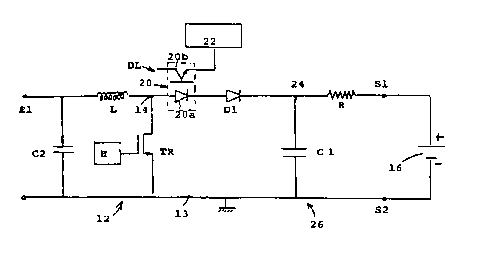
- figure 1 represents the wiring diagram of a logic input circuit ~oordirx,~
to the
invention;
figure 2 shows the wiring diagram of an alternative embodiment.
Description of a preferred embodiment
In figure 1, a logic input circuit 10 of electronic equipment for an
industrial automatic
control system comprises an input E1 connected to a voltage step-up energy
converter 12 comprising an inductance coil L associated to a switching
transistor
TR. The emitter of the switching transistor TR is connected to the input
potential
reference 13, and the collector is connected to the mid-point 14 of connection
of
the inductance coil L to a logic level detector DL. The base of the transistor
TR is
controlled by a clods drcuit H designed to perform voltage matching of the
input
signals by adjusting the frequency and duty cycle. It is thus possible to
apply
voltage values comprised between 24V and 110V to the input E1 depending
on the type of battery 16. The input potential reference 13 is at the
potential of
the negative pole of the battery ~ 6.
The logic level detector DL is formed for example by an optocoupling element
20 the receiver 20b whereof delivers a measurement signal SE to a data
acquisition circuit 22, said control signal SE being representative of the
logic state
on the input E1. The anode of the emitting diode 20a of the optocoupler 20 is
connected to the mid-point 14, whereas the cathode is connected to the
positive
pole of the battery 16 via a r~ecfifier diode D1 in series with a resistor R.
A first
filtering capacitor C1 is connected in parallel between the input potential
reference 13, and the mid-point 24 of oonnecction of the diode D1 to the
resistor
R. A second filtering capacitor C2 is connected between the input potential
reference 13 and the other input E1.
The rectifier diode D1, resistor R and first Tittering capaator C1 constitute
an
energy recovery circuit 26, the outputs S1 and S2 whereof arse connected ~
parallel to the terminals of the battery 16.

CA 02350664 2001-05-09
4
The switching transistor TR can be formed by a MOS, FET, IGBT, etc.
transistor.
The other logic input arcu'rts (not represented) are identical to the one
described
previously and are all connected in parallel to the terminals of the battery
16.
Operation of the logic input circuit 10 is as follows:
The elements of the logic input arcud 10, in particular the switching
transistor TR,
are dimensioned for the maximum Input voltage, for example 110V. The input
E1 can be voltage matched by adjusting the frequency of the dodo arcuit H and
by adjusting the duty cycle thereof. It thus enables the time during which the
switching transistor TR is fumed on and off to be adjusted.
In logic low state (0), the voltage applied to the input E1 is zero and tum-
off of
the diode D1 prevents any current flow in the inducfanoa coil L, whether the
transistor TR is on or off. The optocoupler 20 also remains off and there is
no
current flowing therethrough.
In logic high state (1 ), the voltage applied to the input E1 is appreciably
equal to
the voltage of the battery 16. When the transistor TR is fumed on, a current
is
established between the input E1 and the input potential reference 13 floHring
~
the induc~anoe coil L. After the transistor TR has switched to the off state,
the
inductance coil L generates a voltage surge at the terminals of the transistor
TR
and the potential of the mid-point 14 becomes higher than that of the output S
1
connected to the positive pole of the battery 16. A mean current of about lOmA
is then established in the direction of the battery 16, passing through the
resistor
R. Detection of the logic high state (1) is performed by transmission of the
measurement signal SE to the acquisition anaxt 22, which transmission is
performed with a very low heat dissipation, since most of the energy is
restored
to the battery 16 by the energy recovery circuit 26.
The voltage increase at the mid-point 14 is relatively low to preserve a good
efficiency, but sufficient to ensure flow of the mean current of 10 mA. The
value of

CA 02350664 2001-05-09
the voltage increase is a function of the duty cycle of the transistor TR, end
enables the logic input circuit 1 D to work in constant current regardless of
the input
voltage. The terminal of the transistor Tf~ opposite the mid-point 14 is
advantageously at the input potential reference, which simplifies simultaneous
5 control of several transistors in case of a plurality of logic inputs in
parallel.
With reference to figure 2, the optocoupler 20 is removed from the front end
to
the DC side being electrically connected between the resistor R and the D C
voltage source 16.

Representative Drawing
A single figure which represents the drawing illustrating the invention.
Administrative Status

2024-08-01:As part of the Next Generation Patents (NGP) transition, the Canadian Patents Database (CPD) now contains a more detailed Event History, which replicates the Event Log of our new back-office solution.

Please note that "Inactive:" events refers to events no longer in use in our new back-office solution.

For a clearer understanding of the status of the application/patent presented on this page, the site Disclaimer , as well as the definitions for Patent , Event History , Maintenance Fee  and Payment History  should be consulted.

Event History

Description Date
Application Not Reinstated by Deadline 2006-09-08
Time Limit for Reversal Expired 2006-09-08
Inactive: IPC from MCD 2006-03-12
Inactive: Abandon-RFE+Late fee unpaid-Correspondence sent 2005-09-08
Deemed Abandoned - Failure to Respond to Maintenance Fee Notice 2005-09-08
Letter Sent 2001-11-30
Inactive: Single transfer 2001-10-22
Inactive: Cover page published 2001-09-21
Inactive: First IPC assigned 2001-08-02
Inactive: Courtesy letter - Evidence 2001-07-24
Inactive: Notice - National entry - No RFE 2001-07-18
Application Received - PCT 2001-07-16
Application Published (Open to Public Inspection) 2001-03-22

Abandonment History

Abandonment Date Reason Reinstatement Date
2005-09-08

Maintenance Fee

The last payment was received on 2004-09-03

Note : If the full payment has not been received on or before the date indicated, a further fee may be required which may be one of the following

  • the reinstatement fee;
  • the late payment fee; or
  • additional fee to reverse deemed expiry.

Please refer to the CIPO Patent Fees web page to see all current fee amounts.

Fee History

Fee Type Anniversary Year Due Date Paid Date
Basic national fee - standard 2001-05-09
Registration of a document 2001-10-22
MF (application, 2nd anniv.) - standard 02 2002-09-09 2002-08-12
MF (application, 3rd anniv.) - standard 03 2003-09-08 2003-07-30
MF (application, 4th anniv.) - standard 04 2004-09-08 2004-09-03
Owners on Record

Note: Records showing the ownership history in alphabetical order.

Current Owners on Record
SOPRANO
Past Owners on Record
OLIVIER FRANCOIS
PATRICK PIRON
RICHARD DREVON
Past Owners that do not appear in the "Owners on Record" listing will appear in other documentation within the application.
Documents

To view selected files, please enter reCAPTCHA code :


To view images, click a link in the Document Description column. To download the documents, select one or more checkboxes in the first column and then click the "Download Selected in PDF format (Zip Archive)" or the "Download Selected as Single PDF" button.

List of published and non-published patent-specific documents on the CPD .

If you have any difficulty accessing content, you can call the Client Service Centre at 1-866-997-1936 or send them an e-mail at CIPO Client Service Centre.


Document
Description 
Date
(yyyy-mm-dd) 
Number of pages   Size of Image (KB) 
Representative drawing 2001-08-27 1 5
Abstract 2001-05-09 2 80
Description 2001-05-09 5 198
Claims 2001-05-09 2 59
Drawings 2001-05-09 1 13
Cover Page 2001-09-18 1 38
Notice of National Entry 2001-07-18 1 194
Courtesy - Certificate of registration (related document(s)) 2001-11-30 1 113
Reminder of maintenance fee due 2002-05-09 1 111
Reminder - Request for Examination 2005-05-10 1 116
Courtesy - Abandonment Letter (Request for Examination) 2005-11-17 1 167
Courtesy - Abandonment Letter (Maintenance Fee) 2005-11-03 1 176
Correspondence 2001-07-18 1 24
PCT 2001-05-09 4 129
Fees 2003-07-30 1 27
Fees 2002-08-12 1 30
Fees 2004-09-03 1 29