Note: Descriptions are shown in the official language in which they were submitted.
CA 02350879 2001-07-05
- 1 -
RADIOTELEPHONE S''STE!"I FOR. GROUPS OF REMOTE SUBSCRIBERS
Field of the Invention
This invention relates to radiotelephone systems for
serving a plurality of remote subscriber stations and, more
particularly, to a radiotelephone system in which certain
of said subscriber stations are located in a physically
adjacent group.
Backcrround of the Prior Art
A radiotelephone system including a base station for
serving remote subscriber stations is described in U.S.
patent 5,119,375. In that system each subscriber station
was equipped with a radio that could be instructed by the
base station to tune to a particular channel and to employ
a particular time slot for the duration of a given
conversation. Time division multiplex (TDM) radio channel
transmission was employed from the base station to the
subscriber stations and time division multiple access
(TDMA) transmission from the individual subscriber stations
to the base station. The time division of each radio
channel into time slots and the compression of speech
signals permitted each radio frequency channel to support
a number of voice paths equal to the number of time slots.
Analog, voice signals to and from the public switched
telephone network were first converted to 64 kbps ,u-law
companded pulse coded modulation (PCM) digital samples.
Before transmission over the radio channel the digital
samples were subjected to voice-compression to reduce the
voice information rate from 64 kbps to 14.6 kbps using
residual excited linear predictive (KELP) coding. A voice
codec and modem were required to be dedicated to a specific
frequency and time slot for the duration of a call.
While the foregoing system operated in a highly
satisfactory manner in allowing telephone service to be
provided especially to areas where wire lines are
CA 02350879 2001-07-05
=2-
impractical, the unforeseen growth of such telephone
service has given rise to sitii~tions iii which several
subscriber stations are found to :Lie in close proximity
with one another. Initial efforts to lower the per-line
cost of serving a group of~such closely situated subscriber
stations were focused on consolidating the~installation and
maintenance costs of individual subscriber stations~through
the sharing of common equipment such as the enclosure,
power supply, RF power amplifier and antenna. Thus, in a
closely situated group of subscriber stations, each of
which could access an RF channel, a single broadband RF
power amplifier could be employed to serve the group.
However such efforts still required each subscriber line to
have its own modem anc~ radio transceiver. ' ~'he individual
transceiver outputs were fed, to .the common RF power
amplifier, which had to be designed to handle a peak power
equal to the sum of the power of ell of the. transceivers in
the group of adjacent eubecriber~ stations~~that could
simultaneously be active on the~.eame time slot. It is
2o apparent that further consolidation over that possible in
the '375 patent system and a reduction~~in the~peak and
average power required would be..desirable, especially in
remote areas recxuired to be served by~solar cell power.
Summary of the Invention
2S - In accordance with the principles of our invention,
per-line costs are reduced for a physically adjacent group
of subscriber lines by pexznitting~ the lines within such a
group to share not only a common power~supply and RF power
amplifier, but modem, synchroniaation,~ IF, up-and down-
30 conversion and controller functions as well,' so that
significant concentration is achieved. In our system, a
small number of modems is provided to serve the multiple
subscribers in a physicallyadjacent group, hereinafter
referred to as clust2r or, more part:icUlarly, as a modular
35 cluster. In an illustrative embodiment, subscriber line
CA 02350879 2001-07-05
-3-
circuits and modems are modularized printed circuit cards
which plug into a frame employing backmlane wiring to
dvst~-ibtrt~ t~mir.g _n~orna~i~:~ and :iota amor_g ~.~-:e a~:i~s .
Ar_y o= the modems may be seized to handle a call for any of
the subscribers and each modem may handle calls for several
subscribers on successive time slots. The same or a
different freauer_cy may be used to support communicatior_s
for each subscriber on successive time slots.
It is a feature of our invention that the selection
from the common pool of frequency-agile modems of the modem
to be used to handle a call is controlled to conserve Dower
consumption in two ways. First, a new modem is preferably
not seized fog use to handle a call until all of the time
slots on active modems have been assigned to calls, thereby
allowing all not-yet-selected modems to remain in a power-
conserving, "powered-down" state.
Second, the number of calls using the same time slot (on
different frequencies) is controlled to reduce the peak
power demand on the RF power amplifier.
It is a further feature oz our invention to avoid
synchronization delay when it is necessary to seize a
powered-down modem for use on a call. Once time slot
synchronization with the base station has been established
for the first modem of the pool at the cluster,
synchronization infornation is made available to the
remaining modems, advantageously over backplane wiring,
under control of a microprocessor-based cluster controller.
Accordingly, all powered-down modems remain instantly
assignable to handle calls without undergoing any delay to
become synchronized with the base station's time division
frame.
It is a further festur' of our invention to classify
modem synchronization states according to several
sv-ichronizaticn parameters and to deri~r4 a confidence
factor ,-__or each active modem that reflects the reliability
of the synchronization parameters and to distribute
CA 02350879 2001-07-05
-4-
s~nchtonizatiori information trorti the modem haling the best
confidence factor.
Briez Description of the Drawings
The foregoing and other objects and features of our
S invention may become more appareht by referring now to the
drawing in which
Fig. 1 is a block diag~-aM of a Modular cluster having
a common pool of frequency agile modems for handling a
group of subscriber stations;
Fig. 2A shows the association'of subscriber line
circuits and Modems at the time slot iriterchanger;
Fig. 2H shows the TDMA RF frame allocated for 15PSK
time slot ; ~ '
Fig. 2C shows the TDMA RF frame allocated for QPSK
time slots;
Fig, 2D shows the task scheduling between the TDMA
time slots and the PCM buffers;
Fig. 3 shows the principle circuit elements of a
frequency agile modem module;
2~ Fig. 4 shows the IF portion afwthe frequency agile
modem;
Fig. 5 is a block diagram of the block synthesizer,
up/down converter;
_" Fig.~6 shows the frequency synthesis and noise shaper
for the receiver portion of the modem;
Fig. 7 shows the frequency synthesis, modulation and
noise shaper circuitry for the IF'transmitter portion of
the modem; arid
Fig . B shows the system clock generation circuitry for
the modular cluster.
General Description
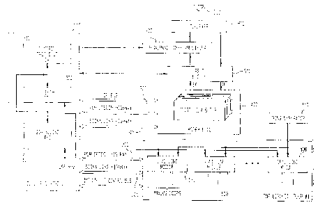
Fig. 1 is a block diagram of a modular subscriber
cluster that is located rAmotely from a base station (not
CA 02350879 2001-07-05
_S-
shown). The subscriber cluster is termed "modular" because
the line circuits 100 and the modens 400 are comp=iced of
plue-in units . accord-ng'~y, the ruT~er cf p 1 ugaed-
subscriber line circuits 100 will depend on the number o=
subscribers in the local i ty ar_d the r_umber of pl ugged-in
modems 400 may be traffic-engineered to handle the amount
of traffic expected to be generated by the number oz line
circuits 100. Line circuits 100 are contained on quad line
module cards 101-108, each of which serves four subscriber
lines. Eight such quad lire module,; provide loop control
functions to a line group of 32 subscriber lines and
circuits 100 may cor_tain multiple line groups.
Each lire circuit on each quad line module 101-108 is
given a dedicated PCM time slot appearance in PCM speech
1S highway 200 and in signaling highway 201. The quad lln~
modules 101-lOB include voice codecs (not shown) to encode
subscriber loop analog voice onto PCM data highway 200.
Subscriber loop signaling information is applied to
sigr_aling highway 201 by a subscriber line interface
circuit SLIC (not shown). Either ~C-law or A-law PCM coding
may be used.
The connection of a particular one of modems 400 to
handle a call from or to a particular one of the line
circuits on one of quad lire modules ? O1-108 is made via
2~ time slot interchangers 310 and 32.0, as instructed by
cluster controller 300. PCM data time slot interchanger
320 conveys speech samples between the PCM speech highway
200 serving Line modules 101-108 and the Pr'M speech highway
220 serving modem pool 400. Signaling time slot
ir_terchanger 310 conveys signalling information between
signalling highway 201 serving the modules 100 and
signalling highway 221 sensing modem pool 400.
Two RF channels are required for a telephone
conversation, one for transmissions from the base station
~o the subscriber (the 'forward' channel) and one from the
subscriber to the base station (the 'reverse' channal).
The forward and reverse channel frequencies are assigned by
CA 02350879 2001-07-05
-6-
the telecoinmun~catione authox'ity and in a typical example
may be separated from each other by 5 MHz. The path of tine
forward channel radio 9igr_al received at the cluster from
the base station may be traced ftoni c:ltister antenna 900 and
duplexer B00 to block synthesizer up/down converter (BSUD)
600: In block converter 600 the RF signal is limited,
band-pass filtered and down-converted from the 450 MHz, 900
MHz off- other high, or ultra-high frequency RF band to an IF
signal iri the 26 - 28 MI-~z range . The IF signal is
l0 delivered to modems 400 which process the signal for
delivery to the subscriber line circuits via the time slot
interchangers in the cluster controller 300:
. The modems each include a baeebarid~digital signal
processor (see Fig. 3, DSP/HH) and a rridderri' ~rocesaor (gee
Fig: 3, DSP/MDM?: In the for4iard channel direction; modem
processor DSP/MDM demodulates the IF signal received from
bloclt Converter 600 and transfers the data to baseband
prdcesaor DSP/BB which expands the demodulated data into ~e-
law or A~law eilcoded signals for transmission through time
slot interchanges 320 to the line modules: The modem's
baseband processor DSP/BB interfaces to modem processor
DSP/MDM vie ~ direct memory access (DMA) interface (see
Fig. 3) and to the PCM highways through the processor's
serial port. In the reverse channel direction, baseband
processor DSP/BB con~tterts the u-laai or A-law coded PCM
inforc~tation received from PCM highway 500 into linear form,
compresses the linear data using'~RELP coding and DMA
transfers the compressed data to digital signal processor
DSP/MDM which modulates the sigilal far transmission on the
radio channel time slot:
As shown W Fig. 2A, each -of inodecris 400 and each of
line modules 100 has four dedicated time slot appearances
in PCM data time slot interchanger-320 for non-blocking
access. Each modern is assigned two adjacent PCM slots in
PCM time slots 0-15 and two adjacent PCM time slots in PCM
time slots 16-31. As an example, for a particular call,
TSI 320 connects line circuit 0 of line'module '101 to
CA 02350879 2001-07-05
_7_
channel 1 of modem 1, and line circuit 1 of line module 101
is connected to channel 0 of modem 1, and so on. Time slot
ir_t°-rchancers 31C; anc 320 p~ov=de a repetitive 125 ~.r,S
sampling period containing 32 time slots operating at a
S rate of 2.o4s Mbits/sec. During each I25 ~S PCM interval,
the line modules may send thirty-two, 8-bit bytes of data
to time slot interchanges 320 and each modem may receive
four of the 8-bit bytes at its baseband processor serial
port, packed together as two 16-bit words. Each 16-bit
to word causes a aerial port interrupt on the baseband
processor. When the interrupt is received, the baseband
processor determines whether the pair of PCM samples
contained in the l~-bit word correspond to slots 0 and 1 or
to slots 2 a_nd 3. Similarly, during each 125 ACS PCM
15 interval, four voice channels of PCM data, packed together
as two I6-bit words, may be sent. from each baseband
processor's serial port to time slot intercha_nger 320 for
delivery to the line modules.
The TDM (RF) frame at the base station is shown in
20 Figs. 2B and 2C, each having a duration, illustratively, of
45 ms. The 16PSK frame of Fig. 2B has four time slots,
each of duration 7, each time slot capable of carrying the
different frequencies assigned to the forward and reverse
channels of the call. In Fig. 2C the RF frame of the same
25 duration is capable of accommodating the forward and
reverse channels of two QPSK modulated calls. It can be
appreciated that, alternatively, the TDM frame can carry
four 16PSK calls or two QPSK modulated calls.
Fig. 2D illustrates the timing of the tasks performed
3o at the cluster in conveying information between an
illustrative TDMA frame carrying QPSK modulated calls and
the DCM highway frames. Line (1) represents the buffers for
recAiving the two QPSK modulated forward channel time
slots, R:{1 and Rx2, of the TDh~ frame. Demodulation is
3J begun as soon as the receive buffer has received the rust
half, Rxla, of the time slot. Line (2) represents the
buffers preparing to transmit in the. two reverse charnel
CA 02350879 2001-07-05
-8-
QPSK time slots, TxI and Tx2, of a TDMA frame. Note that,
at the cluster, the reverse channel time slots are offset
from the forward channel time slots so that the eubscz~iber
station may avoid the expense and bulk of a duplexer. In
addition, the subscriber unit's the reverse channel c.till be
offset so that it twill be received at the bade station at
the proper time taking into accotiht 'the' distance between
the subscriber station and the base Station, Lines (3) and
.. , (4) of Fig, 2D represent the buffers in the .Stmt (Fig. 3)
IO of the modem which store the PCM iaords to and from speech
time slot interchanger TSI 320 (Fig. 1).
In normal voice operation, the modem processor DSP/MDM
demodulates received forward channel symbols, packs them
into a buffer ~n SRAM/MDrt ~.nd sends the contents of the
buffer to the baseband procesaof DSP/BB for KELP synthesis
(expansion): The baseband processor encodes the expanded
data to ~1-law or A-laW and puts it on the PCM bus for
delivery to the line motiuleg. Voice code words are
transmitted iii every frame during active vbice operation.
The code t~ord r~s~des at the beginning of the burst between
the preamble and voice data on both the forward and reverse
channels. The forward channel voice code words contain
information that may be used to adjust transmit power and
timing. Local loop control information (i.e.,~ onhook,
' 25 offhook, ring, forward disconnect) is also embedded in
these code ~iords. The reverse channel code words contain
subscriber station local loop control and forward channel
link quality information.
The fortdard voice codewotd i5 decoded by the modem
processor DSP/MDM. The forward voice codeword contains
transmit fractional timing contfol,'transmit power level
control and local lbop control information: The fractional
timing and power level control irifox-mation is averaged out
over a frame and the average adjustment made at the end of
the frame. The local loop control information i9 stored
locally and changes in loop state are detected and reported
to the cluster controller. The local loon control also
CA 02350879 2001-07-05
_g_
causes the modem to Send out line circuit control over the
signallir_g bus. The reverse voice codeword contains local
loop status that i~~ used by the cluster cone-oiler ar_c base
station to monitor call progress.
The modem processor DSP/MDM performs receive FIR
filtering and automatic gain control of the received
samples during a receive symbol interrupt service routine.
The demodulator routine in the modem processor is called
when half a slot of baseband information has been received
in the receive buffer. The demodulator operates on the
half slot of data and passes the packed output data to the
baseband processor DSP/BB for RELP synthesis. Data
transfer to and from the baseband processor is controlled
so that the ?2ELP input queues are filled before tine
corresponding synthesis data is requ~.red, and RELP output
quet:es are emptied before r_ew analysis (compression) output
data arrives. During demodulation, automatic frequency
control (AFC), automatic gain control (AGC) and bit
tracking processes are performed to maintain close
2o syr_chronization with the base station.
It should be appreciated that mixed mode operation is
possibl a whereby some time sl ots in the RF may employ lo'PSK
modulation while the remaining slots employ QPSK
modulation.
Synchronization to the Base Station
Before an RF channel can be used for communication
between the base station and the cluster, the cluster must
be synchronized to the RF time slot scheme used by the base
station (not shown). In accordance with our invention, one
or more of modems 4oo will be ordered by cluster controller
300 to acquire synchronization with the base station RF
frame timing by searching for the channel frequency
carT-ying the radio control ciian~wel (RCC) being used by the
base station. Clu;>ter controller 300 includes a master
3~ control microprocessor 330, illustratively, one employing
CA 02350879 2001-07-05
-10-
a Motorola 58000 series processor, which ~eendg control
information over ~.he CP bus to the micz'oprocessors in
modems 400. On power up, cluster controller 300 down-loads
appropriate software and initialization data to modems 400.
S After the channel frequency is found; the modem must
synchronize with the base station time slot by decoding the
RCC unique word: As described in the aforementioned '375
patent, the RCC channel i9 distinguished from other
channels in that it has an extended guard interval: during
its time slot and includes a DBPSK modulated'unique word of
8 bits. In order to minimize the possibility of aborting
a call if the modem with the active RCC time slot fails and
it becomes necessary to assign the RCC time slot to a
different modem, time slots are assigned within an active
modem Bo that the synchronization (RCC) tirrie~ slot (referred
to as Rx0 where the four time slots axe numbered . Rx0
through Rx3, or Rxl. where. the ' time slots are number Rxl
through Rx4); is the last to be'filled:
At start-up, all of fiodecris 400 are assumed to be out
of synchronization with the base station's RF 45 rris frame.
During tune slot zero of the RF frsme,~the base station
transmits an RCC message on some RF channel which;'when
received at the modular cltister,~will be decoded to~put the
cluster into synchronization with the base station's RF
time slot frame for all RF channels. Until synchronization
with the base station is achieved, each modem generates its
own local RF frame sync. Cluster controller 300 next
commands one or more moderns to hunt for the RCC transmitted
by the base station on different RF dhannel~ until the RCC
is found or all channels have- been sea~th~d. If all
channels have been searched and the Rc:C has not been found,
the controller orders the search to begin again.' When a
modem finds the RCC, the controller designates it as the
RCC modem and distributes its sync inforni~tion to the
remairiing modems vii the frame sync signal over the
backpiane:
CA 02350879 2001-07-05
-11-
when the RCC slot search is undertaken, the channel
number is used by the modem to digitally sweep a d=rct
digital rrequency s;rnthes~.s (DDFS; local oscillator ,
illustratively over a 2 N~:z range. There are two stages to
a modem's acquisition ef the RCC channel, coarsely
identifying the center frequency and finding the "AM hole",
a portion o= the RCC time slot where the number of symbols
transmitted by the base station does not fill up the entire
slot time- Coarse frequency acquisition is based on
performing a Hilbert transform of the spectrum of the RCC
channel which yields a frequency correction for the local
oscillator. This continues until the energy in the upper
half of the spectrum approximates that in the lower half.
After coarse frequency acquisition is obtained,
illustratively to within an accuracy of 300 Hz of the
channel center frequency, a search is made for the AM hole.
A number of null signals are transmitted prior to the RCC
data. The AM hole is identified by monitoring tile
amplitude of consecutive received symbols. when twelve
consecutive null symbols are detected, an AM strobe signal
is output by the modem to indicate the start of an RCC slot
and the start of a TDMA frame. This coarsely synchronizes
the baseband modem timing to the base station timing.
Synchronization need only be performed once since the radio
link is shared by all baseband modems in the modular
cluster. The frame sync signal is sourced by one modem to
all other modems in the cluster via a signal on the
backplane wiring. During the search for the RCC if the AM
hole is found to within 3 symbol periods of the start of
frame marker, coarse acquisition is complete. The location
of the unique word within the frame provides the modem with
timing information that is used to bring the modem's local
frame timing to within one symbol timing of the base
station. 'he modem is said to be in receive sync, Rx RCC,
3S as long as it continues to receive and decode the u_niaue
word correctly. Once synchronization is achieved, 16PSK
modulation cerresoonding to 4 bits per symbol, QPS~C
CA 02350879 2001-07-05
-12-
modulation cotresponding to 2 bits per symbol, or
combinations of botfl may be employed.
While all modems are capable of receiving and
synchronizing to the base station's radio control channel
RCC, only one modem need do this since the modem which is
selected by the cluster controller can share its timing
with the other modems via the Frame Sync signal over the
l~ackplane wiring. The selected modem will source the Frame
Sync Out signal and all other modems will accept this
signal as the Frame Sync In signal.
When a modem goes on line, its modem processor DSP/MDM
instructs its DDF 4S0 (Fig. 3) to try to synchronize its
local frame timing to the backplane signal. Each modem's
DDF 450 timing is at this moment independent of every other
modem's timing. DDF 45o will initially be instructed by
its DSP%MDM to look at the backplane signal for its
-. synchronisation. If a backplan~ synchronization signal is
present, the DDF will synchronixe its frame sync signal to
the backplane signal and then disconnect from the backplane
signal. The backplane signal thus does not feed directly
into the modem's timing circuitry but merely aligns the
modem's internal start of recef~re frame Hignal. If a
backplane synchronization signal was not present, it is
assumed that the modem is the first one that has been
~ activated by the cluster controller, in which case the
cluster controller 300 will instruct the modem procpseor
DSP~MDM to look for the RCC and fend the modem's timing to
the cluster controller. '
Cluster cont oiler 300 next instructs the modem
processor D5?~~MDM to demodulate the DHPSK signal on the RCC
cha=rnel. The path for demodulation of the ~IF signal
received from block converter 500 may be traced to the
modem IF modtt?a where it is again band-pass filtered and
down-converted to a 16 kilosymbol peg second information
stream. The DHPSK modulation that is employed on the RCC
channel is a one bit per symbol modulation- The RCC
messages that are received from the base station must be
CA 02350879 2001-07-05
1 _W
demodulated and decoded before being sent to the cluster
controller. Only messages that are addressed to the
cluster controller, have a va l id CRC a~: a=a a burst -yr~e
message or an acknowledgment message are forwarded to the
Controller. A~._L other messages are discarded.
acknowledgment message signifies the correct reception of
the previous RCC message. A message is addressed to the
cluster controller. if the Subscriber Identification number
(SID) contained in the message matches the SID of the
IO cluster.
Referring to Fig. 3, the 16 kilosyrtbol per second IF
sigr_al from the fF circuitry of Fig. 4 is entered into A/D
converter 804, which is sampled at a 64 KF-~z rate by a clock
sigr_al received from DDF chip X50. A/D converter 804
15 performs quadrature band-pass sampling at a 64 kiiz sampling
rate. Quadrature band-pass sampling is described, inter
alia, in US patent 4,764,940. At its output, converter 80a
provides a sequence of complex signals which contains a
certain amount of temporal distortion. The output of
20 converter 804 (Fig_ 8) is entered into R.~cFIFO in DDF chip
450. Modem processor DSP/MDM reads the contents of R~cFIFO
and performs a complex FIR filtering operation, which
removes the temporal distortion introduced by the
quadrature band--pass sampling. After tine removal oz
25 temporal distortion, the signals are demodulated by
procssor DSP/MDM.
During the demodulation of RCC messages, AFC, AGC and
bit tracking processes are perfomed by modem processor
DSP/MDM to maintain the cluster in close synchronization
30 with the base station. Transmit timing and power level
adjustments are made according to information received in
the RCC message. Processor DSP/MDrt examines the
demodulated data and detects the RCC message, a message
~.vhich includes link status bits, and 96 bits of data that
3includes the subscriber ID. Modem pz-ocessor DSP/MDM also
recognizes whether the subscriber ID belongs to one of the
subscrii~er line circuits in the cluster.
CA 02350879 2001-07-05
_,
tf,.th~ m~s~age is fo,f this clust~r,"'th~ me~g~ge is
passed to cluster controllef 300, which. interprets the RCC
command. Forward RCC messages include page message, a call
connect, clear indication and self=test. Reverse RCC
S messages include call accept, clear request,'test results
and tall request: If the RCC triessage is ~a pale message;
the cluster controller for which it is designated will
formulate a call accepted message to be~ transmitted back to
the base station: From the call accepted in2g9age the base
station determines the timing offset between the cluster
and the base station and the base station sends symbol
timing update information to the cluster in the next RCC
message, iahich is the call connect message:
When the RCC message is a call Connect m~ss~:ge, the
' information therein instructs the cltiatez- controller what
adjustment to make in symbol timing,' whether to adjust
power level , fractional timing, and what channel to use for
the remainder of the call (chaninel htimber, TDM slot number,
whether QPSK or 16PSK mod~ilation wi~l be employed~and what
the subscriber line type ie): ~ '
The first modem which hag found the RCC is designated
the RCC modem and its frequency offsetj~ receive gain
control Rx AGC, and start offrame information i9
coilsidered valid and may be dist~ibiited to the other
modems. The cluster controller recei~es'the channel riumber
information and decides which modem is to be in~t.nlcted to
tune ui~ to the designated channel to handle the~remainder
of the call.
The firial~~tep toward total s~nchxonization is the
s~icce~sful establishment of a voice Channel. When a lroice
chanriel is established the last' two synchronization
parameters become valid' the tranazriit,symbol timing and
transmit symbol fractional timing, At this point; should
another modem be activated by the cluster controller all of
the necessary synchronization irifc~-trixtion is aliailable to
be provided to the modem, making the establishment of a
voice channel much. easier and clicker. A confidence level
CA 02350879 2001-07-05
-15-
is calculated to evaluate the synchronization infoz-~nation
of each modem. The cluster controller upda~es the
COnLl~°_::C°_ lE?Vel LOr eaC:_ IT:Cd°,T:
W~1~°_n:yt~or t;:ero 1S 3 Cr:aI-'_Ce
in sync status, link cruality, or receive AGC. The cluster
controller finds the modem with the highest confidence
level and distributes its synchronization parameters to the
remaining modems.
When a modem slot is commanded to enter the voice mode
by tile cl uster controller, the modem first atterrn_ is to
perform refinement. Refinement is t=he process of finely
synchronizing the modem's transmit timing and power level
to the base station's receive timing. The refinement
process is controlled by the base station. The base
station and the modem exchange special refinement bursts
until the base station terminates the refinement process
when the predetermined degree of synchronization has been
achieved. The modem then goes into normal voice operation.
If the base station aborts the refinement process, the
modem will abort the call, go into the idle state and
inform the cluster controller. Refinement bursts are DBPSK
bursts formatted like RCC bursts. Refinement bursts are
detected by the presence of a unique refinement word. The
modem is said to be in voice synchronization when the
refinement unique word is detected with zero offset. The
forward and reverse voice codewords have a voice codeword
check byte attached for error detection. The modem will
report a loss of sync if 9 consecutive frames are received
with voice codeword errors, at which time the cluster
controller enters the recovery mode until a good codeword
is found or until the modem is commanded out of this mode
and placed into idle mode.
Based upon the synchronization state, cluster
controller 300 determines the validity of the
syr:chror_ization parameters provided by the modem. The
table below shows which parameters a_-e valid, based upon
the cure=nt synchronization state of a modem. An °X" in
the box indicates that the parameter i.s valid.
CA 02350879 2001-07-05
-is-
Sync State Freq. Sy bol Fract. TxPLC RxAGC SORF
Offset Time Time
No sync
px syr~c~~cc) X ', x x
Tx Sync (pCC) X X X X
Voice sync X X X X X X
A 12-bit confidence factor word ig computed by the
modem to reflect the reliability of the synchronization
parameters ascertained by the modem. The confidence factor
word is assembled by concatenating the bits representing
the voice and receive sync statee.of the modem with bits
identifying the link quality and receive AGC parameters,. as
set forth in the following table:. .
Bit Allocation 1 t 10 9.:8 7..0
Field Voice SyncRz SytiC(RCC)Link Quality~tiAGC
The single bits 11 and 10 identify, respectively,
whether or not the modem is in voice sync and receive sync .
The two bits 9 and 8 udentify ' foU.r ' grsdations or - link
quality, while the 8 bits allocated to receive ~GC level
indicate the level of gain required:
~2 0 MODEM MODUL)J ; FIG : 3
The principle components of the ctiodem module are shown
in Fig. 3. The modem module ~dan support up to four
simultaneous full duplex voice channels. The processing to
dynamically handle all functions required by an active
channel is partitioned betWedn the Bluster controller
processor 320, (Fig: 1}, and proce~~sors D5P/MDM and DSP/BB
in each modem f'~ig: 3). The clu~teY controller handles
higher level functions incli.idiizg call set=Lip, channel
allocation and system control: '~ Modem processor DSP/MDM
CA 02350879 2001-07-05
-17-
handles filtering, demodulation and routing or the incoming
radio signals, fo=-matting of data oe~o~e t-ans;nissio;z over
the radio channe ~ , and managemer_t o= data =low ~,etween
itself and baseband processor DSP/BB. Basebar_d processor
DSP/BB performs the computationally intensive tasks o=
voice compression and expansion and, in addition, handles
the PCM bus interface. Tn normal voice operation, modem
processor DSP/MDM demodulates received symbols, packs them
into a receive buffer and sends the voice data buffer to
baseband processor DSP/BB for RELP synthesis and
transmission to the subscriber lire c~'_rcuit over the PCM
bus. The modem processor DSP/MDM also accepts compressed
speech from baseband processor DSP/BB, formats it into TDMA
bursts and sends it to the transmit pulse shaping filter
FIR contained in DDF 450 for transmission over the radio
link. The modem operates on both QPSK and 16PSK
modulations (and DBPSK during refinement) under control of
the cluster controller.
Processors DSP/BB and DSP/MDM each have a dedicated
2o random access memory, SRAM/MDM and SRAM/BB, respectively.
However, modem processor DSP/MDM may request access to the
random access memory SRAM/BB by activating its DMA HOLD
output and obtains such access using the data and address
bus when the baseband processor DSP/BB activates its DM.A
ACK output signal.
Assignment of Time Slots
As described in the '375 patent, the RPU in the base
station keeps track of , the radio channels and time slots
that are in use and assigns both the frequency and the time
slot to be used on any ca?1_ A slot is selected which is
in use by the least number of calls so that the call
traf f is can be more evenly distributed acr oss aI l s 1 ots .
HoweveY, in accordance with that aspect of the present
invention which is- concerned with minimizing the power
3s expended at the remote modular cluster, calls are assigned
CA 02350879 2001-07-05
-18-
so as to (a) minimize the number of active modems and (b)
control the number of conversations simultaneously using
the same time slots. ;urther, while it is desirable to
employ 16PSK modulation in every ts.me slot of a TDMA frame
so that four complete calls can be accommodated, it i9 also
important to permit QPSK calls to be made and to keen an
alternate RCC slot available for synchronization purposes.
Accordingly, the cluster and the base station must
cooperate in the assignment of tittle slots to achieve these
goals. The cluster keeps track of available time slots and
the type of modulation being employed on each slot . The
cluster then assigns priority levels to each available slot
and maintains a matrix of priority values which takes into
account the factors that (a) an alternate receive time slot
(generally the first time slot) on.some channel must be
allocated for RCC synchronization, (b) adjacent time slots
should be left available as long as possible so that QPSK
calls can be handled if necessary, and (c) time slots
should be assigned to handle calls without, iz possible,
activating a powered-down modem or assigning a slot that is
already in use by a large number of other calls: The
routine (in pseudo code) for achieving these goals is as
follows:
Prioritize Siot Routine
2 S List 1 = alt idle time slots available on already active modems for 16f5K
calls
and QPSK calls;
List 1 A = ail idle modems;
List 2 = Llst time slots whose use wilt not exceed the thi~eshhold number of
calls using the same time slot In the cluster,
3 0 ~ List 2A = List 1 minus Llst 2;
List 3 = List 2 minus time slots on modems having adjacent time slots
available (for pPSK caNs);
List 3A = List 2 minus time slots on modems nol having adJacent time slots
available (tor OPSK calls);
CA 02350879 2001-07-05
9_
List 4 = List 3 minus time slots on modems not having a synchronization time
slot available (slot 0 for the RCC);
List 4A = List d minus time slots on modems having a synchronization time slot
available;
Mark list 4 as first choice;
Mar',t list 4A as second choice;
Mark list 3 as third choice;
Mark list 3A as fourth choice;
Mark list 2 as fifth choice;
~ Mark list 2A as sixth choice;
Mark list 1 as seventh choice;
Mark list 1 A as eighth choice.
The above Prioritize Slot Routine is called whenever
the cluster receives an RCC page message from the base
station or is about to formulate a call request message to
the base station. When the base station responds with a
call conr_ect message containing the frequency, type of
modulation and time slot to be used, the cluster once again
performs the Prioritize Slot Routine to see i= the slot
2Q selected by the RPU is still available. If still
available, the slot is assigned to the call. I-iowever, if
in the meantime the slot assignments have changed, the call
will be blocked.
An example of how the Prioritize Slot Routine is
executed under light and heavier traffic conditions may be
helpful. Consider first the following table, which
illustrates a possible condition of the modems and assigned
time slots under light traffic conditions, just before one
of the subscribers served by the modular cluster initiates
a request for service:
CA 02350879 2001-07-05
CJ -
Modem Time Slot
'
0 1 2 _ _
0 RCC 16PSK
1 16PSK ~PSK OPSK
Z IDLE IDLa= IDLE IDLE
S 3
The above table indicates that modem 0 has slots 2 and
3 available, that modem 1 has slot 1 available and that
modems 2, 3 , 4 and S are powezed-down, ail of their : time
slots being idle. 'rhe cluster executed the Prioritize'Slot
Routine which determines that slots 1, 2 and 3, in that
order, az~~ the preferred slots to be assigned to handle the
next 15PSK call and that for QPSK calls the preferred slots
are 2 and 0, iri that order. The cluster then sends ~ "call
request" signal to the base station using the RCC word and
iriforzns tile b~.se station of Ehis pr~~erence . In the table
belo:v the rationale for etch of the priorities is set
forth
2 0 Slot PriorityRaiional8 Slot PriorityRationale
ltSPSK t7PSK
1 No new modems to power 2 (Same reason
up; as
no (hcraas~ iri in3x ~ iSPSK for
slot activity; slots
OPSK sots 2.3 kept available;~ . 2,3}
RCC slot available.
2 New ~PSK call requires 0 Requires new
new
modem power up. ~ modern power
up
' 3
2 S D flequires new modem
power up.
Another example may be helpful. Consider the status
of time slots among modems 0-5 under somewhat heavier
traffic conditions, as shown in the following table,
wherein empty boxes indicate idle time slots:
CA 02350879 2001-07-05
-21-
Modem Tirne Slot
0 - ~ ~
0 RCC 16PSK QPSK QPSK
1 QPSK QPSK I 16PSK
16PSK 16PSK 16PSK
3 I c.3PSK ~ QPSK QPSK (~PSK
4 16PSK 16PSK 16PSK
S 16PSK
The slots to be assigned set forth
are i:~
the
following table together i
with t'r?
e rat onale:
Slot PriorityRationale Slot PriorityRationale
18PSK QPSK
3 No new modems to power 2 only choice
up;
max slot activity avoided;
OPSK slots 2.3 kept
available;
RCC slot kepi available.
2 No new modems to power
up;
max slot activity avoided;
RCC slot kept avaiiabie,
BUT,
new OPSK call requires
new
modem power up.
1 No new rnadems to power
up;
QPSK slots 2.3 kepi
available;
RCC slot kept available,
BUT
max slot activity exceeded.
0 No new modem power Up;
QPSK slots 2.3 keptavaitable;
SUT both max slot activity
exceeded and RCC slot
not kept
available.
Up/Down Converter 600
In Fig. S, Torward channel radio signals from the base
stati on are received in uD/down converter ~00 from the base
station via duolexer 800_ The received R~' signal is passed
through low-noise amplifier SOZ, band-pass filterAd in
CA 02350879 2001-07-05
_22_
filter 503, subjected to attenuation in attenuator 504 and
applied to mixer 505, where it is subjected to a first
down-conversion from the 450 I~iz RF band or the 900 hiHz RF
band to an IF signal in the 26 - 28 fi~fHHz range . The IF
S signal ie pa6sed through amplifier 506, bandpass 'filter
507, amplifier 508 and attenuator 509 and applied to
splitter circuit 510 for delivery to the common pool of
modems. '
The reverse channel modulated IF signals from the
common pool of modems are applied to combines 520 of block
up/down converter 600 at the upper left-hind corner of Fig.
S., subjected to attenuation in attenuator 521,-band-pass
filtered in band-pass filter 522, amplified in amplifier
523 and applied to mixer 525; where the signal is up
converted to an RF -signal .in either, the 450 M~i~ RF band or
the 900 MHz RF band. The RF signal i9 then~.eiibjected to
attenilation in attenuator 526, band=~agg filtered in band
pass filter 527, amplified in amplifier 528 and applied to
broadbarid highpower amplifier 700 ivh~ch 'ends the signal on
to duplexes 800.
Mixers 505 and 525 receive their reference frec~lencies
from RxPLL phase locked loop circuit 540 arid TxPLL phase
lock loop circuit 550, respect3vel~%; phase locked loop 540
generates a 1 . 36 MHz recei-1ie ~ l~ca1 oscillator 'signal from
the signal provided by 21.76 MHz master. clock 550, divided
by 2 and then by a . The 1: 36 ~LFi~ ~ di~nal furnishes the
reference input to phase comparator'PCm~The other input to
the phase comparator is providac~.b~ a feadback loop which
divides the output of circuit 540 by 2'and then by 177.
Feeding back this signal to the phase.comparator causes the
output of circuit 540 to have a frequency that is 354 times
that of the reference input, or 481.44 MHt. The 481.44 NIF-iz
output of receive phase locked loop RxPLL 540 is applied
as the local oscillator input to down-conversion mixer 505.
The 481.44 f~-iz output of circuit 540 is also applied
as the reference input for circuit 550, so that circuit
550 is frequency slaved to circuit 540. Circuit S50
CA 02350879 2001-07-05
-23-
generates the transmit local oscillator signal, which has
a _re~ae:rcy of 481.44 M::z + 5.44 MHz, ~.. e. it has a
_;equency that is cffset 5.44 ~~~?z 'richer trap t_~:e receive
local oscillator. For circuit 550, t:_~e 21.76 hiT-~z sienal
from master clock 560 is d;~vided by 2, t:ner. by 2 again , to
make a signal having a frequency of 5.44 MHz, which is
presented to the reference input o~ phase comparator FC of
circuit 550. The other input of phase comparator PC of
circuit 5>0 is the low pass filtered difference frequency
provided by mixer 542. Mixer 542 provides a frequency
which is the difference between the receive local
oscillator signal from circuit 540 and the VCO output
signal of circuit 550. The output of circuit 550, taken
from its ir_terna? VCO is a frequency of x61.44 MHz + 5.44
M_~iz .
Fig. 4 IF Portion of Modem
Fig. 4 shows the details of the IF portion of tile
modem board in relation to tile digital portions (whose
details are shown in Fig. 3). At the lower right hand side
of Fig. 4, the receive IF signal from BSUD 600 (Fig. 1) is
applied through the lower terminal of loopback switch 402
to 4-pole band-pass filter 404 whose a passband extends
from 20' to 28.3 MHz. The output of filter 404 is then
amplified by amplifier 406 and down-converted in mixer x08
which uses a receive local oscillator signal having a
frequency of between 15.1 MHz and 17.4 MHz. The output of
mixer 408 is amplified by amplifier 410, and filtered by 8-
pole crystal filter 412 whose center frequency is 10.864
3C MHz_ The amplitude of the signal at the output of filter
422 is controlled by AGC circuit 47_4. The gain o~ AGC
circuit 414 is controlled by the VAGC' signal from DDF ASIC
450 of Fig. 3. The output of AGC circuit 414 is then down-
converted by mixer 416, using a reference Yrequency oz
3J 10.85 ~tHz, to produce a 16 kilosymbol per second secr~ence
of IF data, which passes through amplifier 418 and is
CA 02350879 2001-07-05
-24-
delivered to the Rx IF input port of the circuitry of Fig.
3.
Still referring to Fig. 4, the circuitry of Fig. 3
generates a receive local oscillator signal, Rx DDFS, which
is filtered by '7-pole filter 432; then amplified by
amplifier 434. The output of amplifier 434 is again low
pass filtered by 7-pole filter 436, whbse output is
amplified by amplifier 438, then mixed with the received IF
radio signal in mixer 408.
At the right hand side of Fig. 4,~ amplifier 420
receives a master oscillator signal having a frequiency of
21.76 Mliz and applies the 21.'76 MHz signal to splitter 422.
Orie output of splitter 422 ig doubled in frequency by
frequency doublet 424, ~hoee t~utpttt~ is clipped in clipper
426 and shaped to TTL by gate 428, and inverted again by
gate 430. The output of gate 430 is applied to the inset
circuitry of Fig. 3 as a 4352 MHz refereilce cloc.l~ signal.
The other output of splitter 422 is passed through
amplifier 454 and attenuator 455 and applied~to the local
oscillator (L) input of mixes 444. Mixer 444 up=Converts
the modulated IF signal, Tx DIF,'from inset~Fig. 3 after it
has been iosJ pass filtered by filter 440 and attenuated by
attenuator 442.
The output of gate 428 also connects to the input of
inverter 460, whose output is frequency divided by 4 by
divider 462 and then used as a local oscillator to down
convert the output o~ AGC block 414 in mixer 416.
A loopback function is~ pro~lided by the serial
combination of sviitches 450 and 402 and dilmm~ load 458 so
9o that signals from the Tx DID' oupu~. ~ of the inset
reference to the circuitry of Fig. 3 may be looped back to
its Rx IF input for test purposes when training sequences
are applied to compensate for signal distortions; such as
that occuring within crystal filter ~~12.
Still referring to Fig. 4, the circuitry of rig. 3
provides a modulated IF output, at a frequency of 4.64 to
6.94 f~-Iz, which is filtered by 7-pole filtez 440 and
CA 02350879 2001-07-05
-25-
attenuated by attenuator 442. The output of attenuator 442
enters mixer 444, where it is up-converted to a rreguency
ir_ the range of 2 6 . _ t~~ ~ ~.0 2 3 . 7 t4~ ~: . The output of ~:,'_xe;
a4a entors amplifier 440', whose output is filtered by 4-
pole bandpass filter 448 and applied to switch 450, which
is controlled by the loop-back ena:ole output LBE of the
inset circuitry of Fig. 3. when loop-back testing is
conducted lead LBE is energized causing switche 450 to
connect the output or filter 44B to the top of dummy load
458 and energizing switch 402 to connect the bottom of
dummy load 358 to bandpass filets 404 for loop back
testing. Loop-back testing is used with modem trair_ing
secuences to compensate for signal distortions within
crystal filter 412 and in other parts of modem circuitry.
When loop-back testing is not being conducted, the
output of switch 450 is applied to programmable attenuator
452 which may be programmed to one of lo' different
attenuation levels by the transmit power level control
signal, Tx PLC, from the inset circuitry of Fig. 3. The
output of attenuator 452 comprises tile Tx IF PORT signal
that is applied to the upper left-hand side of the HSL'D,
rFig. 5.
Fig. 6, RxDDS - Generation of Dic~~tal IF for Receive
Channels
The exact intermediate frequency to tune to to for a
receive time slot is determined when the cluster controller
CC (Fig. 1? tells the modem which RF channel to search for
the RCC message. During reception of the RCC message, fire
tuning of frequency and timing is performed. The fine
tuning is accomplished at the IF level using phase
accumulator circuitry in the RxDDS circuit of the mocem~s
DDF (Fig. 3), shown in retail in Fig. 6. The IF
freauencies are generated by repetitively accumulating, at
the frequency of a digital IF master clock, a number that
represents a phase step in the phase accumulator. Modem
CA 02350879 2001-07-05
-26-
processor DSP/~M, via DSP/MDM data bus (Fig. 3) ; initially
furnishes ~ 2d- _bit number F to the F~xDDS circuitry. This
number is related (as will hereinafter be ~e~cribed) to the
desired IF frequency required to demodulate ~ particular
incoming signal cn a slot by slot b~eis. The 2~-bit number
_F is loaded into one of the four registers R16-Ft46 at the
lefthand side of Fig. 6. Iri the illustrative embodiment
where a 16-bit processor is employed, the 24-bit frequency
number F is supplied in 16-bit and e-bit segments, however,
to simplify the drawing, .the ~24-bit number is Shown as
being entered into a composite 24-bit register: Each of
registers R16-R46 ie dedicated to one of the receive time
slots. Since the RCC message is expected in the first Rx
time Slot, the 24-bit number is loaded into the
corresponding one of the four i~~g~sters ~t16-R46, e.g.,
register R16. At the appropr~~te slot~count for the.first
Rx tune slot , register R16' s ~contertt~ ' are presented to
synchronization register 602, irhose output.' is then
presented to the upper input of adder s04: The~output of
adder 604 is connected to the input o~ ecct~md~.ator register
606. The lower input of adder fio4 receives the output of
register 506 . Register 606 is clocked by the 21..75 MHz DDS
clock and its contents are, accordingly, periodically re-
entered into adder 504:
The periodic reentry of the contents of register 606
into adder 604 causes adder 604 to count up from the number
F first received from register R16.~' Eventually, adder 606
reaches the msximum number that'it~cari hold, it overflows,
and the count recommences ftom a lbcJ residual va111e . This
has the effect of multiplying the DDS master clock
frequency by a fractional value, to make a receive IF local
oscillator signal having that fractionally multiplied
frequency, with a "sawtooth" wave~orm. Since Yegister 606
is a 24-bir_ register, it overflows when its contents
reaches 2". Register 606 therefore effectively divides the
frequency of the DDS clock by 2'j and simultaneously
rnuitiplies it by F. The circuit is termed a ''phase
CA 02350879 2001-07-05
-27-
accumulator" because the instantaneous output number in
register 606 indicates the instantaneous phase of the IF
frec~t:ency.
The accumulated phase from register 606 is applied ~o
sine approximation circuit 622, which is more fully
described in U. S. Patent No. S,OOE3,900, "Subscriber Unit
for P7ireless Digital Subscriber Communication System."
Circuit 622 converts the sawtooth waveform oz register 606
into a sinusoidal waveform. The output of circuit 622 is
1o resynchronized by register 524 and then applied to one
input of adder 634, in a noise shaper consisting of adder
634 and noise shaper filter 632. The output of filter 632
is applied to the other input of adder o'34. The output of
adder 634 is connected to the data input of filter 632 and
1S to the input of resynchronizing register 636. This
variable coefficient noise shaper filter 632 is more fully
described in U. S. Patent 5,008,900. Tile noise shaper
characteristics are controlled, on a slot by slot basis, by
a 7-bit noise shaper control field which is combined with
2o the least significant byte of tile frequency number field
received from the DSP/M17M BUS. The noise shaper may be
er_abled or disabled, up to 16 filter coefficients may be
chosen, rounding may be enabled or disabled, and feedback
characteristics within the noise shaper may be altered to
25 allow the use oz an 8 bit output DAC (as shown in Fig. 6)
i
or a 10 bit output DAC (not shown) by asserting the
appropriate fields in the noise shaper control field for
each slot, in the four registers RN16-RN46. Multiplexes
MPX66 selects one of the four registers RN16-RN46 for each
30 slot, and the resulting information is resynchronized by
register 630 and presented to the control input of noise
shaper filter 632.
Fia. 7, DDF - D~ gital IF Modal anon
Tine exact IF frequency for any of the transmit
35 channels is generated on a slot by slot basis by the TxDIF
CA 02350879 2001-07-05
-28-
circuitry in the modem DDF b.~ock (r ig, 3 ) ; ' 'Which is shown
in detail iri Fig: 7. On a sjot by got basis, an FIR
transmit filter (not qhown) shapes the 16 kilb~ymbol per
second complex (I, Q) information signal data stream
received from the modem DSP that will modulate each of the
generated IF frequencies, The informatioiz'sig~al data
stream must be shaped so that it can be transmitted in the
limited bandwidth permitted in the assigned RF channel.
The initial processing of the information signal includes
l0 FIR pulse shaping to reduce the bandwidth to +/- Zp
FIR pulse shaping produces in-phase and qvadrature
components to be used in modulating the generated IF.
After pulse shaping; several stages of linear
interpolation are employed. Initial interpolation is
1S . performed to increase the eample~rate of the baseband
signal, followed by additional ~interpolations;~ which
ultimately increase the sample rate and' ttie ~ frequency at
Which the main spectral replicationsl~occux~to 21.76 MHz.
Suitable int~rpolative techriiqtide -are - described, for
2d example, in ~'Multirate Digital Signal processing" by
Crochiere and Rabiner; Prentice-Hall 1993. The iii-phase
arid quadrattlre components of the shaped and interpolated
modulating signal are applied td~"the' I wild Q inputs of
mixers MXI arid MXQ of the modulator' pottioil of the
25 circuitry shbc~m in Fig ~ 7 . ~ '
At the left-hand side o~ Fi~v 7'is the circuitry for
digit~.lly g~rierating the transmit IF fz-eqtiehcy: The exact
intermediate frequency to be generated is determined when
the base station tells cluster coiitrbllet~CC (Fig. 1) which
30 slot number and RF channel to asaigri~td a time slot
supporting a. particular conversation, A 24=bit 'number
which identifies the IF frequency ~to a high' degree of
resolution (illustratively +/- 1.3 Hz), is supplied by
processor DSP/l~7hf ('Fig. 3)' over the DSP/MDM data bug. The
35 24-bit frequency number is registered in a respective one
of 24-bit registers R17-R47. Registers R17-R47 are each
dedicated to a pa.rtictllar one of the four Tx time slots .
CA 02350879 2001-07-05
-29-
A slot counter (not shown) generates a repetitive
two-bit time slot count derived from t'ne synchronizatior_
si~~-rals available ove= the backoiane, as Drevlcusly
described. Th' time slot court signal occurs every 11.25
ms, regardless of whether the time slot is used for DPSK,
QPSK or 16PSK modulation. P7her_ the time slot to which the
frequency will be assigned is reached by the slot counter,
the slot count selects the corresponding one of registers
R17-R47, using multiplexes MPX71, to deliver its contents
l0 to ;esynchronizing register 702 and ultimately, the upper
input of adder 704. Accordingly, a different (or the same)
24-bit IF frequency can be used for each successive time
slot. The 24-bit frequency number is used as the phase
step for a conventional phase accumulator circuit
1~ comprising adder 704 and register 706. The complex c«rrier
is generated by converting the sawtooth accumulated phase
information in register 706 to sinusoidal and cosinusoidal
waveforzns using cosine approximation circuit 708 and sine
approximation circuit 722. Sine and cosine approximation
20 circuits 708 and 722 are more fully described in U. S.
Patent No. 5,008,900.
The outputs of circuits 708 and 722 are resynchronized
by registers 710 and 724, respectively, and applied to
mixers 712 and 726, respectively. The outputs of mixers
25 712 and 714 are applied to resynchronizing registers 714
and 728, respectively. Mixers 712 and 714 together with
adder 716 comprise a conventional complex (I, Q) modulator.
The output of adder 716 is multiplexed with the cosine IF
reference by multiplexes 718, which is controlled by signal
30 DIF_CW_MODE from an internal register (not shown) of DDF
ASIC 450 (Fig. 3). The output of multiplexes 718 is
resynchronized by register 720, whose output is connected
to a variable coefficient noise shaper circuit, of a type
as previously described in connection with Fig. 6,
35 consisting oz adder 734 and filter 732, with associated
control registers RN17-RN47, control multiolexer MaX76, and
resynchronizing registers 73o and 736.
CA 02350879 2001-07-05
-30-
This noise shaper compensates for the quantization
noise caused by the finite resolution (illustratively +/-
one-half of the least significant bit) of the digital to
analog conversion. Since quaritization noise id l.iniformly
distributed, its spectral characteristics ~pp~ar similar to
white Gaussian noige. The noise power that falls within
the transmitted signal bandwidth, which is relatively
narrow compared to the sampling rate, can be redciced in the
same ratio as the desired bandwidth bears to the sampling
rate. For,- example, assuming the modulating signal has a
kHz bandwidth and the dairipling rate is 20 i~-iz,~ the
signal to noise ratio improvement woltld be 1000:1 or 60 dB.
The noise shaper characteristics are controlled, on a slot
by slot basis, by a 7-bit noise shaper control field as
15 described in connection with Fig.~6.
Fig. a System Chock Generation
It is an important aspect of Qur invention that voice
quality is maintained despite the physical ~geparation
between the base station and the recriote cluster. Timing
20 variations between the base station and the cluster, a9
. well a~ timing variations in the decoding and encoding of
speech signals, will lead to various forms of voice duality
degradation, heard as extraneous pops~and clicks in the
voice signal. In accordance with our invention, strict
congruency of timing is assured by syxlchronizing all timing
signals, especially those used to clock the A/D converter,
the voice codecs on quad line modules 101-108, as well as
PCM highways 200 and 500, to the forward radio channel.
Referring to Fig. 8, the principal clocks used in the
system are derived from a 21.75 MHz oscillator (not shown),
which provides its signal at the lsfthand side of Fig. 8.
The 21.75 MHz signal is used to syncflronize a 64 k~iz sample
clock to symbol transition tirries ix~ the received radio
signal. More particularly, the 21:75 i~-iz signal is first
3S divided by 6.8 by fractional clock divider circuit 802,
CA 02350879 2001-07-05
r.
-31-
which accomplishes this f=actional division by dividing the
21..76 Mhz clock by five diZferent ratios in a repetitive
sequence of 5 , B , 6 , 8 , 6 , to p-c;c'uoe a coc:1 wi=;-~ an
average freat:ency of 3 . 2 f~iHz .
Programmable clock divider 806 is of a conventional
type and is employed to divide the 3.2 h~iz clock by a
divisor whose exact magnitude is determined by the DSP/MDM.
Normally, programmable clock divider 806 uses a divisoL of
SO to produce a 64 kHz sampling clock signal at its output.
l0 The 64 kHz sampling clock output of divider 806 is used to
strobe receive channel A/D convertor 804 (also shown in
Fig. 3). A/~7 converter 804 converts the received IF
samples into digital form, for use by the DsP/MDM
processor.
15 Still referring to Fig. 8, the DSP/1~M processor acts
as a phase/frequency comparator to calculate the phase
error in the received symbols from their ideal phase
values , using the 64 kHz sampl ing cl ock to determine the
moments when the phase error is measured. The DSP/i~M
20 processor determines the fractional timing correction
output ftc. Fractional timing correction output ftc is
applied to programmable divider 806 to determine its divide
ratio. If the 64 kHz sampling clock is at a slightly higher
frequency than the symbol phase transitions in the received
25 IF signal, the DSP/MDM processor outputs a fractional
timing correction that momentarily increases the divisor of
divider 806, thus extending the phase and lowering the
average freauency of the 64 kHz sampling clock output of
divider 806. Similarly, if the 64 kHZ sampling clock
30 frequency is lower than the frequency of the received
symbol phase transitions, the divide ratio or divider 806
is momentarily reduced.
The 64 kHz sampling clock at the output oz
Drogrammable clock divide= 806 is =requency-multiplied by
35 a Lacto= o= 64, using a convention~:i analog phase locked
multiplier circuit 808, to make a .095 Ng~2 clock. The
4 .096 (~-~z clock is. delivered to time s:loc interchanger~~ 31o
CA 02350879 2001-07-05
-32-
and 320 (see Fig. 1). Time slot int~rchangers 3I0 and 320
divide the 4 . 096 i~'i~iz clock by two, to form two 2 _ 048 MHz
clocks, which are used by tire voice codecs on line modules
101-108 (Fig. 1) to sample and convert analog voice inputs
to PCM voice. Providing a commonly derived 2.048 MHz clock
to the voi ce codecy which is in eyncflroilism with the radio-
derived 64 kHz sampling clock assures that there will be no
slips between the two clocks. As mentioned, such slips
would other~tise result in audible voice quality
degrad~tions, heard as extraneous pons and clicks in the
voice signal.
The foregoing has described an illustrative embodiment
of our invention. Further and other embodiments may be
devised by those skilled in the art without, however,
departing from the spirit and acdpe of our invention.
Among such variations, for example,. would be increasing the
sampling rate on the PCM buses to make~possible the
handling of both PCM speech and signalling on the same time
slot interchanges without degrading the quality of the PCM
speech coding. In addition, the circuitry of the ASIC
transmit pulse shaping may be modified to permit forms of
modulatioin dther than PSK, such as QAM and FM, to be
employed. It should be undetstood that although the
illustrative embodiment has described the use of a common
pool of frequency~'agile modems for serving ~a group of
t~mote subscriber Stations iri a modular cluster, a similar
group of frequency agile modernd'may be employed at the base
station to shpport communications between the cluster and
any number of remote subscribe Stations. 'Lastly, it
should be apprciated that a transmission fiedium other than
over the aii radio, such as coaxial cable or fiber optic
cable, may be employed.