Note: Descriptions are shown in the official language in which they were submitted.
CA 02351025 2001-06-19
1
Method and Apparatus for Controlling Power Consumption in an Active Pixel
Sensor Array
Field of the Invention
The invention relates generally to the field of integrated electronic image
sensing circuitry and more particularly to CMOS image sensors.
Background of the Invention
to As telecommunication devices and personal digital assistants increase in
popularity so do their demand for new and interesting features. Slxch
features, which
may include digital video communication or imbedded image capture apparatus,
will
require the use of a transducer with specifications compatible with the
devices in
question i.e. low power consumption, reduced size, high resolution, high
speed.
~5
Charged coupled devices (CCD) of the type disclosed in US 3,715,485 that
issued to Weimer on February 6, 1973 are presently the most significant
commercial
IC transducer used to represent an image as an electrical signal.
Complementary
Metal Oxide Semiconductor Field Effect Transistor (CMOS) image sensors and CCD
20 sensors were developed around the same time. An elementary example of a
CMOS
imager is described in US 4,155,094 that issued to Ohba et al on May 15, 1979.
Although, when first developed, the CCD held a signal to noise ratio
advantage over CMOS image transducers, the CMOS sensor does have certain
25 advantages over the CCD sensor. The CMOS image sensor has the ability to
integrate
companion circuitry such as digital signal processing circuitry onto the same
substrate
as the image sensor, allowing a reduction in size of the amount of peripheral
circuitry
needed to interface with the image sensor. Further, integrating processing and
acquisition circuitry allows designers to take advantage of a wider data path
between
3o these stages.
As well, CMOS image sensors can be manufactured using current standard
CMOS fabrication techniques, giving it a significant cost advantage over using
the
CA 02351025 2001-06-19
2
alternative CCD image sensor, which requires special manufacturing techniques.
CMOS is a less expensive technology employing fewer mask layers and is a more
mature fabrication technology with greater commercial volume. CCD technology
complexity causes lower fabrication yield.
Some transducer applications require less resolution than the maximum
possible. In such cases it is advantageous to reduce the output bandwidth of
the
transducer. One technique to reduce the bandwidth of the output is to decimate
or
sub-sample the image. This process as described in US 5,828,406, which issued
to
Parulski et al on October 27, 1998, simply ignores a number of pixels in the
image.
For example, to perform horizontal sub-sampling or decimation by 2 the signals
from
the pixels of every 2"d column are simply not used. One drawback to this
method is
that the decimated pixels are still consuming power.
Therefore, there is a need for a process and apparatus to effectively control
the
power consumption in CMOS image transducers that use the decimation technique
to
reduce the bandwidth of the image transducer.
Summary of the Invention
2o The invention is directed to a method of controlling power
consumption in a CMOS active pixel sensor (APS) transducer array, which has a
number of APS's arranged in columns and rows and connected to a power supply,
for
providing output signals representing an image and wherein the outputs of
selected
APS's are decimated to reduce the output bandwidth of the transducer. The
method
comprises the steps of determining the selected APS's having outputs that are
decimated and disconnecting the selected APS's from the power supply. The
decimated APS's may include some or all of the APS's located in predetermined
columns, rows or columns and rows.
3o The CMOS active pixel sensor (APS) transducer array for sensing an image by
providing output signals from selected APS's in accordance with the present
invention comprises a number of APS's arranged in columns and rows, power
terminal means adapted to be connected to a power supply, ground terminal
means
adapted to be connected to ground and means for connecting the selected APS's
to the
CA 02351025 2001-06-19
power terminal means and the ground terminal means.
In accordance with an aspect of this invention, the connecting means
comprises switch means and coupling means whereby the switch means connects
the
selected APS's to the power terminal means and the coupling means connects the
APS's to the ground terminal means, or whereby the switch means connects the
selected APS's to the ground terminal means and the coupling means connects
the
APS's to the power terminal means. The selected APS's may include some or all
of
the APS's located in rows, columns or columns and rows.
In accordance with another aspect of this invention, the CMOS active pixel
sensor (APS) transducer array for sensing an image by providing output signals
from
the APS's comprises a number of APS's arranged in N columns and M rows, a
power
terminal adapted to be connected to a power supply a ground terminal adapted
to be
t5 connected to ground and means for coupling the APS's between the power
terminal
and the ground terminal comprising N transistors and further coupling means.
Each of
the N transistors may be connected between APS's in a respective column and
the
power terminal, or alternately connected between APS's in arespective column
and
the ground terminal, with the further coupling means completing the connection
of the
20 APS's to the power supply. The further coupling means may also include M
transistors for completing the connection to the power supply on a row by row
basis.
In addition, a controller may be coupled to the transistors for selectively
activating
and deactivating the transistors to disconnect the power from decimated APS's
25 In accordance with a further aspect of this invention, the CMOS active
pixel
sensor (APS) transducer array for sensing an image by providing output signals
from
the APS's comprises a number of APS's arranged in N columns and M rows, a
power
terminal adapted to be connected to a power supply, a ground terminal adapted
to be
connected to ground and means for coupling the APS's between the power
terminal
30 and the ground terminal comprising M transistors and further coupling
means. Each
of the M transistors may be connected between APS's in a respective row and
the
power terminal, or alternately connected between APS's in a respective row and
the
ground terminal, with the further coupling means completing the connection of
the
APS's to the power supply. The further coupling means may also include N
35 transistors for completing the connection to the power supply on a column
by column
basis. In addition, a controller may be coupled to the transistors for
selectively
CA 02351025 2001-06-19
4
activating and deactivating the transistors to disconnect the power from
decimated
APS's.
Other aspects and advantages of the invention, as well as the structure and
operation of various embodiments of the invention, will become apparent to
those
ordinarily skilled in the art upon review of the following description of the
invention
in conjunction with the accompanying drawings.
Brief Description of the Drawings
1o The invention will be described with reference to the accompanying
drawings,
wherein:
Figure 1 is a basic prior art CMOS active pixel sensor (APS);
Figure 2 illustrates a typical APS transducer array;
Figure 3 illustrates a column of APS's;
~ 5 Figure 4 illustrates a column of APS's in accordance with the present
invention;
Figure 5 schematically illustrates transducer array columns in accordance with
the present invention;
Figure 6 schematically illustrates the circuits for generating the power
enable
2o signals for the transducer array; and
Figure 7 illustrates a column of APS's with the grounds connected by rows in
accordance with the present invention.
Detailed Description of the Invention
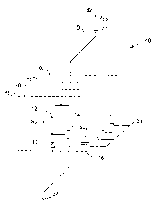
25 Referring to figure l, a basic prior art CMOS active pixel sensor (APS) 10
is
shown. This three transistor APS 10 is the simplest active sensor in the art.
The
photodiode 1 l, which is a light sensitive element, is pra-charged by a reset
transistor
12 under the control of a reset signal SR. This places the sensor node 11 at
the power
supply voltage Vpp. As light falls upon this diode 11, the sensor node 13 is
3o discharged. As the sensor nodel3 becomes increasingly discharged, the power
transistor 14 opens and the power becomes increasingly disconnected from the
output
node 15. When the output enable signal SoE is activated, the output transistor
16
becomes conductive, and the amplitude of the charge placed on the column line
17 is
dependent on the continuity between the power supply VDD and output node 15,
35 which is dependent on the charge on node 13.
CA 02351025 2001-06-19
Figure 2 illustrates APS's 10 organized in a typical array 20, which lies in
the
focal plane of the transducer. The APS's 10 in array 20 are arranged in a
number N of
columns and a number M of rows, such that each column includes M APS's and
each
row includes N APS's.
5
Though arrays 20 would normally include hundreds of rows and columns of
APS's 10, figure 3 is being simplified for description purposes by
illustrating a
column 30 having four APS's 101, 10z, 103 and 104 which are essentially
identical.
Each of the APS's 101, 102, 103 and 104 include a photodiode 11, a reset
transistor 12,
1 o a power transistor 14 and an output transistor 16. The APS's 1 q, 102, 103
and 104
share a common column output 31 that in turn is connected to a column
amplifier.
The APS's 101, 102, 103 and 104 are supplied in parallel, between a power
supply 32
voltage VDn and a ground 33. In addition, each of the APS's 101, 10z, 103 and
104 are
reset in sequence by reset signals SR applied to reset transistors 12 and are
read out
t 5 sequentially by output enable signals SoE, applied to output transistors
16. Thus
whether the output signals on line 31 are used in the processing of the image
sensed
by the transducer array 20 or not, it can be seen that column 30 circuitry
consumes
power in the process.
20 In order to preserve power during decimation in accordance with the present
invention, power is cut off to columns that are decimated. Figure 4
illustrates a
column 40 in accordance with the present invention. Column 40 includes four
APS's
101, 102, 103 and 104, which are essentially identical. Each of the APS's 101,
10~,
103 and 104 include a photodiode 11, a reset transistor 12, a power transistor
14 and an
25 output transistor 16. The APS's 101, 102, 103 and 104 share a common column
output
31 that in turn is connected to a column amplifier. The APS's 10~, 10z, 103
and 104
are supplied in parallel, between a power supply 32 voltage VDO and a ground
33. In
addition, each of the APS's 101, IOZ, 103 and 104 are reset in sequence by
reset signals
SR applied to reset transistors 12 and are read out sequentially by output
enable
3o signals SoE, applied to output transistors 16. However, in this particular
embodiment,
a power enable transistor 41 is connected in series with the four APS's 101,
102, 103
and 104 between power 32 and ground 33. In figure 4, the transistor 41 is
shown
connected between power terminal 32 and the APS's 101, 102, 103 and 104,
however,
transistor 41 could equally be connected between the APS's 101, 102, 103 and
104 and
CA 02351025 2001-06-19
6
ground terminal 33. Transistor 41 is responsive to a power enable signal SPE.
When
the output signals from a particular column 40 are to be used in the
processing of the
image sensed by the transducer array 20, a high power enable signal SPEis
applied to
the transistor 41 energizing the four APS's 10,, 102, 103 and 104. When the
output
signals from a particular column 40 are not to be used in the processing of
the image
sensed by the transducer array 20, a low power enable signal SPE is applied to
the
transistor 41, and the four APS's 101, 102, 103 and 104 remain de-energized
preventing
power consumption by the particular column 40 and therefore preserving power
consumption in the transducer array 20.
Though in the above embodiment the power enable transistor 41 is described
as being connected in series with a column 40 of APS's 101, 10~, 103 and 104
between
power terminal 32 and ground terminal 33, a row of APS's may equally be
controlled
in the same manner by connecting a power enable transistor in series with a
row of
t 5 APS's between a power terminal and ground terminal. Therefore, all further
description regarding column power control is equally applicable to row power
control.
Figure 5 schematically illustrates an array 50 of N columns in accordance with
2o the present invention wherein it is desired to individually control the
power to each of
the columns 401 to 40N so that the columns that are decimated are also de-
energized.
In this particular embodiment, every column 401 to 40N has one power cutoff
transistor 411 to 41N respectively that controls the power to all of the APS's
10 in that
particular column 401 to 40N. Power enable signals SPE are applied to the
gates of
25 power cutoff transistor 411 to 41N. A controller will generate the required
power
enable signals SPE depending on the number and type of decimation options that
are to
be provided by the transducer array 20. For simplicity of description only the
first
column 401, the last column 40N and a set of 8 sequential columns 40~+1 to
40"+s are
illustrated.
The columns 401 to 40N in the transducer array 50 may be controlled for
decimation in any of a variety of ways, such as by every 2°d 3'd, 4'h,
5'h, 6'h, 7th, 8th,
CA 02351025 2001-06-19
7
9'h, .......column, or even by halves, thirds, fourths, fifths, sixths,
sevenths, Bights,
ninths, . . . . ... of each column. By way of example, an embodiment of the
control of a
transducer array 50 will be described in conjunction with figure 5 wherein the
transducer array 50 is controlled such that it will allow for decimation by a
factor of 1
where no decimation takes place and all columns are energized, for decimation
by a
factor of 2 where every second column is energized, for decimation by a factor
of 4
where every fourth column is energized, and for decimation by a factor of 8
where
every eighth column is energized. In this particular embodiment the number of
columns N in the transducer array 50 is preferably an integer multiple of 8.
l0
Table 1 shows the state of any set of any 8 sequential columns where the first
column of the set is the (8*n+1)th column.
Column 8*n+18*n+28*n+3 8*n+48*n+5 8*n+68*n+78*n+g
DecimationCode A B C B D B C B
Factor (xy)
1 00 ON ON ON ON ON ON ON ON
2 O1 ON OFF ON OFF ON OFF ON OFF
4 10 ON OFF OFF OFF ON OFF OFF OFF
I 8 I 11 ON OFF OFF OFF OFF OFF OFF OFF
I I I
Table 1
In table 1, the state, ON or OFF, of the transistors for the column 40n+i to
40"+g
2o respectively are shown for the four decimation modes illustrated. The first
column
40n+i of the set is ON in every one of the four modes. The 2"a 4th, 6th, and
8th columns,
40~+2~ 40n+4~ 40n+6 and 40"+s respectively are only ON during mode 1 which is
the
non-decimation mode. The 3'd and 7'h columns 40"+3 and 40~+~ respectively is
ON in
decimation modes 1 and 2, and the 5'h column 40n+s is ON in modes l, 2, and 3.
Using a two digit binary code, as shown on table 1, to implement the
decimation factor in an IC, figure 6 illustrates circuits 60 that will
properly generate
the power enable signals SPE associated with each of the decimation factors.
Circuits
60 include an or-gate 61, an inverter 62 and an ancpgate 63. These signals
SpEA, SPEB,
CA 02351025 2001-06-19
g
SPEC, and SPED are applied to specific column power cutoff transistors 41 "+1
to 41 "~ as
shown in table 1. Since columns 40~+~ are always ON, the SpEASignal can be
tied
high, or associated transistors 41"+~ may be omitted. SpEBis applied to
columns 40~+z~
40"+a~ 40"+6 and 40"+s, SPEC is applied to columns 40"+3 and 40n+7 and SPED is
applied
to columns 40~+s.
As described above, the control of power consumption by an APS
transducer array may also be achieved by controlling rows of APS's. However,
in
addition, control may also be achieved by controlling both columns and rows
to simultaneously as exemplified by figure 7 that illustrates a small portion
of an APS
transducer array 70. A portion of a column 40N includes four APS's 101, l Oz,
103 and
104, which each include a photodiode 11, a reset transistor 12, a power
transistor 14
and an output transistor 16. The APS's 101, 10z, 103 and 104 share a common
column
output 31 that in turn is connected to a column amplifier. The APS's lOb 10z,
103,
104 .. . . .. are supplied in parallel, between a power supply 32 voltage VDD
and a
ground 33. A power enable transistor 41N is connected between power terminal
32
and the APS's 101, 10z, 103, 104...... Transistor 41N is responsive to a power
enable
column signal SpEN. In addition each of the APS's 101, l Oz, 103, 104. . . . .
. are
connected to a ground line each ground line being common to all of the APS's
in a
particular row. Each of the ground line 72,, 72z, 723, 724, . .. . . . are
then connected to
ground 33 through power enable transistors 711, 71z, 713, 714, ......
respectively,
which are responsive to power enable row signals SpERI, SpERZ, SPER,
SpER4..... .
When the output signals from the APS's in all of the columns and the rows are
to be
used in the processing of the image sensed by the transducer array 70, a high
power
enable signal SpEN is applied to the transistor 41N and further high power
enable
SlgnalS SpERI~ SpER2, SpER, SpER4~ ~ ~~. are applied t0 transistors 71 ~, 71z,
713, 714, ......
energizing the APS's 101, 10z, 103, 104.... When the output signals from a
particular
column 40N and particular rows are not to be used in the processing of the
image
sensed by the transducer array 70, a low power enable signal SpEN is applied
to the
3o transistor 41 and/or a low power enable signal SpERI, SpERZ, SpER,
SpER4..... is applied
to one or more of transistors 71,, 71z, 713, 714, ......, and either the APS's
101, 10z,
103, 104 ..... remain de-energized or selected APS's 101, 10z, 103, 104 .....
remain de-
CA 02351025 2001-06-19
energized, preventing power consumption by the particular APS's and therefore
preserving power consumption in the transducer array 20. Using the above
method,
allows for power savings when using versatile and sophisticated decimation
patterns.
While the invention has been described according to what is presently
considered to be the most practical and preferred embodiments, it must be
understood
that the invention is not limited to the disclosed embodiments. Those
ordinarily
skilled in the art will understand that various modifications and equivalent
structures
and functions may be made without departing from the spirit and scope of the
to invention as defined in the claims. Therefore, the invention as defined in
the claims
must be accorded the broadest possible interpretation so as to encompass all
such
modifications and equivalent structures and functions..