Note: Descriptions are shown in the official language in which they were submitted.
CA 02351037 2001-06-19
-1
Goren-Jin-Kochanski-Zhu 1-195-54-54
IV~Tf',ItOWAVE VACUUM TUBE DEVICE EMPLOYING GRID
MODULATED COLD CATHODE SOURCE HAVING NANOTUBE
EMITTERS
BACKGROUND OF THE INVENTION
Field of the Invention
The invention relates to microwave vacuum tube devices, in
particular tubes modulated by a proximately positioned grid
structure, i.e. gridded tubes.
1o Discussion of the Related Art
Microwave vacuum tube devices, such as power amplifiers, are
essential components of many modern microwave systems including
telecommunications, radar, electronic warfare and navigation
systems. While semiconductor microwave amplifiers are available,
~5 they generally lack the power capabilities required by most
microwave systems. Microwave vacuum tube amplifiers, in contrast,
can provide higher microwave power by orders of magnitude. The
higher power levels of vacuum tube devices are the result of the fact
that electrons can travel at a much higher velocity in a vacuum with
2o much less energy losses than in a solid semiconductor material. The
higher speed of electrons permits a use of the larger structure with
the same transit time. A larger structure, in turn, permits a greater
power output, often required for efFicient operations.
Microwave tube devices typically operate by introducing a
25 beam of electrons into a region where the beam interacts with an
input signal, and deriving an output signal from the thus-modulated
beam. See, e.g., A. S. Gilmour, Jr., Microwave Tubes, Artech House,
1986, 191-313. Microwave tube devices include gridded tubes (e.g.,
triodes, tetrodes, and klystrodes), klystrons, traveling wave tubes,
3o crossed-field amplifiers and gyrotrons. All require a source of emitted
CA 02351037 2001-06-19
-2-
Goren-Jin-Kochanski-Zhu 1-195-54-54
electrons. For example, a conventional klystrode 10 is shown in Fig.
1. The klystrode contains 5 main elements - a cathode 12, a grid 14,
an anode 16, a tail pipe 18, and a collector 20. The whole tube is
optionally placed in a uniform magnetic field for beam control. In
operation, a RF voltage is applied between the cathode 12 and grid
14 by one of several possible circuit arrangements. For example, it
is possible for the cathode to be capacitively coupled to the grid or
inductively coupled with a coupling loop into an RF cavity containing
the grid structure. The grid 14 regulates the potential profile in the
io region adjacent the cathode, and is thereby able to control the
emission from the cathode.
The resulting density-modulated (bunched) electron beam 22
is accelerated toward the apertured anode 16 at a high potential.
The beam 22 passes by a gap 19, called the output gap, in the
i5 resonant RF cavity and induces an oscillating voltage and current in
the cavity. RF power is coupled from the cavity by an appropriate
technique, such as inserting a coupling loop into the RF field within
the cavity. Finally, most of the beam passes through the tail pipe 18
into the collector 20. By depressing the potential of the collector 20,
2o some of the do beam power can be recovered to enhance the
efficiency of the device. Demonstrated efficiency of such devices is
relatively high, e.g., reaching 50% at 1 GHz, and the typical gain is
about 25 dB at 1 GHz.
The usual source of electrons for such microwave tube devices
2s is a thermionic emission cathode, which is typically formed from
tungsten that is either coated with barium or barium oxide, or mixed
with thorium oxide. Thermionic emission cathodes must be heated
to temperatures around 1000°C to produce sufficient thermionic
electron emission current, e.g., on the order of amperes per square
CA 02351037 2001-06-19
-3-
Goren-Jin-Kochanski-Zhu 1-195-54-54
centimeter. (As used herein, thermionic cathode indicates a cathode
that must be heated to at least 800°C to provide measurable
emission.) The necessity of heating thermionic cathodes to such
high temperatures creates several problems. For example, the
s heating limits the Lifetime of the cathodes, introduces warm-up
delays, requires bulky auxiliary equipment for cooling, and tends to
interfere with modulation of emission in gridded tubes. The limited
lifetime is due to the fact that the high operating temperatures cause
constituents of the cathode, such as the barium or barium oxide, to
io evaporate from the hot surface. It is possible for the evaporated
barium or barium oxide to then deposit onto the grid, which causes
undesirable grid emission that essentially renders the device
ineffective. Moreover, once the barium is depleted from the cathode,
the cathode (and hence the tube) no longer functions. Many
~5 thermionic vacuum tubes therefore have operating lives of less than
a year. The delay in emission is due to the time required for
temperature ramp-up, and delays as long as four minutes are not
uncommon. Such delays are unacceptable for many applications.
For gridded tubes, such as the klystrode 10 of Fig. 1, the high
2o temperature environment near the grid electrode tends to introduce
thermally induced geometrical and/or dimensional instability that
changes the cathode-grid spacing, e.g., due to thermal expansion
mismatch or structural sagging. These changes to the spacing tend
to significantly interfere with the ability of the grid to modulate the
25 cathode emission, and thus interfere with the overall operation of the
gridded tube. Moreover, there is a certain minimum cathode-grid
spacing that must be maintained, to ensure that such dimensional
changes do not result in contact between the cathode and grid.
Because of this minimum spacing requirement, it is not possible to
CA 02351037 2001-06-19
-4-
Goren-Jin-Kochanski-Zhu 1-195-54-54
move the cathode and grid closer together in order to decrease the
cathode-grid transit time, which would in turn increase the
maximum operating frequency of the device. For this reason, the
frequency of gridded tubes with thermionic cathodes is limited.
s Thus, there is a need for an improved electron source for
microwave tube devices, particularly gridded tubes, which avoids
problems of conventional devices and is able to reduce transit times.
SUMMARY OF THE INVENTION
The invention relates to an improved gridded-type microwave
io tube, in which a cold cathode containing carbon nanotube emitters
is used. Use of the cold cathode avoids the problems encountered
with thermionic cathodes, and allows the grid and cathode spacing
to be substantially reduced, thereby reducing transit time of the
electrons. In fact, a microwave tube of the invention generally
~s exhibits a transit time at least 2x shorter than a similar tube having
a thermionic cathode. And the operating frequency of a microwave
tube of the invention is generally enhanced at least 2x compared to a
similar tube having a thermionic cathode.
The gridded tube of the invention contains a cold cathode, an
2o anode, and a grid located between the anode and cathode, such as
shown by the conventional klystrode of Fig. 1. In one embodiment,
the cold cathode has a refractory metal substrate and carbon
nanotube emitters. The nanotube emitters have a diameter of 1 to
300 nm and a length of 0.05 to 100 ~m (length indicating the actual
25 length of the nanotubes regardless of their geometrical
configuration). Advantageously, the height of the nanotubes from
the cathode substrate is relatively uniform, e.g., at least 90% of the
CA 02351037 2001-06-19
-s-
Goren-Jin-Kochanski-Zhu 1-195-54-54
nanotubes have a height within about 20% of the average height.
The grid-cathode spacing is 1 to 100 ~,m, the grid contains apertures
having a maximum dimension of 0.1 to 100 Vim, and the grid
thickness is 0.1 to 50 Vim. Emission from the cathode directly onto
s the grid material itself, which undesirably heats the grid, is reduced
by either (a) the presence of a shadow mask on the emitters or (b)
selective formation of the emitters in locations that correspond to the
grid apertures. The microwave tube operates at a frequency of
greater than 0.5 GHz, advantageously greater than 2 GHz.
io
BRIEF DESCRIPTION OF THE DRAWINGS
Fig. 1 illustrates a conventional klystrode type of microwave
tube.
Figs. 2A to 2C illustrate cold cathode and grid configurations
~ s according to aspects of the invention.
Figs. 3A and 3B illustrate cold cathode designs according to
other aspects of the invention.
Figs. 4A and 4B illustrate technique for forming emitter
structures according to further aspects of the invention.
2o Fig. 5 shows the operation of a triode microwave vacuum tube
configuration according to the invention.
DETAILED DESCRIPTION OF THE INVENTION
The invention provides an improved gridded microwave tube
2s that uses a cold cathode having carbon nanotube emitters. The cold
cathodes are capable of fast, nearly instantaneous, room
temperature emission when an electric field is applied. The cold
cathode allows the grid to be positioned very close to the cathode,
providing direct modulation of the electron beam signals (by the grid)
CA 02351037 2001-06-19
-6-
Goren-Jin-Kochanski-Zhu 1-195-54-54
with substantially reduced transit time. The transit time in the
inventive device is generally shortened by a factor of at least 2
compared with a similar tube structure containing a thermionic
cathode. The operating frequency of the inventive microwave tube is
s also typically enhanced by a factor of at least 2 compared with a
similar tube structure containing a thermionic cathode. In
particular, the cathode-grid gap in the inventive tube device is
relatively small, typically 1 to 100 Vim, advantageously 1 to 20 ~,m,
whereas gaps in gridded tubes containing thermionic cathodes
io generally are greater than 100 ~.m.
Carbon nanotubes are attractive as field emitters because their
high aspect ratio (>1,000), one-dimensional structure, and small tip
radii of curvature (~ 10 nm) tend to effectively concentrate the electric
field. In addition, the atomic arrangement in a nanotube structure
i5 imparts superior mechanical strength and chemical stability, both of
which make nanotube field emitters robust and stable. It is possible
to prepare carbon nanotubes by a variety of techniques, including
carbon-arc discharge, chemical vapor deposition via catalytic
pyrolysis of hydrocarbons, laser ablation of a catalytic metal-
2o containing graphite target, or condensed-phase electrolysis.
Depending on the method of preparation and the specific process
parameters, the helicity and the diameter of the tubules, the
nanotubes can be produced mufti-walled, single-walled, or as
bundles of single-walled tubules, and can adopt various shapes such
25 as straight, curved, planar-spiral and helix. Carbon nanotubes are
typically grown in the form of randomly oriented, needle-like or
spaghetti-like powders. However, oriented nanotube structures are
also possible, as reflected in Ren et al., Science, Vol. 282, 1105,
(1998); Fan et al., Science, Vol. 283, 512 (1999).
CA 02351037 2003-05-08
_7_
Carbon nanotube emitters are discussed, for example, in Rinzler et
al. , Science, Vol. 269, 1550 (1995); De Heer et al. , Science, Vol. 270,
1179 (1995); Saito et al., Jpn. J. Appl. Phys., Vol. 37, L346 (1998); Wang
et al., Appl. Phys. Lett., Vol. 70, 3308, (1997); Saito et al., Jpn. J. Appl.
Phys., Vol. 36, L1340 (1997); Wang et al., Appl. Phys. Lett., Vol. 72,
2912 (1998); and Bonard et al., Appl. Phys. Lett., Vol. 73, 918 (1998).
Techniques for forming nanotube field emitter structures, with both oriented
and non-oriented nanotubes structures are also described in U.S. Patents
such as No. 6,250,984 issued June 26, 2001, No. 6,283,812 issued
January 25, 1999 and No. 6,277,318 issued August 18, 1999.
As reflected in these techniques, it is possible to form carbon
nanotube emitters on substrate by either in-situ growth or post-deposition
spraying techniques. For in-situ growth, the substrate is generally placed in
a chemical vapor deposition chamber, and pre-coated with a thin layer (e.g.,
1-20 nm thick) of catalyst metal such as Co, Ni or Fe (or formed from such
a metal) . The gas chemistry is typically hydrocarbon or carbon dioxide
mixed with hydrogen or ammonia. Depending on specific process
conditions, it is possible to grow the nanotubes in either an aligned or
random manner. Optionally, a plasma assisted chemical vapor deposition
technique is used to grow highly aligned nanotubes on the substrate surface,
as disclosed in co-assigned U.S. Patent No. 6,277,318 issued
August 18, 1999. For non-flat cathode surfaces, such a plasma assisted
CVD technique is particularly useful for growing conformally-aligned
nanotubes. Other techniques are also possible.
In a typical post-deposition technique, pre-formed and
CA 02351037 2001-06-19
-8_
Goren-Jin-Kochanski-Zhu 1-195-54-54
purified nanotube powders are mixed with solvents and optionally
binders (which are pyrolized later) to form a solution or slurry. The
mixture is then disposed, e.g., screen printed or dispersed by spray,
spin-on, or electrophoresis, onto a substrate, the substrate
s optionally containing carbon dissolving elements (e.g., Ni, Fe, Co) or
carbide forming elements (e.g., Si, Mo, Ti, Ta, Cr), to form a desired
emitter structure. Annealing in either air, vacuum or inert
atmosphere is followed to drive out the solvent, leaving a nanotube
emitter structure on the substrate. And where the carbon dissolving
or carbide forming elements are present, annealing promotes
improved adhesion. Other post-deposition techniques are also
possible.
The diameter of the field-emitting nanotubes is 1 to 300 mm,
advantageously 1 to 100 mm. The length of the nanotubes is 0.05 to
i5 100 Vim, advantageously 0.5 to 20 ~.m. To maintain the small gap
between the cathode and the grid, and thereby achieve a reduced
transit time and a higher operating frequency, the nanotubes
advantageously exhibit a relatively uniform height, e.g., at least 90%
of the nanotubes have a height that varies no more than 20% from
2o the average height.
Because of the manometer scale of the nanotubes, the
nanotube emitters provide many potential emitting points, typically
more than 109 emitting tips per square centimeter assuming a 10%
area coverage and 10% activated emitters from 30 mm (in diameter)
25 sized nanotubes. The emitter site density in the invention is typically
at least 103/cm2, advantageously at least 104/cm2 and more
advantageously at least 105/cm2. The nanotube-containing cathode
requires a turn-on field of less than 2 V/~m to generate 1 nA of
emission current, and exhibits an emission current density of at
CA 02351037 2001-06-19
-9-
Goren-Jin-Kochanski-Zhu 1-195-54-54
least 0.1 A/cm2, advantageously at least 0.5 A/cm2, at an electric
field of 5 to 50 V/~m.
It is desirable to have a gate structure with as many gate
apertures as possible, both for maximum emission efficiency and to
s minimize the heating effect caused by electrons intercepted by the
gate grids. The grid in the microwave tube of the invention is made
of a conductive metal, and has a perforated, mesh, or apertured
structure that draw the emitted electrons yet let the electrons pass
to the anode. An apertured grid structure is particularly useful.
io Such an apertured grid structure is prepared by photolithography or
other known patterning techniques. The apertures have an average
maximum dimension of 0.5 to 100 ~,m, advantageously 1 to 100 Vim,
more advantageously 1 to 20 Vim, and are able to be formed in a
variety of shapes. (Maximum dimension indicates the largest
is distance across the aperture, e.g., diameter for a circular aperture.)
In the case of a fine wire mesh screen, the wire diameter is typically
to 50 ~,m and the average maximum dimension is similarly 0.5 to
100 Vim, advantageously 1 to 100 Vim, more advantageously 1 to 20
Vim.
2o The grid is typically separated from the cathode either by
suspending the grid in the device or by placing one or more
electrically insulating spacers, e.g., Al2Os, between the grid and
cathode. The dimensional stability of the grid, particularly
maintenance of the gap between the cathode and the grid, is
2s important, as noted above. The grid is typically formed from a
mechanically strong, high melting point (at least 1600°C), low
thermal expansion metal such as a refractory or transition metal,
e.g., Mo, W, Ta, Hf, Ni, or Cr. The use of relatively strong and creep-
resistant ceramic materials such as highly conductive oxides,
CA 02351037 2001-06-19
-lo-
Goren-Jin-Kochanski-Zhu 1-195-54-54
nitrides, and carbides is also possible (conductive or conductor
indicating a material having an electrical resistivity less than 5000
X52-cm). The grid is desirably configured to have as much
mechanical rigidity as possible. The typical thickness of the grid
s conductor, i.e., when an apertured grid is used, is 0.1 to 50 Vim,
typically 2 to 50 Vim.
In one embodiment, assembly of the grid to the cathode
structure uses only two parts. The first part is an insulating ring (or
three or more insulating pads) that is secured directly onto the
to emitters or onto the cathode substrate. The insulating ring is
formed from any suitable electrically insulating material, e.g.,
ceramics. They are advantageously of sufficient thickness such that
surface breakdown is prevented - typically offering greater than
3x 10⁻⁵ cm/volt (as measured along the surface from the cathode to
is the grid). The thickness of the insulating ring is able to be reduced if
the rings' upper and/or lower surface is properly textured. For
example, grooves or bumps on the ring surface will lengthen the
surface breakdown path, thereby increasing the breakdown voltage
and/or allowing reduced ring widths.
2o The second part of the assembly is a metal support ring to
which the periphery of the grid is attached, e.g., welded. The metal
ring is secured directly onto the insulating ring or spacers. The
metal support ring supports the grid, and also protects the upper
surface of the insulating ring from accidental deposition of
2s conductive material, e.g., from deposition of nanotubes in an
embodiment in which the emitters are formed after the grid is
secured to the cathode. The support ring is typically a metal such as
molybdenum or stainless steel, but it is also possible to use ceramic
rings. Such ceramic rings tend to allow tighter machining
CA 02351037 2001-06-19
-11-
Goren-Jin-Kochanski-Zhu 1-195-54-54
tolerances, and also will be more likely to have thermal expansion
coefficients more closely matched to the insulating pad.
Additionally, ceramics allow a longer insulating path over which it is
possible to drop the emitter-grid voltage.
Excessive heating of the grid structure due to impacts of
electrons will tend to induce expansion and sagging of the grid,
which will in turn change the spacing between the cathode and grid,
the electric field, and thus the emission characteristics. Moreover,
when a grid is substantially expanded due to thermal effects, it is
io possible that a portion of the grid will even touch the cathode,
causing an electric short and catastrophic failure of the entire
device. To reduce such grid heating, the gridded tube of the
invention uses either a shadow grid directly placed on the cathode
surface or selective formation of the emitters on the cathode surface.
~5 The shadow grid is identical to the structure of the active grid, and
covers or blocks the emitters directly underneath the active grid
material, thereby preventing emitting electrons from impacting the
grid. One technique for forming the shadow grid is to align, place
and optionally bond a structure identical to the active grid onto the
2o nanotube cathode surface.
Selective formation of the nanotube emitters is performed by
any suitable technique. One technique is to spray a pre-formed
nanotube suspension through a grid structure onto the substrate,
such that the resulting cathode will have emitters formed primarily
2s under the grid apertures. Another technique is to deposit a catalyst
metal for nanotube formation in a pattern corresponding to the grid
apertures, e.g., by sputter-deposition through a shadow mask.
Nanotubes are then formed on the patterned catalyst metal by a
chemical vapor deposition process, as discussed above.
CA 02351037 2001-06-19
-12-
Goren-Jin-Kochanski-Zhu 1-195-54-54
The carbon nanotubes are generally attached or formed on the
surface of the cathode substrate before the grid structure is
assembled. The cathode substrate typically contains an electrical
conductor such as a metal, doped semiconductor, or conductive
s oxide, carbide, or nitride (conductor or conductive has the same
meaning indicated above). Advantageously, particularly for high
current operation, the substrate contains a refractory metal with a
high melting temperature (i.e., at least 1600°C), e.g., W, Mo, Ta, Hf,
or Zr. It is possible for the surface of the cathode substrate to be
io flat, or curved (e.g., concave), as discussed in more detail below.
Fig. 2A illustrates a cathode and grid structure according to
one embodiment of the invention. The surface of the cathode
substrate 30 contains a pre-coated layer 31 of a carbon dissolving or
carbide forming element, e.g., sputtering or electrochemically plating
is a thin iron layer. (As used herein, cathode substrate includes a
substrate and any layers formed thereon.) Pre-formed nanotubes 32
are then spray coated on the substrate, typically in a suspension,
and the structure is then heat treated to induce diffusional reaction
of nanotubes with iron to promote bonding of the nanotubes to the
2o substrate 30. A shadow grid 33 is placed directly on the nanotubes
32 to block the emission from under the shadow grid and thereby
reduce unwanted electron bombardment of the grid. The grid 34 is
then aligned with the shadow grid and fixed in position.
Another embodiment of a cathode and grid structure is
2s illustrated in Fig. 2B. In this embodiment, the cathode substrate 40
contains a patterned catalyst material 41, and the nanotubes are
grown directly on the catalyst material 41 by a CVD process. The
catalyst material 41 is patterned to correspond to the apertures of
the grid 43. Advantageously, a microwave or RF plasma enhanced
CA 02351037 2001-06-19
-13-
Goren-Jin-Kochanski-Zhu 1-195-54-54
CVD process, as discussed above, is used to provide aligned carbon
nanotubes 42.
In CVD fabrication of nanotubes, it is possible to encounter
some difficulty in forming nanotubes on a refractory metal substrate
s having a catalyst metal thereon. As reflected in Fig. 2C, for a
refractory metal substrate 50, it is therefore advantageous to form a
layer of silicon 51, e.g., a 1 to 100 nm thick layer formed by
sputtering or evaporation, on the refractory metal substrate 50. The
catalyst material 52 is then formed on the silicon, and the CVD
to nucleation and growth of nanotubes 53 is performed. The grid 54 is
then provided.
The silicon layer appears to provide anchoring points for the
growing nanotubes by creating a silicide of the catalyst material. To
further improve the adhesion of the silicon layer to the refractory
is substrate, it is possible to provide an alloy containing both silicon
and the refractory metal. Instead of forming such an alloy layer, it is
also possible to deposit a layer having a composition gradient, such
as by using a two-target sputtering approach and initially making
the layer rich in the refractory metal (e.g., at least 70 wt.%) with a
2o gradual transition to a silicon-refractory metal mixture and then to a
silicon-rich composition (e.g., at least 70% in weight).
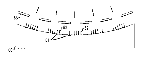
Figs. 3A and 3B illustrate embodiments using curved cathode
surfaces, which generally provide improved focusing of the electron
beam in a gridded microwave tube. (The designs reflected in Figs. 2A
25 to 2C are applicable to such curved surfaces.) In the embodiment of
Fig. 3A, a cathode substrate 60 having a curved surface is provided
and contains patterned regions of a catalyst material 61. Nanotubes
62, advantageously aligned, are formed on the catalyst by a CVD
technique, and a grid structure 63 is then provided. In the
CA 02351037 2001-06-19
-14-
Goren-Jin-Kochanski-Zhu 1-195-54-54
embodiment of Fig. 3B, a refractory metal cathode substrate 70 with
a curved surface is provided, and contains a silicon layer 71.
Regions of a catalyst material 72 are patterned on the silicon layer
71, and nanotubes 73, advantageously aligned nanotubes, are
s formed by a CVD technique on the catalyst material. A grid 74 is
then provided, with the apertures arranged over the selectively
formed nanotube emitters.
A slightly concavity of the cathode away from the grid is also
able to compensate for some sagging of the grid. Specifically, the
o grid will tend to sag under the influence of electrostatic forces as
voltage is applied between the grid and the cathode. It is possible,
as noted above, for such sagging to contribute to damage or
destruction of the tube. In addition, for a flat cathode surface, the
electric field under the center of the grid will increase as the grid
is sags, because the same voltage is dropped across a smaller distance.
This increased electric field will cause the field emitters under that
portion of the grid to emit far more strongly than the emitters around
the edge, resulting in a non-uniform emission. The concavity of the
cathode is advantageously selected, therefore, to self consistently
2o match the grid shape at the operating voltage.
It is also possible to use a tensioned grid. The grid is attached
to a support ring, as discussed above, such that the grid will be
under tension at its normal operating temperature. This tension
will tend to keep the grid flatter and will also inhibit sagging.
2s Excessive variation of the height of the nanotubes tends to
cause some variation in the gap between the cathode emitting tips
and the grid, and leads to undesired fluctuations in the local electric
field. It is possible for any particularly long nanotubes to actually
touch the grid and thereby cause an electrical short and failure of
CA 02351037 2003-05-08
-15-
the device. Advantageously, the growth conditions are controlled to provide
a relatively uniform height of the nanotubes, e.g., as in the plasma enhanced
CVD technique noted above. In cases where the variation is greater than
desired, however, it is possible to provide improved uniformity. One
technique for providing more uniform nanotubes uses a high-energy beam
such as a laser beam, an electron beam, an ion beam, or a gas plasma beam.
(See U.S. Patent No. 6,283,812). It is possible to use a point source beam,
a multiplicity of parallel beams, or a planar beam, either in a stationary
mode or in a scanning mode of illumination. As reflected in Fig. 4A, the
portions of carbon nanotubes 82 contacted by the beam 83 are evaporated,
and the nanotubes 82 are truncated one after another as the beam 83
propagates through the nanotubes. (The nanotubes are formed on a catalyst
layer 81 present in the substrate 80). A light vacuum suction or a gentle gas
blow is typically used either during or after the truncating process in order
to reduce the extent to which broken-off ends 84 are trapped in the
remaining nanotube structure. It is also possible to sweep the beam from
the upper ends of the nanotubes down to the desired height, such that the
undesired portions of the nanotubes are substantially evaporated, instead of
merely truncated. The beam energy depends on the nature of the beam, the
size and density of nanotubes, and the mode of beam operation. For
example, in the case of an excimer laser (such as an ArF laser), the desired
energy is typically in the range of 0.1 -100 milli Joule per pulse with a
pulse duration of 1 - 100 nanoseconds, operated at 1 - 1.000 Hz repetition
rate.
Fig. 4B illustrates an alternative technique for truncating carbon
nanotubes, using oxygen and a temperature gradient.
CA 02351037 2001-06-19
-16-
Goren-Jin-Kochanski-Zhu 1-195-54-54
Substantially all forms of solid carbon burn in the presence of an
oxygen-containing atmosphere at high temperature. In the
technique reflected in Fig. 4B, the top portions of carbon nanotubes
92 (formed on a catalyst layer 91 of a substrate 90) are brought into
s contact with a hot blade 93 in an oxygen-containing atmosphere.
The hot blade provides a temperature gradient near the top portions
of the nanotubes, and those parts of the nanotube which reach a
critical temperature, e.g., about 400°C or higher, react with oxygen
and are removed. The critical temperature depends on the oxygen
io partial pressure in the atmosphere, the time of contact between the
hot blade and the carbon nanotubes, as well as the diameter of the
each nanotube (or each bundle of nanotubes). The hot blade is
formed from any suitable metallic or ceramic material, and is heated
by any suitable means. The desired temperature of the blade tip
is which contacts the nanotube is at least 400°C, preferably at least
600°C.
The invention will be further clarified by the following
example, which is intended to be exemplary.
Example 1
2o Single-wall carbon nanotubes produced by a laser ablation
technique were suspended in acetone in an ultrasonic bath. The
suspension was sprayed onto a molybdenum cathode surface having
a diameter of about 5.5 mm, on which had been sputtered an
approximately 1 ~m thick iron film. The cathode was then annealed
2s in vacuum ( 10-6 torr) at 800°C for one hour. The field emitter was
assembled in a triode configuration having a molybdenum grid
mechanically secured 125 ~m from a grounded nanotube field
emitter cathode. The grid was formed of a wire mesh screen with
about 25 ~m diameter wires and square-shaped aperture openings of
CA 02351037 2001-06-19
-17_
Goren-Jin-Kochanski-Zhu 1-195-54-54
about 75 ~,m. A 6 KV anode was placed at a location about 5 mm
from the grid. A voltage of 900V was applied to the grid, and the grid
was pulsed at 1 % duty with 80 microsecond long pulses. Fig. 5
illustrates the grid voltage trace as well as the electron beam
s currents that impinged on the anode. A total cathode current
density, including the anode current and the grid current (the grid
current is not shown in Fig. 5), of about 0.24 A/cm2 was observed.
Other embodiments of the invention will be apparent to those
skilled in the art from consideration of the specification and practice
io of the invention disclosed herein.