Note: Descriptions are shown in the official language in which they were submitted.
CA 02351201 2001-06-21
AN IMPROVED MOTOR DRIVER CIRCUIT
Field of the Invention
The present invention relates generally to a driver circuit and, more
particularly, to a motor driver adapted to provide selectable current levels
of
a drive current for driving a motor externally coupled to the motor driver.
Background of the Invention
A conventional motor driver, such as a chopper motor driver, is
generally designed to limit the amount of current that a motor can draw from
a power supply. As a result, the motor will not draw more current than
necessary for operation, thereby increasing the power efficiency of the motor
and the motor driver. More importantly, by limiting the current supplied to
the
motor, the conventional motor driver prevents too much current from flowing
through the motor than the motor could handle so that the motor will not burn
up.
A conventional arrangement of the motor driver 10 and the motor 30
is shown in Figure 1. The conventional motor driver 10 includes a driver
circuit 12 coupled to a reference circuit 14. The reference circuit 14
typically
includes a voltage divider 22 for generating a predetermined reference
voltage V, to the motor driver 10. Ordinarily, the voltage divider 22 has
first
R1 and second R2 resistors 24, 26 connected in series between power supply
V~ 32 and ground node 38. The reference voltage V, is defined as the
voltage at node 28, where the first R1 and second R2 resistors 24, 26 join.
As a result, the reference voltage V, is defined as
Vf = V~ x R2/(R1+R2)
where the V~ is a predetermined stable voltage. By selecting the first R1 and
second R2 resistors 24, 26, a user of the motor driver 10 can provide a fixed
-1-
CA 02351201 2001-06-21
reference voltage V, for determining how much current could flow through the
motor 30, as will be further explained in the following paragraphs.
The drive circuit 12 of the conventional motor driver 10 includes a
compare circuit 20, as shown in Figure 1. Normally, the node 28 is coupled
to one terminal 42 of the compare circuit 20 for receiving the reference
voltage V,. In addition, the other terminal 44 of the compare circuit 20
receives a sense voltage from an output 40 of a sense circuit 18. Therefore,
the compare circuit 20 compares the reference voltage V, with the sense
voltage VS to generate a compare voltage Vop at its output. As shown in
Figure 1, the compare circuit 20 often includes an op-amp 36 to compare the
reference voltage Vf with the sense voltage Vg for generating the compare
voltage Vop at the output of the op-amp 36 based on the relative difference of
the Vf and Vs.
As shown in Figure 1, the drive circuit 12 also includes the switch
circuit 16 coupled in series between the motor 30 and the sense circuit 18 of
the drive circuit 12. The sense circuit 18 generally includes a sense resistor
RS 34 coupled in series between the switch circuit 18 and the ground node 38.
As a result, a current I~ flowing through the motor 30 will also flow through
the
sense resistor R, 34 by way of the sense circuit 18.
Figure 1 shows the sense resistor Rs 34 being coupled to the compare
circuit 20 at the output node 40. Thus, the sense voltage VS, which is the
voltage at the output node 40, is defined as
Va = Ic X Rs
where the current I~ is the same current flowing through the motor 30, the
switch circuit 16, and the sense resistor R, 34.
As mentioned, the sense voltage Vs is fed into the other terminal 44 of
the comparator 36 to be compared with the reference voltage Vf fed into one
input terminal 42 of the op-amp 36. If the VS is larger than the V,, the
output
voltage VoP of the op-amp 36 will force the switch circuit 16 to open, i.e.,
to
-2-
CA 02351201 2001-06-21
stop conducting the current I~ from the motor 30. As a result, the motor 30
will
not draw any current from power supply Vp$ 46. Simultaneously, the sense
voltage Vs will start to drop since no current is now flowing through the
sense
resistor Rg 34 due to the open circuit of the switch circuit 16. After the
sense
voltage VS has dropped to a level lower than the reference voltage V,, the
output voltage Vop of the op-amp 36 will then cause the switch circuit 16 to
close, i.e., to start conducting the current I~ from the motor 30, and the
sense
voltage Vs will then start to rise. In short, the configuration of the
conventional
motor driver 10 provides a feedback loop between the drive circuit 12 and the
reference circuit 14, whereby a feedback voltage, i.e., the sense voltage Vs,
is compared to the reference voltage V, for determining the status (open or
close) of the switch circuit 16. Therefore, the sense voltage Vs will be
confined within a range approximately equal to the reference voltage V, and
the current flowing through the motor 30 will be defined approximately as
I~ = Vt / RS.
Comparing the sense voltage V, with the predetermined reference
voltage V, effectively allows the conventional motor driver 10 to control how
much current current I~ will flow through the motor 30. Therefore, the motor
30 will be protected from burning up due to the excessive heat generated by
the excessive current. Also, a specific torque characteristic can be achieved.
The conventional motor driver 10, however, has several disadvantages.
Generally, the motor 30 needs a relatively large current to start the
motor's rotor during an initial operating stage. In contrast, the motor 30
needs only a much lower current level to maintain rotation once it passes the
initial operating stage. For example, a larger initial torque ~; is needed to
overcome the static friction fs so as to initially start the motor 30 from
rest.
When the motor's rotor starts to rotate, a smaller torque f~ is required to
overcome a dynamic friction fd for maintaining rotation. The dynamic friction
Fd usually is smaller than the static friction fs. As a result, the initial
torque ~;
has to be larger than the rotating torque f~. Since only one reference voltage
V, is provided to the conventional motor driver 10, the reference voltage V,
has
-3-
CA 02351201 2001-06-21
to be set at a value that is sufficient to drive the motor 30 during the
initial
stage. As a result, the current I~, which is determined by the Vf, is defined
sufficiently large to drive the conventional motor 30 during the initial stage
but
is often larger than necessary after the motor 30 starts running.
Consequently, the conventional motor driver 10 consumes more electrical
power than necessary for operation and is less efficient.
Moreover, since a larger than necessary current I~ flows through the
motor 30, the motor driver 30 often generates excessive heat during
operation. The excessive heat will have an adverse effect on the reliability
of
the motor 30, or conventional motor driver 10. A heat sink may be added to
the conventional motor driver 10 to eliminate the excessive heat problem.
However, adding the heat sink will inevitably increase the complexity and
manufacturing costs and size of the conventional motor driver 10. An
improved motordriver solution is thus needed to resolve the above-mentioned
difficulties.
Summar~of the Invention
The present invention is directed to an improved motor driver circuit
having a select circuit for controlling a current level flowing through a
motor
coupled to the improved motor driver. In a preferred embodiment of the
present invention, the select circuit includes a DAC (Digital-to-Analog
Converter) for determining the current level of the motor. The DAC is coupled
to a drive circuit of the improved motor driver circuit to provide the drive
circuit
a reference voltage that is selectable from a plurality of voltage levels. The
drive circuit then, in response to the selected reference voltage supplied by
the DAC, controls the current level of the motor to its appropriate level
during
different stages of operation. In another embodiment, the present invention
further comprises a firmware program for controlling the DAC to output the
reference voltage. The firmware may be pre-programmed according to the
needs of the motor during various stages of operation.
-4-
CA 02351201 2001-06-21
The foregoing and other objects, features and advantages of the
invention will be apparent from the more particular description of preferred
embodiments of the invention, as illustrated in the accompanying drawings in
which like reference characters refer to the same parts throughout the
different views. The drawings are not necessarily to scale, emphasis instead
being placed upon illustrating the principles of the invention.
Brief Description of the Drawings
Figure 1 shows a conventional motor drive circuit coupled to a motor
and a power supply.
Figure 2 shows a preferred embodiment of an improved motor drive
circuit according to the present invention.
Detailed Description of the Invention
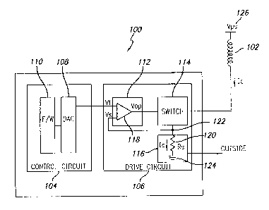
The present invention is directed to an improved motor drive circuit 100
which provides a selectable current level for a motor 102 during different
stages of motor operation. The motor 102 is coupled to the motor driver 100
and is not part of the present invention. The motor driver 100 includes a
control circuit 104 coupled to a first input of a drive circuit 106. In the
preferred embodiment, the control circuit 104 includes a DAC (Digital-to
Analog Converter) 108 having an output coupled to the first input of the drive
circuit 106. The output of the DAC 108 supplies a selectable reference
voltage Vf to be fed into the first input of the drive circuit 106.
The drive circuit 106 includes a compare circuit 112 coupled to a switch
circuit 114 at the output. The compare circuit 112 has a first and a second
input respectively coupled to the output of the DAC 108 through the first
input
of the drive circuit 106 and to a sense circuit 116, as shown in Figure 2. The
switch circuit 114 is coupled to the sense circuit 116 in series, whereby the
node 122 is positioned directly between the switch circuit 114 and the sense
circuit 116. Moreover, the switch circuit 114 is further coupled to the motor
102 in series, as shown in Figure 2.
-5-
CA 02351201 2001-06-21
The compare circuit 112 also has an output terminal coupled to the
switch circuit 114. Thus, an output voltage Vop of the op-amp 118 is provided
to the switch circuit 114 for controlling the status (open or close) of the
switch
circuit 114. For instance, when the output voltage Vop is at one level, the
switch circuit 114 will be closed (i.e., conducting) and is adapted to conduct
an electric current I~ flowing through the motor 102. When the output voltage
Vop is the opposite, the switch circuit 114 will be open and will not conduct
the
electric current I~ from the motor 102.
The sense circuit 116 defines a sense voltage VS at the node 122 to be
fed back to the comparator or op-amp 118. Basically, the sense circuit 116
uses a resistive load for determining the sense voltage VS at the node 122.
In the preferred embodiment, the sense circuit 116 includes a sense resistor
R$ coupled in series between the node 122 and the ground node 124, as
shown in Figure 2, so that the I~ will flow from the switch circuit 114
through
the sense resistor Rs into the ground node 124. The sense voltage VS at the
node 122 is, therefore, defined as
Vs=I~XRs
where I~ is the electric current flowing through the motor 102 and the sense
resistor RS and the Ra is the resistance of the sense resistor RS. In an
alternative embodiment, the sense resistor Rg may be replaced by a load
circuit or by other electrical components adapted to provide the suitable
means for determining the sense voltage Vs.
As mentioned, the output of the DAC 108 generates the selectable
reference voltage V, which is fed into the compare circuit 112, as shown in
Figure 2. The reference voltage V, functions to control the switch circuit 114
for determining the current level of the I~ flowing through the motor 102.
Moreover, when the Vop is at one level, the switch circuit 114 will be closed
to
conduct the I~ from the motor 102. When the Vop is at the other level, the
switch circuit 114 will open to disconnect the sense circuit 116 from the
motor
102. Therefore, the sense voltage Vg will start to drop due to the decreasing
-6-
CA 02351201 2001-06-21
current flow of I~. Once the sense voltage V$ has dropped to a level lower
than the reference voltage Vf, the VoP of the op-amp 118 will switch to the
first
level again and the switch circuit 114 will start conducting the I~ and start
raising the sense voltage Vg. By providing this dynamic feedback loop of the
drive circuit 106, the present invention can, thus, control the I~ in the
motor
102 approximately at a level corresponding to a selected voltage level of the
reference voltage V,.
As noted, the reference voltage V, provided by the DAC 108 is
selectable, i.e., the DAC 108 may choose the voltage level of the reference
voltage V, within a predetermined range. The voltage range of the V, should
be sufficiently large to provide enough voltage for rotating the motor rotor
during an initial operation stage of the motor 102. Moreover, the reference
voltage Vf should provide sufficient sustaining voltage for continuing to
rotate
the motor rotor after the initial operation state. The DAC 108 works to
convert
pre-selected digital bit information into analog voltage levels for outputing
the
reference voltage Vt. In the preferred embodiment, the DAC 108 has an
eight-bit configuration. As a result, the DAC 108 is capable of providing 256
voltage levels for the reference voltage Vf. In other alternative embodiments,
the DAC may have any suitable numbers of digital bit configuration adapted
for various applications.
In the preferred embodiment, the control circuit 104 of the present
invention further comprises a firmware 110 coupled to the DAC 108 for
controlling the same. The firmware 110 is pre-programmed to generate digital
bit information, 8 bits in the case of the preferred embodiment, according to
the operation stage of the motor 102. The digital bit information of the
firmware 110 is then fed into the DAC 108 for generating reference voltage
V, corresponding to the digital bit information.
By having the firmware 110 and the DAC 108 of the control circuit 104,
the present invention is adapted to provide different voltage levels of the
reference voltage V, to provide adequate current levels of the motor 102
during different stages of the motor operation. For example, during the
initial
CA 02351201 2001-06-21
operation stage, the reference voltage V, is set to a high value in order to
allow sufficiently large I~ in the motor 102 to provide a large initial torque
f; for
rotating the motor rotor. Once the motor 102 starts rotating, the firmware 110
causes the DAC 108 to generate a lower reference voltage V,, and thus lower
Ic, sufficient to maintain rotation of the motor 102. Because the motor 102
runs on a higher I~ only during the short period of the initial operation
stage,
the present invention has a better power efficiency as compared the
conventional motor driver. Moreover, since the DAC 108 has an 8-bit
configuration to provide 256 levels of reference voltage V,, the present
invention may dynamically adjust the reference voltage V, according to
various stages of the motor operation. This may further save substantial
power consumption, and improve power efficiency, of the motor driver 100.
As a result, the present invention needs no heat sink to dissipate heat
generated by the motor 102, as many conventional motor drivers do to
prevent thermal damages of the motor and/or the motor driver.
From the foregoing, it will be appreciated that, although specific
embodiments of the invention have been described herein for purposes of
illustration, various modifications may be made by persons skilled in the art
without deviating from the spirit and/or scope of the invention. Specifically,
the switch circuit can be any standard switch circuit in the industry that is
suitable to control the h at the current levels within the range of the
present
invention. Also, a digital analog converter is not required. It could be a
series
of resistors that form a low current digital analog converter function. The
improved motor driver can also be utilized to regulate current levels of other
electrical elements.
_g_