Note: Descriptions are shown in the official language in which they were submitted.
CA 02351368 2001-05-17
1
DESCRIPTION
CROSS UNDER METAL WIRING STF:UCTURE FOR
SELF-SCANNING LIGHT-EMITTIII~G DEVICE
TECHNICAL FIELD
The present invention relates to a self-scanning light-
emitting device, in particular to a cross under metal wiring
structure for a self-scanning light-emitting device.
BACKGROUND ART
A light-emitting device in which a plurality of light-
emitting elements are arrayed on the same substrate is
utilized as a light source of a printer, in combination with
a driver circuit. The inventors of t;he present invention
have interested in a three-terminal light-emitting thyristor
having a pnpn-structure as an element of the light-emitting
device, and have already filed several_ patent applications
(see Japanese Patent Publication Nos. :L-238962, 2-14584, 2-
92650, and 2-92651.) These publications have disclosed that
a self-scanning function for light-emitting elements may be
implemented, and further have disclosed that such self-
scanning light-emitting device has a simple and compact
structure for a light source of a printer, and has smaller
arraying pitch of thyristo.rs.
The inventors have further provided a self-scanning
light-emitting device having such structure that an array of
light-emitting thyristors having transfer function is
separated from an array of light-emitting thyristors having
veritable function (see Japanese Patent Publication No. 2
263668.)
CA 02351368 2001-05-17
2
Referring to Fig. l, there is shown an equivalent circuit
diagram of a fundamental structure o:f this self-scanning
light-emitting device. According to this structure, the
device comprises an array of transfer elements T1, T2, T3, ~~~
and an array of writable light-emitting elements L" L2, L3, ~~~,
these elements consisting of three-terminal light-emitting
thyristors. The structure of the portion of an array of
transfer elements includes diode D1, D2, D3, ~~~ as means for
electrically connecting the gate electrodes of the
neighboring transfer elements to each other. VCR is a power
supply (normally 5 volts), and is connected to all of the
gate electrodes G1, G2, G3, ~~~ of the transfer elements via a
load resistor RL, respectively. Respective gate electrodes
G1, G2, G3, ~~~ are correspondingly connected to the gate
electrodes of the veritable light-emitting elements L1, Lz, L3,
~~. A start pulse ~S is applied to the gate electrode of the
transfer element T1, transfer clock pu:Lses ~ 1 and ~S 2 are
alternately applied to all of the anode electrodes of the
transfer elements, and a write signal ~1 is applied to all
of the anode electrodes of the light-emitting elements.
In Fig.4, R1, R2 and R= designate current limiting
resistors, respectively.
The operation of this self-scanning light-emitting
device will now be described briefly. Assume that as the
transfer clock ~ 1 is driven to a high level, the transfer
element TZ is turned on. At this time, the voltage of the
gate electrode GZ is dropped to a level near zero volts from
5 volts. The effect of this voltage drop is transferred to
the gate electrode G3 via the diode DZ to cause the voltage
of the gate electrode G3 to set about: 1 volt which is a
CA 02351368 2001-05-17
3
forward rise voltage (equal to the di:Efusion potential) of
the diode D2. On the other hand, the diode D1 is reverse-
biased so that the potential is not conducted to the gate G1,
then the potential of the gate electrode G1 remaining at 5
volts. The turn on voltage of the light-emitting thyristor
is approximated to a gate electrode poi~ential + a diffusion
potential of pn-junction (about 1 volt:.) Therefore, if a
high level of a next transfer clock pulse ~ 2 is set to the
voltage larger than about 2 volts (which. is required to turn-
on the transfer element T3) and smaller than about 4 volts
(which is required to turn on the transfer element TS), then
only the transfer element T3 is turned on and other transfer
elements remain off-state, respectively. As a result of
which, on-state is transferred from Tz to T3. In this manner,
on-state of transfer elements are sequentially transferred by
means of two-phase clock pulses.
The start pulse ASS works for starting the transfer
operation described above. When the start pulse ~S S is
driven to a low level ( about 0 volt ) arid the transfer clock
pulse ~2 is driven to a high level (about 2-4 volts) at the
same time, the transfer element T1 is turned on. Just after
that, the start pulse ~ S is returned to a high level.
Assuming that the transfer element TZ is in the on-state, the
voltage of the gate electrode,GZ is lowered to almost zero
volt. Consequently, if the voltage of the write signal
is higher than the diffusion potential (about 1 volt) of the
pn-junction, the light-emitting element :L2 may be turned into
an on-state (a light-emitting state).
On the other hand, the voltage of ithe gate electrode G1
is about 5 volts, and the voltage of the gate electrode G3 is
CA 02351368 2001-05-17
4
about 1 volt. Consequently, the write voltage of the light-
emitting element L1 is about 6 volts, and the write voltage
of the light-emitting element L3 is about 2 volts. It is
appreciated from this that the voltage of the write signal
I which can write into only the light-emitting element LZ is
in a range of about 1-2 volts. When the light-emitting
element L2 is turned on, that is, in the light-emitting state,
the amount of light thereof is determined by the amount of
current of the write signal r~I. Accordingly, the light-
emitting elements may emit the light at any desired amount of
light. In order to transfer on-state to the next element, it
is necessary to first turn off the e7_ement in on-state by
temporarily dropping the voltage of the write signal ~= down
to zero volts.
The self-scanning light-emitting device described above
may be fabricated by arraying a plug°ality of chips each
thereof being 600 dpi (dot per inch}/I28 light-emitting
points and having 5.4mm length. These chips are fabricated
on a wafer and obtained by dicing them.
Am example of an element arrangement in a chip for the
self-scanning light-emitting device is schematically shown in
Fig.2. In the figure, L1 - L12$ designate light-emitting
elements, Tl - T128 transfer elements, 4(7 and 50 bonding pads
for clock pulses ~ 1 and X52, 60 a bonding pad for a start
pulse ~ S, 70 a bonding pad for a write signal q5 I, 80 a
bonding pad for a power supply V~~, and 90 a bonding pad for
an output Do"t, respectively. References numeral 100 denotes
the outer line of the chip.
In the element arrangement shown i.n Fig.2, a number of
metal wirings are required for connecting the light-emitting
CA 02351368 2001-05-17
elements and transfer element in an array fashion. In
particular, four metal wirings for qS 7., ~ 2, Vex, and diode
connection make a detour around the bonding pads 40, 50 and
70 provided at a center of the chip.
5 Fig.3 shows the metal wirings around the bonding pad 40
for ~ 1. In the figure, an examples is shown wherein a
current limiting resistor R1 ( ee Fig. l;) is built in the chip.
Reference numerals 2, 3, 4 and 5 designate ~ 1 wiring, ~ 2
wiring, V~ wiring, and diode connection wiring, respectively.
Apparent from the figure, these wiring, are formed so as to
make a detour around the bonding pad 40..
Such detour of wiring causes the problem in that the
size of a chip is enlarged. In order to resolve this problem,
there is an approach such that the wirings are formed in a
two-layer structure as shown in Fig.9~. That is, the V~
wiring 4 and diode connection wiring 5 are formed under the
~ 1 wiring 2 and r~ 2 wiring 3. In Fig.4, the portion where
the wiring 4 and 5 are crossed with the wirings 2 and 3 is
shown as a cross under wiring portion 5 circled by a dotted
line 6. Also, at the portion where the ~1 wiring 2 and ~2
wiring are crossed each other, the ~ 2 wiring 3 is formed
under the ~1 wiring 2. In Fig.4, the portion where the ~1
wiring 2 and ~ 2 wiring 3 are crossed each other is denoted
as a cross under wiring portion 8 circled by a dotted line.
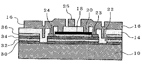
Referring to Fig.5, there is shown a cross sectional
view of the cross under portion 8 in Fig~.4. A pnpn-structure
constituting a three-terminal light-emitting thyristor is
constructed by stacking a p-type semiconductor layer 30, an
n-type semiconductor layer 32, a p-type semiconductor layer
34, and an n-type semiconductor layer 36 in this order on a
CA 02351368 2001-05-17
6
p-type semiconductor substrate 10. It should be noted that
the pnpn structure may be used in which an n-type
semiconductor layer, a p-type semiconductor layer, an n-type
semiconductor layer, and a p-type semiconductor layer are
stacked in this order on an n-type semiconductor substrate.
A lower metal wiring 18 is provided on the portion of
the pnpn-structure isolated in an islandl by a groove 22. The
lower metal wiring 18 is electrically isolated from the
substrate 10 by the pnpn-structure.
The lower metal wiring l8 is connected to an upper metal
wiring 16 through contact holes 20 opened in a insulating
film 14 deposited on the above described structure, resulting
in a cross under wiring. The upper wiring 16 and lower
wiring 18 constitute together one wiring, i.e. the ~2 wiring
3 (see Fig.4). One wiring 25 crossing to the ~2 wiring 3 in
Fig.5 corresponds to the cb l wiring 2 in Fig.4. In this
manner, the lower wiring 18 is electrically insulated from
the upper wiring 25 by the insulating .film 14, so that the
crossing of both wirings is possible.
As the self-scanning light-emitting device is based on a
thyristor of pnpn-structure, if a voltage is applied to the
pnpn-structure isolated in an island by a groove from the
metal wiring provided on the pnpn-structure, ~~latch-up
phenomenon" may be caused. When ~~lat~~h-up phenomenon" is
caused at the pnpn-structure, the thyristor may not only
operate normally, but also has a risk in that a large current
flows through the thyristor resulting in breakdown.
DISCLOSURE OF THE INVEN'.CION
An object of the present invention .is to provide a cross
CA 02351368 2001-05-17
7
under metal wiring structure which many prevent "latch-up"
from causing at a pnpn-structure.
The present invention is a cross under metal wiring
structure for a self-scanning light-emitaing device including
a self-scanning transfer element array having such a
structure that a plurality of three-terminal transfer
elements of pnpn-structure each having a control electrode
are arranged, the control electrodes of the transfer elements
neighbored to each other are connected via first electrical
means, a power supply line is connected to the control
electrodes via second electrical means, and clock lines are
connected to one of two terminals except the control
electrode of each of the transfer elements; and a light-
emitting element array having such a structure that a
plurality of three-terminal light-emitting elements of pnpn-
structure are arranged, the control electrodes of the light-
emitting element array are connected to the control
electrodes of the transfer element array, and a line for
applying a write signal connected to one of two terminals
except the control electrode of each c~f the light-emitting
elements is provided. The cross under metal wiring structure
is provided on the pnpn-structure isolated in an island by a
groove.
According to the present invenition, the following
approaches' can be taken to prevent "Latch-up" due to the
applied voltage from causing at a light-emitting thyristor of
pnpn-structure isolated in an island by a groove when a cross
under metal wiring is formed on the isolated pnpn-structure.
(1) It is intended that a potential difference is not caused
between the upper two layers of the pnpn-structure.
CA 02351368 2001-05-17
8
(2) The material of a lower wiring is selected so that the
lower wiring is made ohmic contact with the topmost layer of
the pnpn-structure.
(3) An insulating-type semiconductor layer is provided
between the topmost layer of the pnpn-si~ructure and the lower
wiring formed on the topmost layer.
(4) The topmost layer of the pnpn-structure is removed to
form a pnp-structure or npn-structure on which a lower wiring
is formed.
According to a first aspect of tlZe present invention,
the cross under metal wiring structu~__°e comprises a lower
wiring provided on a topmost layer of the pnpn-structure
isolated in an island by a groove, and an upper wiring
connected to the lower wiring through a first contact hole
opened in an insulating film covered the isolated pnpn-
structure and to a layer just below the topmost layer through
a second contact hole opened in the insulating film.
According to a second aspect of the present invention,
the cross under metal wiring structure comprises a lower
wiring provided on a topmost layer of the pnpn-structure
isolated in an island by a groove, and an upper wiring
connected to the lower wiring through a contact hole opened
in an insulating film covered the isolated pnpn-structure,
wherein the lower wiring is made of material which makes non-
ohmic contact with the topmost layer.
According to a third aspect of the present invention,
the cross under metal wiring structure comprises an
insulating layer provided on a topmost layer of the pnpn-
structure isolated in an island by a groove, a lower wiring
provided on the insulating layer, and an upper wiring
CA 02351368 2001-05-17
9
connected to the lower wiring through a contact hole opened
in an insulating film covered the isolai~ed pnpn-structure.
According to a fourth aspect of the present invention,
the pnpn-structure is changed into a ~pnp-structure or npn-
structure by removing a topmost layer of the pnpn-structure.
The cross under metal wiring structure comprises a lower
wiring provided on a topmost layer of the pnp-structure or
npn-structure isolated in an island by a groove, and an upper
wiring connected to the lower wiring through a contact hole
opened in an insulating film covered the isolated pnp-
structure or npn-structure.
BRIEF DESCRIPTION OF THE DiRAWINGS
Fig.l is an equivalent circuit diagram of a fundamental
structure of this self-scanning light-emitting device.
Fig.2 shows an element arrangement in a chip for the
self-scanning light-emitting device.
Fig:3 shows metal wirings around the bonding pad for ~1.
Fig.4 shows wirings formed in a two-layer structure.
Fig.5 is a cross sectional view of the cross under
portion in Fig.4.
Fig.6 is a cross sectional view of a cross under metal
wiring structure according to a firsit embodiment of the
present invention.
Fig.7 is a cross sectional view of a cross under metal
wiring structure according to a second embodiment of the
present invention.
BEST MODE FOR CARRYING OUT THE INVENTION
Embodiments of the present invention will now be
CA 02351368 2001-05-17
described in detail with reference to the drawings.
A first embodiment
Referring to Fig.6, there is shown a cross sectional
5 view of a cross under metal wiring structure of a first
embodiment. It should be noted that like components in Fig.6
are indicated by like reference numerals in Fig.5.
A p-type GaAs is used for a semi-conductor substrate 10,
a p-type GaAs for p-type semiconductor layers 30 and 34, an
10 n-type GaAs for n-type semiconductor layers 32 and 36, and
Si02 for an insulating film 14. A1 is used for upper wirings
16 and 25, and AuZn for a lower wiring :18.
According to the first embodiment" in order to prevent
"latch-up" in the pnpn-structure thyri.stor, it is required
that the potential difference is not caused between the upper
semiconductor layers 34 and 36'of pnpn-structure, i.e. the p-
type semiconductor layer 34 and n-type semiconductor layer 36
are at the same potential. For this purpose, electrodes 24
are provided on the p-type semiconductor layer 34, which are
made ohmic contact with the layer 34, and are connected to
the upper wiring i6 through contact holes 23 opened in the
insulating film 14, as a result the p-type semiconductor
layer 34 and n-type semiconductor layer 36 are connected
through the upper wiring 16. Therefore, the semiconductor
layers 34 and 36 are always at the same potential, thereby
the pnpn-structure thyristor consisting of the semiconductor
layers 30, 32, 34 and 36 never cause "latch-up phenomenon".
A second embodiment
Another method for preventing "latch-up" of a pnpn-
CA 02351368 2001-05-17
11
structure thyristor is to cause a latching current not to
flow through the pnpn-structure. For this purpose, in the
conventional structure shown in Fig.5, the material of the
lower wiring l8 is selected so as to make non-ohmic contact
(for example, schottky contact) with the topmost n-type
semiconductor layer 36 made of: n-type G<~As.
Concretely, AuZn is used for the :material of the lower
wiring 18: In this case, the rectifying characteristic of
metal-semiconductor (n-type) is a forward direction
characteristic when the metal side is at, a positive potential.
As this forward direction is opposite to the forward
direction of the pnpn-structure on the p-type substrate 10,
the latching current may not, be flowed through the pnpn-
structure.
It is desirable for the lower wiring 18 to use the same
material as that of electrodes for the p-type semiconductor
layer 34, because the fabricating procE~ss can be simplified
by forming the lower wiring 18 and the electrodes for the p-
type semiconductor layer at the same time.
A third embodiment
According to this embodiment, in t:he conventional metal
wiring structure shown in Fig.5, an insulating-type
semiconductor layer (not shown) is deposited on the pnpn-
structure, and the lower wiring 18 is provided thereon. Non-
doped GaAs may be used as material for the insulating-type
semiconductor layer.
In accordance with this structure, ~~latch-up phenomenon"
is not caused, because a voltage is not applied to the pnpn
structure due to the presence of the insulating-type
CA 02351368 2001-05-17
12
semiconductor layer on the pnpn-structure.
A fourth embodiment
In this embodiment, a lower wiring is isolated from a
substrate by a pnp-structure which corresponds to such
structure that the uppermost n-type semiconductor layer is
removed from the pnpn-structure.
Fig.7 shows a cross sectional view of a cross under
metal wiring structure of this embodiment. The lower wiring
18 is electrically isolated from the p-hype GaAs substrate l0
by the pnp-structure (30, 32; 34) that corresponds to the
structure in which the n-type GaAs layer 36 is removed from
the pnpn-structure in Fig.5. Adopting such pnp-structure,
the problem of "latch-up" inherent in the pnpn-structure
thyristor is not caused.
It should be noted that an npn-structure may also be
adopted in this embodiment.
While the present invention has explained with reference
to four embodiments, it is apparent for those who skilled in
the art that the present invention may be applicable to not
only a self-scanning light-emitting device but also a
semiconductor device base on a pnpn-structure.
INDUSTRIAL APPLICABIL:CTY
According to the present invention, it is possible to
prevent "latch-up" in the pnpn-structure when a cross under
metal wiring is formed thereon.