Note: Descriptions are shown in the official language in which they were submitted.
CA 02351454 2001-05-17
_. <
-1-
Measurement Assembly for Parallel
Readout of SPR Sensors
Description
The invention relates to a measurement assembly for parallel readout of
surface
plasmon resonance (SPR) sensors.
In the search for new active substances combinatorial chemical systems hold
high
promise in finding ligands matching a receptor molecule. Miniaturizing and
automating synthesis and parallelization thereof is salient to assaying as
large a
number of ligands as possible. Due to the small resulting amounts of ligand,
these
requirements (miniaturizing, automating and parallf;lizing) apply likewise to
detecting the ligand receptor binding for which the :high sensitivity of the
SPR
method can be used in which the light reflected from a thin gold film is
detected.
Under a suitable resonance condition (angle of incidence and wavelength of the
light and thickness of the gold film) the intensity of the reflected light is
reduced.
The energy of the light is then transformed into charge density waves of the
electron gas in the gold film, these charge density waves being termed
plasmons.
There are two methodical approaches to observing the resonance: either
monochromatic light is used in plotting the intensity of the reflected light
as a
function of the angle of incidence or the angle of incidence is maintained
constant
and the wavelength of the light is varied. In both cases the resonance curve
is
shifted with a change in the refractive index of the medium provided on the
side of
the gold film facing away from incident light.
This effect is made use of in biochemical analysis. The receptor or ligand is
immobilized on the gold surface. After addition of the ligand or receptor the
resonance condition is changed on molecular association.
The simplest assembly for measuring this effect is a glass prism which is
illuminated with light and the angle of incidence of which is varied (see e.g.
"Biospecific interaction analysis using biosensor technology" Malmqvist, M.,
Nature 361 (1993) 186-187).
A more sophisticated method is the parallel detection of multiple angles in
which
the gold surface is illuminated with a slightly divergent beam of
monochromatic
light (aperture angle ~ 10°) and the reflected light i:~ directed to a
position
resolving light detector for obtaining an explicit assignment between the
angle of
reflection and the position on the detector. This construction has the
advantage of
CA 02351454 2001-05-17
-2-
sensing the angle range of interest with no moving parts. This is why use is
made
of this kind of detection in a few commercial systems as disclosed e.g. in WO
90/05295 Al or EP 797 091 Al. One disadvantage of these assemblies is that
only
one prepared array of gold sensors (one-dimensional detection) or but a few
arrays
of sensors arranged along a line (using a two-dimensional detection) can be
assayed each time, i.e. this not permitting simultaneous measurement of a two-
dimensional sensor array by this angle detection method. After having
installed the
prepared gold film in systems of this kind, obtaining thermal equilibrium
takes,
however, some minutes (at least 15 minutes), i.e. th.e actual measurement then
lasting at least until equilibrium of the molecular association is attained
which may
also take up some minutes. This is why systems of this kind lack good
suitability in
detecting the binding of a large number of different ligands, since the time
and
expense involved in measuring and changing the samples is relatively high.
A parallel approach to analyzing a sample array is ;iPR microscopy (SPM) (see:
EP 388 874 A2 or M. Zizisperger, W. Knoll, Prog Colloid Polym Sci.1998, 109
pages 244-253) in which the gold surface applied to a prism is coated in
various
portions with various samples and the gold surface imaged on a CCD chip at the
SPR angle. During measurement the angle is varied by a mechanical scanner.
However, this method is restricted to small object diameters.
A more recent SPR method is disclosed in WO 94/1.6312A1 in which detecting the
binding of small amounts of substance is achieved by optical fiber guides
partially
coated with a gold film. However, here too, the problem still exists in
designing a
system required to assay a plurality of samples in parallel in accordance with
this
principle. Such an array of gold-coated fibers is, on the one hand, expensive
and
highly sensitive to mechanical stress, and, on the other, producing the array
in
parallel as proposed therein is difficult to achieve technically.
Optical fiber guides are also employed as it reads from WO 98/32002 A1. To
protect them from being damaged physically the fiber cable is housed in a
pipette.
To achieve an array it is proposed to use a series arrangement of such
pipettes.
However, miniaturizing such an arrangement is difficult to achieve, especially
for
parallel measurement of many different samples.
Known from DE 196 15 366 A1 is a method and a means for the simultaneous
detection of physical, biological or biochemical reactions and interactions at
or in
the surface of samples. All samples are simultaneously illuminated with
CA 02351454 2001-05-17
-3-
monochromatic light and the reflected light supplied to a detection array,
e.g. of a
CCD matrix or video camera. The samples may be matrixed with the sensor
surface areas in a single plane on a substrate plate located in turn on a
transparent
base plate which is illuminated. The electrical signals of the detection array
are
supplied to an analyzer. After analyzing the samples at one wavelength, the
wavelength can be set to another value.
Known from WO 95/22754 is an analyzer in which a plurality of SPR analysis
wells are arranged in a matrix for simultaneous assaying. The sensor surface
areas
of the analysis wells are located parallel in a single plane.
The invention is based on the object of defining a measurement assembly for
simultaneous readout of a plurality of SPR sensors, more particularly
exceeding a
hundred or a thousand, in which readout is completed with a measuring time of
less than thirty minutes.
This object is achieved by the measurement assembly and the measurement
method as set forth in the independent claims, advantage aspects reading from
the
sub-claims.
To achieve this object, use is made of a specially configured array in an
assembly
with imaging methods to permit simultaneous readout. The array used for this
purpose comprises a plurality of waveguides, it being noted that waveguide in
this
context is understood within the scope of the present invention to be an
optical
medium in which the light is guided in at least one dimension and which has at
least two parallel interfaces.
The invention will now be detailed by way of examples illustrated diagramma-
tically in the drawings in which:
Fig. 1 is an illustration of one variant of part of a waveguide array
employed,
Fig. 2 is an illustration of how a single SPR-compatible sensor element is
assigned
to the pixels of a CCD array
Fig. 3 is an illustration of a first variant of a measurement assembly in
accordance
with the present invention
Fig. 4 is an illustration of a second variant of a measurement assembly in
accordance with the present invention
CA 02351454 2001-05-17
-4-
Fig. 5 is an illustration of a third variant of a measurement assembly in
accordance
with the present invention
Figs. 6a and 6b are illustrations of two different optical beam paths through
the
SPR-compatible surface area,
Fig. 7 is a CCD image of a SPR waveguide array,
Fig. 8 is a plot of the intensity profile of a single SPR-compatible
waveguide,
Fig. 9 is a plot of how the intensity profile is shifted for differences in
the sample
concentration and
Fig. l0a and b illustrate the difference between illuminating the waveguide
array
with divergent light in accordance with one embodiment as shown in
Fig. 4 and with parallel light as shown in Fi;~s. 3 and 5.
Referring now to Fig. 1 there is illustrated how use is made to advantage
within the
scope of the present invention of a planar SPR sensor 1 suitable for being
fabricated by known silicon semiconductor technologies and arranged into a
waveguide array. Part of one such waveguide array is shown in Fig. 1. A wafer
of
silicon 11 is provided with a layer of Si02 12 serving as an optical buffer
relative
to the waveguiding layer 13 and the silicon base material 11. The waveguide
consists of a layer of silicon oxynitride 13 in a thickness down to approx. 10
~.m.
The silicon oxynitride layer 13 is patterned by a dry etching process so that
parallel
strips 14 materialize having widths in the range 10 dam to 2000 ~m on a center-
spacing in the range 10 ~,m to 5000 Vim. Once the waveguide strips 14 have
been
patterned, the complete wafer is protected by a covE;r (not shown) except for
the
areas intended to form the substrate for the SPR-compatible metal layer 16 in
a
later process. Subsequently, the exposed locations of the waveguide left
unprotected in the previous step in the process are metallized in a thickness
compatible with the requirements of the SPR measurement. The remaining cover
of the wafer is removed. Depending on the technology employed for producing
the
comb-like recesses 15 in the substrate, these recesses may be produced before
or
after cited metallization.
The technology as described permits accommodating a plurality of parallel
arrangements of waveguide patternings on a wafer which are then singled by
means of etching silicon or sawing the silicon wafer. Separating each
waveguide
from the other, at the end locating the SPR sensor, is achievable by wet
chemical
etching the silicon or by a sawing process. Another variant in producing the
waveguides consists of the possibility of producing polymers in thin films
e.g. by
CA 02351454 2001-05-17
-5-
centrifuging them onto a substrate. The polymers (~e.g. PMMA, polycarbonate,
UV-curing adhesives or siliconated polymers (cyclotenes or ORMOCERES))
present in dissolved or non-cured form are centrifuged or poured onto the
substrate
material. The refractive index of the substrate material must be smaller than
that of
the polymers to be applied, later representing the waveguide. When using UV-
curing polymers, after homogenous application of i:he layer, the non-exposed
portions are etched away so that narrow parallel strips of polymer remain on
the
substrate. Other polymers may be produced as strips by embossing or other
replication techniques, the material remaining at the locations at which no
light is
to be guided needing to be dimensioned correspondingly thin. After the
waveguide
strips have been patterned, here too the complete wafer is protected by a
cover
except for the areas intended to carry the SPR-compatible metallization 16. In
the
next step these exposed areas are coated with the SIPR-compatible
metallization 16,
after which the protective layer covering the remaining areas is removed.
The variants described permit production of a great many waveguides in
parallel
on a wafer. After fabrication of the waveguides with the SPR sensor surface
areas,
single strips consisting of a plurality of parallel waveguides are prepared
from the
processed wafer by a separating method, e.g. sawing. This singling process
results
in new face areas 17 which are prepared so that light can be coupled thereinto
and
thereout o~
The variants as described permit planar fabrication of a great many SPR
sensors
arranged in a row. To achieve an array of sensors several of these strips are
arranged stacked horizontally. After assembly, such an array can be casted in
a
portion outside of the SPR-compatible metallization in a polymer to provide
the
SPR waveguide array with additional support. The arrangement and spacing of
the
individual SPR-compatible sensors may be made in accordance with the
arrangement and spacing of the wells of a microtiter plate 60 (see Fig. 3) to
be
presented. When this is the case, the SPR waveguide array is brought into
contact
with the microtiter plate 60 carrying the samples 61 to be characterized, for
measuring or coating the SPR-compatible layers 16 by introducing the SPR
waveguide array into the microtiter plate 60 sufficiently until the SPR-
compatible
metallization is totally wetted by the samples 61. The individual vertical
arranged
waveguides can be arranged horizontally on the center-spacing of an optional
microtiter format.
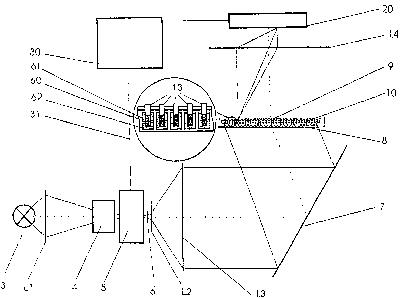
A waveguide array of the aforementioned kind is made use of in a first variant
as
will now be described with reference to Fig. 3.
CA 02351454 2001-05-17
-6-
Referring now to Fig. 3 there is illustrated how only light in a bandwidth of
approx. 0.5 to 5 nm is transmitted from the white light of a halogen lamp 3
after
having passed through a suitable beam adapter optical system L1, an IR filter
4
inserted in the example to protect the optical components and a monochromator
5.
As an alternative, selecting the wavelength may also be implemented with a
filter
wheel, requiring a corresponding number of filters having a similar bandwidth.
Thereafter, in the example, the polarization direction is selected by a
polarisator 6
for TM waves in respect of the SPR-compatible me;tallization 16 of the
employed
optical waveguide 13. An optical beam spreader L2, L3 then ensures parallel
illumination of the complete waveguide array, in this example, via a folding
mirror
7 applied so that the light is incident in the waveguide 13 at an angle of
70° to 90°
relative to the normal of the gold film of the waveguides, since it is only
light in
this angle range that is capable of exciting plasmon resonance. Using a
folding
mirror in this case merely serves to make for a more compact configuration of
the
measurement assembly. As an alternative, illumina~,tion could also be made
directly
at this angle. A perforated mask 8 provided in the example as shown in Fig. 3
which may take one of many configurations, shades the portions behind which no
waveguide is located to prevent scattered light from gaining access by some
unwanted way to a detector furthermore provided. 'JVhen some other
technologically more complicated means of applying and locating a plurality of
waveguides arranged in parallel is provided, as corrunercially available with
a core
diameter of approx. 200 Vim, for example by embedding the individual waveguide
sections in a common substrate, likewise in the scope of the present
invention, then
use may be made of a non-transparent material or a material having a non-
transparent coating for the substrate material employed, as a result of which
the
perforated mask 8 as mentioned above can be eliminated. The waveguides
themselves are located by their sensitive portion in a liquid which can be
changed
for implementing reference measurements in the various solutions to swap the
target molecules or to implement washing. At the end of the waveguide remote
from the sensitive waveguide portion the light emerges at an angle the same in
amount as that with which it was incident into the other side (see Fig. 6). In
the
scope of the invention a dispersing means 9 is furthermore assigned to the
waveguide sections at the light exit end, causing dispersion of the light
emerging
from the waveguides. This is achievable, for example, by means of a dispersing
lamella to be applied separately, a suitable coating, or the like. This
strongly
divergent light is imaged directly by the objective lens L4 on a CCD chip 20,
the
objective lens L4 being designed to "see" the entirety of the waveguide array,
but
CA 02351454 2001-05-17
'rc'
_7_
only a small proportion of the light emitted from an optical waveguide
permitting
detection. For detecting such small amounts of light, use is made in the
example of
a cooled high-sensitivity CCD chip 20, the necessary exposure time of which
may
amount to a few seconds.
It is provided for in the scope of the present invention that the light
emerging from
each waveguide is imaged on several CCD pixels simultaneously to enhance
accuracy of detection. Thus, in the example, imaging is provided for on
several
camera pixels since a CCD chip has a great many more pixels than the waveguide
array provided for in this case at the individual waveguides. Within the scope
of
the present invention, an image processing software; is employed for assigning
the
portion of several CCD pixels to each waveguide. This is indicated
diagrammatically in Fig. 2, e.g. waveguide 2,2 being assigned the pixel
portion
{(11,12), (11,13), ...,(14,13)}, i.e. the portion of the CCD chip 20 for
imaging the
waveguide 2,2 comprises 12 pixels. This assignment is memorized in a computer
30 and remains available for the complete duration ~of the subsequent
measurement, since the array is no longer moved further. A fast program
algorithm
obtains the sum of these camera pixel portions assigned to each waveguide so
that
a discrete intensity value is obtained and memorized for each waveguide. The
wavelength of the light incident from underneath in the example, is then
shifted by
approx. 1 nm with the aid of the monochromator 5 signalled by the computer 30
to
obtain the next intensity value for all waveguides to thus obtain an intensity
spectrum specific to each and every waveguide. To optimize the measuring time
needed for imaging such a spectrum, the exposure of the CCD camera is
instantly
restarted, once the data relative to the last wavelength have gained access to
the
computer memory and a new wavelength is set at a ~monochromator 5 signalled by
a stepper motor. Summing the results in the computer as to the pixel maps can
then
be undertaken during the time needed for exposing the new wavelength, When
this
time is sufficiently long, the time needed for compu~.ing the summation is
negligible. The time needed for each wavelength is dictated substantially by
the
exposure time, which in the example is approx. 5 seconds, 16 minutes thus
being
needed for a spectrum of 200 nm. Now, to determine; the molecules associating
with each SPR sensor of every individual waveguide, it is not the absolute
intensity
spectrum of a single measurement, but the difference in the minima of the
intensity
spectra for a measurement in a pure buffer solution as compared to those of a
second measurement in the presence of the target molecule, i.e. it is this
shift in the
wavelength that first permits arriving at an indication as to the molecular
CA 02351454 2001-05-17
_8_
association. Accordingly, sequencing reference and sample measurements would
be possible within 32 minutes for all waveguide sensors illuminated.
Referring now to Fig. 4 there is illustrated diagrammatically another variant
of the
assembly in accordance with the invention which reduces the time needed for
the
measurement. Since it is the time needed for the exposure which is the time-
limiting factor, the measurement time can be shortened by increasing the
amount
of light in the waveguides. For this purpose a more powerful light source 3,
such as
e.g. a Xenon arc lamp may be employed, The same as in the arrangement as shown
in Fig. 3, the light first passes through an IR filter 4, a monochromator 5
and a
polarisator 6, an optical beam spreader L2, L3 then assuring parallel
illumination
of the waveguide array 10, upstream of which in this embodiment spherical or
gradient lenses LS are inserted. To illuminate all waveguides in the example
as
shown in Fig. 4, however, several new positionings of the waveguide array 10,
relative to the lenses LS provided, are needed. However, assigning a separate
lens
to each waveguide is likewise within the scope of the present invention
whereby
this lens may also be a component in the wells 62 of the microtiter plate
concerned.
The parallel light is focussed by the lenses LS into the waveguides, coated
with
gold, for example, such that in the sensitive portion of the waveguide the
diverging
rays are incident at the provided metallization of the waveguide also at the
angle
permitting SPR detection. As compared to the exposure arrangement as shown in
Fig. 3 the lenses LS as provided in the example permit inputting roughly 100
times
the light intensity into the waveguides. The entrance; windows 17 of the
waveguides in this example are positioned at the focal point of the lenses,
i.e. at a
distance of a few 100 ~.m. In this arrangement it is to be assured that no
light
bypasses the waveguide, for instance due to any interspaces or transparencies,
into
the space for light exit from the waveguides. Here too, this can be avoided by
providing the means as described above, for example a perforated mask 8. At
the
light exit end of the waveguides the light emerges from the optical waveguide
again divergent and is likewise imaged on a CCD chip 20 with the aid of a
dispersing means 9 and an objective lens L4.
The further assignment and analysis of the light intensities assigned to each
optical
waveguide is the same as described with reference to Fig. 3. For each
wavelength,
the time needed can now be reduced to approx. 1 second due to the higher light
intensity. When restricting the arrangement to e.g. a spectrum of sixty
wavelengths, the time needed for measuring all spectra in parallel in the
example is
one minute, thus making it possible to implement e.g. kinetic binding assays
simultaneously with a large number of ligands.
CA 02351454 2001-05-17
_g_
Referring now to Figs. l0a and l Ob the difference lbetween illuminating the
waveguide array 10 with divergent light in accordance with the embodiment as
shown in Fig. 4 and with parallel light as shown in Fig. 3 will now be
demonstrated. These Figs. illustrate the marginal rays after having passed
through
the perforated mask 8 against the background of a l'.ine of sensors. In the
divergent
case (Fig. l0a) the marginal rays sweep several measuring ranges so that after
emergence the marginal ray can no longer be assigned to a single measuring
range, this being the reason why when illuminating with divergent light,
interfaces
40 are to be included at the margin of the sensor area to ensure total
reflection,
whereas when illuminating with parallel light (Fig. l Ob) these margin areas
can be
eliminated. In this arrangement the light beam is g~:~ided solely by total
reflection at
the sensor area and the opposite surface. In this case the light beam
penetrates the
waveguides at a angle suitable for SPR resonance right from the start. When
then
being successful in imaging the entirety of the parallel emergent light on a
CCD
detection, it is likewise possible to increase the intensity and thus to
shorten the
time needed for measurement, except that in this case unlike the situation as
shown
in Fig. 3, the angle of the incident light is fixedly defined.
Referring now to Fig. 5 there is illustrated a more complicated embodiment,
working on the principle of total parallel ray path aazd achieving
additionally
improved imaging performance (less edge shading, lower sensitivity to
scattered
light). In this case the light is guided through an optical fiber 50 via an
optical
imaging system L1,L1' to the monochromator 5 an<i through a further optical
fiber
51 to an optical beam spreader L2, L3. This has the advantage that guiding the
illuminating beam can be adjusted independently of the light being coupled
into
and out of the monochromator 5. Illuminating the waveguide array 10 is done
the
same as described in Fig. 3 with a spread parallel bundled rays at the plasmon
resonance angle, a perforated mask (not shown in Fig. 5) being employed
optionally as shown in Fig. 3. In emerging from the sensor the light is either
parallel displaced (for an even number of reflections, cf. Fig. 6b) and thus
at the
angle a, the same as on entry, or for an uneven number of reflections (Fig.
6a) it
emerges at an angle -a. The length L and width B oil the SPR-compatible
waveguide are specially dimensioned in the example as shown in Fig. 5 so that
the
number of reflections is uneven and thus the light emerges exclusively in the
direction of a second folding mirror 71. Unlike the situation as shown in Fig.
3 in
which imaging on a CCD camera is achieved with a scattering layer, in this
case
the parallelism of the emerging light is made use of to practically reverse
the
illuminating light path. Via an achromatic collimator lens L6 of long focal
length
CA 02351454 2001-05-17
,.;,. s.,,
-10-
(e.g. f--1000 mm) and large diameter and a suitable. objective lens L7 (e.g. f-
-100
mm) the surface area of the sensor array is imaged on the CCD chip like in a
telescope. Since the surface of the waveguide array 10 to be imaged does not
stand
perpendicular to the optical axis of the arrangement, using a conventional
camera,
i.e. with the objective lens parallel to the CCD chip would result in only a
line of
the object being sharply focussed because of the inadequate depth of focus.
This is
why on the imaging side the CCD chip 20 needs to be likewise tilted relative
to the
optical axis, as indicated in Fig. 5, to ensure a sharp image of the whole
sensor
array surface area 10. This is achievable by tilting the CCD camera with a
goniometer (not shown) relative to the objective lens.
Another advantage of telescopic imaging is its low sensitivity to scattered
light,
since it is only the light emerging at the detection angle from the plane of
the
object that is imaged on the CCD chip.
Referring now to Fig. 7 there is illustrated a sharp ionage of a sensor array
10 as
produced by the optical arrangement as shown in Fig. 5. Such an image is
detected
for each wavelength and in the computer 30 the intensity integral as a
function of a
sensor surface area is formed, as described above with reference to Fig. 2. It
is in
this way that for each and every sensor a drop in the; intensity as
materializing in
surface plasmon resonance, is detected in the spectrum as shown in Fig. 8 by
way
of example for a single case. The broken line curve in the upper portion of
Fig. 8
shows the spectrum with the sensor surface area located in air, this
substantially
corresponding to mathematically folding the lamp spectrum and monochromatic
transmission. The solid line corresponds to the measurement in the presence of
a
buffer; this spectrum is superimposed by the surface; plasmon resonance. As
shown
in the lower portion of Fig. 8 obtaining the pure surjPace plasmon resonance
spectrum is done by scaling to the spectrum in air.
To verify that the detected drop in the spectrum is surface plasmon resonance,
the
refractive index of the solution is varied by making the measurement in
various
sucrose concentrations. It is evident from the upper ;portion of Fig. 9 how
the drop
in the spectrum is shifted, as expected, with increasing sucrose
concentration.
Adapting the measurement data with a Gauss function furnishes numerical values
for the location of the minima of the spectra, from which, with the known
refractive index of the solution, a calibration curve is obtained as shown in
the
lower portion of Fig. 9. For a sufficiently small range of the refractive
index an
approximately linear relationship is assumed. In the present example a shift
of 1.4
nm is obtained for a change in the refractive index of 10-3 in enabling the
minimum to be determined with an accuracy of approx. 0.3 nm, a typical value
for
CA 02351454 2001-05-17
...> ~ ::~w"~
-11-
a resonance curve of approx. 50 nm half value width. Thus changes in the
refractive index of 2 ~ 10-4 can be detected. This demonstrates the
sensitivity of the
method for parallel measurement of several hundred or thousand samples within
a
few minutes.
CA 02351454 2001-05-17
m
-12-
List of Reference Numerals
1 - planar SPR sensor
- waveguide array
11 - wafer of silicon
12 - Si021ayer
13 - optical waveguide
14 - waveguide strips
- comb-like recesses
16 - SPR-compatible layer
17 - face areas (entrance windows)
of 13
- CCD chip (camera) 20
3 - light source
4 - IR filter
5 - wavelength-selective assembly
6 - polarisator
7 - folding mirror
71 - second folding mirror
8 - perforated mask
9 - light dispersing means
- computer
31 - control line
- reflective interfaces
50,51 optical fiber
-
60 - microtiter plate
61 - sample in a well of a microtiter
plate
62 - wells
B - width of SPR-compatible waveguide
L - length of SPR-compatible waveguide
a - angle of light entry/exit
Ll,LI',L2,L3,L4,L6,L7
- optical
imaging
systems
LS - lenses