Note: Descriptions are shown in the official language in which they were submitted.
29-01-2001 CA 02351573 2001-05-15 PCT/CA99/0083~
Voltage Sensor
Field of the Invention
The present invention relates - to a voltage sensor for measuring voltage and
is
particularly suitable for measuring high voltages such as on high-voltage
power transmission
lines.
Background to the invention
The list of known high-voltage voltage transducers includes inductive
transformers,
capacitive dividers or capacitive voltage transformers, and transducers using
bulk-optic electric
field sensors. The first two transducers suffer from bandwidth restrictions,
expensive failure,
extensive maintenance, heavy weight, and output variations. They also suffer
from the need for
substantial insulation that is both expensive and potentially hazardous to the
environment (e.g.
oil and/or SF6 gas).
US patent 4,939,447 issued July 3, 1990 to Bohnert et al (see also the paper
"Fiber-optic
sensing of voltage by Iine integration of the electric field" Optics Letters,
vol.4, no.5, March l,
1989, pp. 290 - 292) describe a voltage sensor that uses multiple fiber-optic
piezoelectric
electric field sensors to measure voltage. Accuracy is obtained by the use of
a plurality of
sensors r.e, the Optics Letters publication indicates that to obtain
reasonable accuracy 22 sensors
connected in series was required.
Pockels cells are known devices that have been used for measuring voltage
particular-ly
high voltage, for example see US patent 5477134 issued to H. Hamada and US
patent 5731579
issued to G.K. Woods. A preferred form of Pockets cell for use in the present
invention is an
integrated optics Pockets cell such as that described in US patent 5,029,273
issued July 2, 1991
to Jaeger, the disclosure of these, and others, being well known to those
skilled in the art.
Brief description of the preseat invention
The present invention reduces significantly the deficiencies inherent to the
existing hi h-
g
voltage transducer technology. The simple structure of the invention removes
the need for
expensive and/or environmentally unfriendly insulation; may be made lighter,
allowing for less
expensive transportation, installation, and maintenance; and is compatible
with existing standoff
structures, allowing for easy construction.
AMENDED SHEET
CA 02351573 2001-05-15
WO 00/34793 PCT/CA99/00835
2
When used with compact electric field sensor technology, such as the
integrated optics
Pockets cell, the invention offers wide bandwidth and easy interfacing with
emerging digital
technology.
Broadly the invention relates to a method of measuring the value of voltage
difference
between two points to provide a measured value V of said voltage difference
comprising
measuring electric field at at least one location in space to provide a
measured value of electric
field E for each of said at least one location and using a mathematical
combination of the value
of electric field E for each of said at least one location, said combination
being arranged and
said at least one location being chosen so that for any given value of said
voltage difference
between said two points any practical disturbance in electric field
influencing the measured
value E does not significantly change the measured value V of said voltage
difference.
Broadly the present invention also relates to a method of measuring value of
voltage
difference between two points to provide a value V of said voltage difference
comprising
choosing at least two locations spaced distances x; from one of said two
points, measuring and
providing values of electric fields E; at said at least two locations,
applying weighting factors oc;
to said measured electric fields E; at said corresponding positions spaced
their respective
distance x; from said one point to obtain a value V based on
n
v = ~ alET
wherein
n = the number of electric field sensors and is at least 2
x; and a; are selected so that dE; representing any changes in E; measured at
said
at least two locations spaced their respective distance x; from said one
point, due to
external disturbances, are compensated for so that they do not materially
affect said
value V, so that the value of
n
~, a ; ~ r
r=1
SUBSTITUTE SHEET (RULE 26)
CA 02351573 2001-05-15
WO 00/34793 PCT/CA99/00835
3
is sufficiently small, and
x; and a; are obtained by a method selected from the group consisting of trial-
and-error, mathematical or computer modeling.
Preferably x; and a; are determined using a quadrature method or an
integration formula.
Preferably the quadrature method is a Gaussian quadrature.
Broadly the present invention relates to an apparatus for measuring voltage
comprising
an electrically isolating section between a pair of spaced conductors defining
opposite ends of
IO said isolating section between which voltage difference is to be measured,
at least one electric
field sensor which measures electric field at at least one location within
said isolating section,
said isolating section having a relative dielectric permittivity and geometry
which provides
sufficient screening of said at least one location from other electric field
sources external to the
isolating section so that said external electric field sources of practical
strength do not materially
change said at least one electric field measured at said at least one
location.
The present invention relates to an apparatus for measuring voltage comprising
an
electrically isolating section between a pair of spaced conductors defining
opposite ends of said
isolating section between which voltage difference is to be measured, at least
one electric field
sensor which measures electric field at at least one location within said
isolating section, said
isolating section having a relative dielectric permittivity and geometry which
provides sufficient
screening of said at least one location from other electric field sources of
practical size external
to the isolating section so that the error in voltage difference measured
under presence of said
external sources of electric field is less than 6%.
Preferably, the error in said voltage difference measured is less than 1%,
more preferably
less than 0.3%.
Broadly the present invention relates to a method and apparatus for measuring
voltage
comprising an essentially electrically isolating section between a pair of
spaced conductors
between which voltage difference is to be measured. At least one electric
field sensor is
positioned within the isolating section. The isolating section has a
permittivity and size
sufficient to provide screening of the field sensor from other electric field
sources external to the
SUBSTITUTE SHEET (RULE 26)
CA 02351573 2001-05-15
WO 00/34793 PCTlCA99/00835
4
isolating section so that the other electric field sources do not materially
affect the voltage
measurement.
Preferably the electric field sensor is an integrated optics Pockels cell.
Preferably the relative dielectric permittivity of the section is greater than
2, mare
preferably greater than 20.
Preferably the isolating section is a hollow isolating section in which the
electric field
sensor is mounted.
Preferably there is one said electric field sensor positioned in said
isolating section
spaced from one of the conductors a distance of between 25 and 75% of distance
L between the
pair of conductors.
Preferably there are a plurality of the electric field sensors positioned in
the isolating
section in spaced relationship along a longitudinal axis of the isolating
section between the two
conductors.
Preferably the number of electric field sensors in the isolating section is
two, a first
sensor positioned in said isolating section spaced from the one conductor by a
distance of
between 50 and 100% of distance L between the pair of conductors and a second
electric field
sensors positioned in the isolating section spaced from the one conductor by a
distance of
between 0 and 50% of distance L between the pair of conductors.
Preferably the number of said electric field sensors in the isolating section
is three, one
positioned in said isolating section spaced from the one conductor a distance
of between 70 and
100% of distance L between the conductors, another electric field sensor
positioned in the
isolating section spaced from the one conductor by a second distance of
between 30 and 70% of
distance L between the pair of conductors and yet another electric field
sensor positioned in the
isolating section spaced from the one conductor a third distance of between 0
and 30% of
distance L between the pair of conductors.
Preferably the number of sensors in the isoiating section will not exceed 9.
Preferably said electric field sensors collectively occupy less than 10%, more
preferably
less than 2% of the distance L between the conductors.
Brief description of the drawings
Further features, objects and advantages will be evident for the following
detailed
description taken in conjunction with the accompanying drawings in which
SUBSTITUTE SHEET (RULE 26)
CA 02351573 2001-05-15
WO 00/34793 PCT/CA99/00835
Figure 1 illustrates the basic structure of the invention.
Figure 2 illustrates a basic unperturbed Electric Field Sensor Voltage
Transducer (EFS
VT) structure of the present invention in front and side views as it may be
installed in a high-
voltage substation.
5 Figure 3 shows three basic EFS VT structures each using three field sensors
in a three-
'phase high-voltage transmission system.
Figure 4 shows plots of in-phase p; (x) and out-of phase po (x) of an example
for the
case of the standoff structure with E1= 40 at Phase A.
Figure 5 is similar to Figure 3 but further schematically illustrating an
arrangement
wherein a vertical semi-infinite ground plane is placed spaced from Phase A of
a three-phase
transmission system (by a distance of one meter in this example).
Figure 6 is a plot illustrating the affect of relative permittivity (cl) of
the dielectric
shielding on electric field distribution inside the isolating section.
Figure 7 is a section along the line 7 - 7 of Figure 1. showing the sensor
positioned on
the axial center line of the dielectric column.
Figure 8 is a section through the sensor (e.g. an integrated optics Pockels
cell) along the
line 8 - 8 of Figure 7
Figure 9 is a side elevation of the sensor looking from the right in Figure 7.
Figure 10 is a view similar to Figure 1 showing a modified version of the
invention
Figure 11 shows another embodiment of the invention showing the use of a solid
rod (as
opposed to the hollow column) to form the isolating section.
Description of the preferred embodiments
The invention as schematically shown in Figure 1 and 2 applied to a standoff
11 is
formed by a column or isolating section 10 supported on a cylindrical metallic
(current
conducting) stand 12. Electric field sensors (EFS) 14 (three shown but only
one is necessary
and more may be used if desired) are mounted in the column 10 and are
protected by the column
10 from the outside environment. The isolating section 10 is interposed
between (in the
illustrated arrangement of Figure 2, 3 and 5) a power line 18 and the metallic
stand 12
connected to ground schematically indicated at 15 between which the voltage is
to be measured.
The isolating section 10 containing electric field sensors may be positioned
between and
connected to any two conductors between which the voltage is to be measured.
SUBSTITUTE SHEET (RULE 26)
CA 02351573 2001-05-15
WO 00/34793 PCT/CA99/00835
6
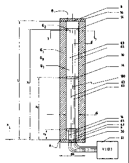
In the embodiment shown in Figure 1 the column 10 has been shown as a hollow
cylinder with an outside diameter do, an inside diameter d;, and a length L.
Obviously if the
column 10 is not hollow, the inside diameter d; is zero (0). The thickness d
of the dielectric
material between the sensor 14 and the ambient surroundings in effect defines
the thickness of
S the dielectric material shielding the sensor 14 which coupled with the
permittivity of the
dielectric material defines the shielding and as discussed below with respect
to Figure 6
influences the structure of the electric field.
In the Figure 10 embodiment the isolating section 10 is formed by a laminate
of a
number of dielectric layers 145, 150, 155, 160, 165 and 170 (in the
illustrated case, hollow
cylindrical layers) that may have the same or different permittivities as
indicated by the relative
permittivity symbols si, E3, sa, Es, Es, and g~. For example, the layers 145,
155 and 165 may be
air. Obviously the number of layers and the permittivity of each layer or the
combined
permittivity of all the layers may be changed to suit the application, as
desired. Preferably si,
and s4 will be greater than so, ss, and E5. The relative permittivity so is
the relative permittivity
of the surrounding atmosphere and E2 that of the material in which the sensor
is encapsulated.
It will also be noted that the outer layer 170 may be of non-uniform thickness
demonstrating that the thickness of the isolating section 10 need not be
uniform.
One of the simplest ways to build the isolating section 10 is to stack a
plurality of
discrete axial portions (measured parallel to length L) some of which termed
modules will
incorporate the EFS(s) and simply fix the portions and modules together to
construct the section
10 with the modules containing the EFS(s) in the desired locations along the
length of the
section 10 i.e. the section 10 could be made of portions i.e. slices
(different thickness andlor
hollow) with the modules) being slices in selected locations along the axial
length of the
section 10.
The length L for any installation depends on many factors the most important
is safety
and then accuracy. The length L should be held to a minimum for accuracy,
however for safety
it cannot be too short. The values (e.g. the distance from high voltage (H~
line to ground) will
be chosen so that the electric field anywhere inside, near, and outside the
structure is not greater
than the break-down strength (field) of the materials) present at that
location under any
reasonable operating condition as provided by gaverning bodies such as the
Institute of
Electrical and Electronics Engineers (IEEE), the American National Standards
Institute (ANSI),
SUBSTITUTE SHEET (RULE 26)
CA 02351573 2001-05-15
WO 00/34793 PCT/CA99/00835
7
the International Electro-technical Commission (IEC), and/or other local and
international
standards, i.e. the length L will be set to meet the required local and
international standards.
When a source of voltage is applied to the top 16 of the column 10 e.g. when
16 is
connected to a high-voltage Iine 18 the dielectric material from which the
section is constructed
causes a structured electric field distribution in and around the column 10.
As the relative
permittivity (E1) of the material is increased as shown in Figure 6 the
structure of the field
distribution changes i.e. the field distribution changes to be more uniform
(compare gi = 10 with
E1= 100). Though the system is operative with relative permittivity s~ = 1,
the overall accuracy
of the system improves if the permittivity is greater i.e. the field
distribution is made more
uniform, and external influences are reduced, thus, generally the permittivity
of the section 10
will be at least 2 and preferably at least 20.
Measurement of the electric field by each of the at least one strategically
placed electric
field sensor 14 is delivered via lines schematically indicated at 63 (e.g. a
pair of lines 63 for
each sensor 14 (see figure 1)) to a suitable computing means 61 which may be
in the form of a
suitable chip or the like which as will be explained herein determines the
voltage difference V
between point b at one end (top 16) and point a at the opposite end of the
column or section 10
(top of plate 30).
The sensors 14 are strategically placed in the isolating section 10 to tend to
minimize
error in the measurement (determination) of the voltage difference. The
preferred placement of
the sensors) can be determined by any suitable method for example by trial-and-
error but the
quadrature method as will be described herein below is the preferred method of
determining the
placement of the sensors. The end result of proper placement and selected
compensation for
distortions in the electric field distribution is that for the present
invention typical distortions in
the electric field distribution do not significantly affect the reported
voltage measurement value
V.
Typical causes for distortions or perturbations include the presence of other
conductors
at other potentials, e.g., in a high-voltage three-phase system, the presence
of other two phases
can be considered a cause of a perturbation. These distortions also include
the effects of
pollution on and around said isolating section or column 10 and its sheds, if
any, and other
nearby structures, conducting or non-conducting, mobile or stationary. Of
course, these other
SUBSTITUTE SHEET (RULE 26)
CA 02351573 2001-05-15
WO 00134793 PCT/CA99/00835
8
structures are usually located at a distance determined using various relevant
IEEE, ANSI, IEC,
andlor other standards or guidelines on each voltage class.
Also, "significantly" as used in the above statement, or other words such as
"materially"
or "sufficiently," is defined using appropriate IEEE, ANSI, IEC, and/or other
standards or
guidelines available for specific applications. For example, for revenue
metering in North
America, VTs are typically required to have errors less than 0.3%; so, in such
a case where a VT
is to be used as a part of a revenue metering system, the statement "do not
significantly affect
the reported voltage measurement value" means that "the reported voltage
measurement value is
within ~0.3% of the actual voltage." Obviously, for other applications, or
other standards, the
terms "significantly" or "sufficiently" or "materially" correspond to other
numerical values.
Another example is a VT that has to meet class 3P relaying standard according
to IEC
standard 60044-2 (1997-02); basically, the VT is allowed to have ~3% error in
measuring the
voltage magnitude and t2° phase angle error in measuring the phase of
the power frequency
voltage, typically a 60Hz or SOHz signal, (of course there are many other
requirements in the
standard and are out of the scope of this brief example); so, in this case,
the statement "do not
significantly affect the reported voltage measurement value" means "the
reported voltage
measured is within f3% of the actual voltage and the phase angle is within
~° of the actual
phase angle;" in other words, it means that "the VT meets all class 3P
accuracy requirements
according to IEC standard 60044-2 ( 1997-02)." In general, "significant"
change or error refers
to a change or error that is not acceptable to the user of the equipment as
far as the relevant
applications) or cases} or requirements) is concerned. In other words,
"sufficient accuracy"
means "sui~iciently small error" so that the requirements of the user on the
accuracy of the
device are met. Other terms used in this patent such as "do not materially
change" or "sufficient
screening" are to be interpreted likewise. In the high-voltage or power
industry, these accuracy
requirements are often recommended or set by technical authorities such as
those mentioned
above.
A finite number of electric field sensors (EFS) will be positioned in the
isolating section
10, the total number of EFSs positioned in the isolating section 10 may, for
example, be set as
high as 200, but generally will not exceed 9 and normally will be less than 6.
Generally when only one electric field sensor (EFS) 14 positioned in the
isolating
section 10 is used (not shown) it will be spaced between 25 and 75% of
distance L between the
SUBSTITUTE SHEET (RULE 26)
CA 02351573 2001-05-15
WO 00/34793 PCT/CA99/00835
9
bottom plate 30 (point a) and top 16 (point b). Other locations are also
possible depending on
the accuracy required, but for higher accuracy the above-defined location is
preferred
particularly for installation in 3-phase HV substations.
Similarly when there are only two electric field sensors 14 in the isolating
section 10
(not shown), a first of the two sensors positioned in said isolating section
is normally spaced
from one end of the isolating section 10 i.e. from plate 30 (point a) between
50 and 100% of
distance L between the bottom plate 30 (point a) and top 16 (point b) and a
second of the two
electric field sensors 14 positioned in the isolating section 10 is normally
spaced from plate 30
(point a) a distance of between 0 and 50% of distance L between said pair of
conductors.
In the preferred arrangement illustrated in Figure 1 the number of said
electric field
sensors 14 in the isolating section 10 is three, one positioned in said
isolating section 10 spaced
from plate 30 (point a) by a distance x, of between 70 and 100% of distance L
between top 16
and plate 30, another sensor 14 positioned in said isolating section 10 spaced
from plate 30 a
distance x2 of between 30 and 70% of distance L and the third of the three
electric field sensors
1 S 14 positioned in said isolating section 10 spaced from plate 30 by a
distance x3 of between 0 and
30% of distance L.
As above indicated the precise placement of the sensors is preferably
determined by a
quadrature method as will be described herein below
The preferred form of electric field sensors (EFS) are Integrated Optics
Electric Field
Sensors (IO EFS) more specifically Integrated Optics Pockels Cell (IOPC)
electric field sensor
as described in the above referred to Jaeger patent however other suitable
point field sensors
may be used. For example Mach-Zehnder type field sensors such as those with
domain
inversion in one branch (see for example N.A.F. Jaeger and L. Huang "Push-Pull
Integrated-
optics Mach-Zehnder Interferometer with Domain Inversion in One Branch" Optics
Letters, vol.
20, no. 3, pp. 288-290, February 1995 or a sensor as described in US patent
5,267,336 issued
November 30, 1993 to Sriram et aI. may be used, however these sensors are not
as effective as
the IOPC EFS referred to above.
Other examples of EFS can be found in US Patents: 4,929,830 "Fiber-optic
electric field
sensor with piezoelectric body sensor," issued May 29, 1990 to K. Bohnert, M.
Kaufmann, and
J. Nehring; 5,053,694 "Device for measuring an electric field" issued Oct.
1,1991 to K. Bohnert
and J. Nehring; 5,053,693 "Fibreoptical sensor" issued Oct. 1,1991 to K.
Bohnert and W. Buser;
SUBSTITUTE SHEET (RULE 2fi)
CA 02351573 2001-05-15
WO 00/34793 PCT/CA99/00835
5,475,773 "Fiber-optic quartz voltage sensor" issued Dec. 12, 1995 to M.
Ingold; and 5,731,579
"Electro-optical voltage sensor head" issued March 24, 1998 to G.K. Woods.
Attention is directed to Figures 7, 8 and 9 that show an EFS sensor such as
the IOPC.
The sensor holder 24 has a major diameter dg substantially equal to the inside
diameter d; of the
5 column 10 assuming the isolating column 10 is a hollow column so that the
sensor holder 24
may easily be secured in position mechanically or by a suitable adhesive. The
length of the
IOPC 32 is indicated as lp~ and is significantly shorter than the diameter dg
and the IOPC is
centered on the longitudinal axis 34 of the column 10 (see Figure 9). The
thickness of the IOPC
measured along the axis 34 i.e. in the x direction is indicated as thickness
t. The thickness t is
10 short relative to the length L of the isolating section 10. The IOPC 32 is
positioned so that it
measures the electric field vector parallel to the axis 34 and preferably is
centered on the axial
centerline 34 and extends substantially perpendicular to the axis 34.
Generally a suitable point field sensor is any sensor that measures electric
field in a
region between two points that are very close together as compared to the
distance between the
two points between which the potential/voltage is to be measured. Far example
t = 1 millimeter
(mm) versus a distance between the points a and b i.e. length L of 4,000 rnm
is satisfactory. The
ratio of Llt is typically larger than 20, but this is not an absolute minimum.
Normally the
collective length of the voltage sensor elements will not exceed 10% of the
length L and
preferably will not exceed 2% of length L between the conductors 16 and 30.
The sensor preferably should have the additional property that it does not
significantly
disturb the electric field distribution by its presence, or if it does, it
should do so in a well known
manner). For this reason, typically sensors having large conductive elements
cannot be used.
Small dielectric field sensors that are connected to optical fibers (or using
free space optical
connection) are possible examples. A more specific example is a miniaturized
bulk Pockets cell
device having a very thin electro-optic crystal. As above indicated, the IOPC
(integrated optics
Pockets cell), described in the above Jaeger patent, is the most practical
solution known by the
Applicants to be available at this point in time.
The considerations for using this type of transducer will now be described.
Design Concepts for EFS Voltage Transducers
The output of an integrated optics Pockets cell (IOPC) is a measure of the
intensity of
the component of the electric field that is directed vertically through the
Pockets cell see for
SUBSTITUTE SHEET (RULE 26)
CA 02351573 2001-05-15
WO 00/34793 PCTlCA99/00835
11
example N.A.F. Jaeger and F. Rahmatian, "Integrated Optics Pockels Cell High-
Voltage
Sensor," IEEE Trans. on Power Delivery, vol. 10, no. 1, pp. 127-134, Jan.
1995. It is desired to
use this sensory ability to measure the voltage (magnitude and phase) between
points a and b;
for example, line-to-ground voltage amplitude and phase on a power line
connected to the top
16 when the stand 12 and plate 30 (point a) is grounded.
More explicitly, since the electric fields induced by charged electrodes are
directly
related to the potentials on the electrodes, it is plausible to use one or
more electric field sensors,
in this case preferably IOPCs, at one or more points in space within the
isolating section 10 to
extrapolate the voltage of the source electrode (point b) relative to the
reference electrode (point
a).
The following sections describe two independent design concepts that may be
used with
the present invention, namely, dielectric shielding (DS) and the quadrature
method (QM), and
that when combined improve the accuracy when using EFSs to measure voltage in
power
system applications.
DS is a physical affect and is used in the design of the column 10 to
(1) Provide shielding of the electric field inside the column 10 from the
electrical
effects, voltages, and fields outside the column 10,
(2) grade the electric field inside the column to produce more uniform
electric field
distribution and, therefore, to allow for improved accuracy in measuring
voltage.
Two additional advantages of DS with high-permittivity (discussed below)
material are
as follows:
(3) field moderating effect, i.e., the high-stress points at the top 16 and
bottom 30 of the
column 10 are reduced to lower stresses i.e. the structure of the field is
changed as
above described with reference to Figure 6 to produce a more uniform field
distribution.
(4) the electric field near the center of the isolating column increases as
the permittivity
of the high-permittivity column 10 increases, and, therefore, the IOPCs or
other field
sensors near the center of the column require less sensitivity, i. e., there
exists enough
signal (electric field) amplitude to be measured by the sensor.
Having said all this, the DS may be minimal depending on the accuracy
required, i.e.,
the relative permittivity y of the high-permittivity material can be as low as
1. In other words,
SUBSTITUTE SHEET (RULE 26)
CA 02351573 2001-05-15
WO 00/34793 PCT/CA99/00835
12
the high-permittivity material can be air or free-space (not observable), and
the device can still
be effective (especially if many IOPC sensors are used inside the column 10).
On the other
hand, the high permittivity material may need to have very high relative
permittivity value E1
such as several 1000s (e.g., barium titanate) for high accuracy and very
strong shielding. For a
S practical column we are considering relative permittivity values from 2 to
100, preferably
greater than 20.
The QM is a mathematical technique that allows for significant improvement in
accuracy for a given number of EFSs. There are, possibly, many other
mathematical techniques
that are useful. Some are in essence the same as the QM, but have different
names. Some are
dii~erent in their methodology but result in the same thing: improvement in
accuracy. The
purpose of using a QM is to determine optimal or nearly optimal positions for
the EFS(s) in
isolating section 10, and to determine an algorithm for combining the measured
values of the
electric fields) at the locations of the EFS(s) so that the voltage
measurement obtained using
said combination algorithm is sufficiently and/or highly accurate, regardless
of the presence of
certain external influences disturbing the electric field distribution in the
isolating section 10.
It should be noted that the QM can improve the accuracy of the measurement,
and the
result is to a degree DS dependent as DS affects the w; (weighting factor) and
the x; distance
between the lower plate 30 and the specific sensor.being positioned (See
equation S) due to the
effect of DS on the electric field distribution. QM is preferably used to
determine the optimal
locations for the EFSs to be mounted inside the column 10, and in this way QM
affects the
physical structure of column (including EFSs) 10.
It will be apparent that depending on the degree of accuracy required the
positioning of
the sensors may be varied relative to the optimum position determined by the
QM i.e. provided
the required accuracy is still attained. Other examples of techniques that may
be found to be
suitable for finding weighting factor w; and distance x; include "Numerical
Quadrature" or
"Formulas for Definite Integrals" or "Integration Formulas" as follows: Gauss
quadrature
formulas described herein, Cotes formulas (equi-distance sample points),
Chebyshev formulas
(equal weights) and others based on choosing restraints on weights (e.g.
Gregory formula)
and/or sample point positions.
The concept is to use a mathematical combination of the value of electric
field E for
each sensor so that for any given value of said voltage difference being
determined any practical
SUBSTITUTE SHEET (RULE 26)
CA 02351573 2001-05-15
WO 00/34793 PCT/CA99/00835
13
disturbance in electric field influencing the measured values) E does not
significantly change
the measured value V of voltage difference.
Field modeling using numerical methods is used to demonstrate the
effectiveness of the
techniques.
Dielectric Shielding (DS)
For a given system of conductors in space, all with imposed electric
potentials, there
exists a unique electric field in the space surrounding the conductors; this
is known as the
uniqueness theorem (see J. A. Kong, Electromagnetic Wave Theory, New York, NY:
John
Wiley and Sons, 2nd Ed. 1990 for details): Qualitatively speaking, although
the electric field
in the neighborhood of one conductor is more influenced by the voltage on that
conductor than
the voltages on the other conductors, the electric field changes for any
change in voltage on any
conductor in the system. By the equivalence principle (see also J. A. Kong,
Electromagnetic
Wave Theory, New York, NY: John Wiley and Sons, 2nd Ed. 1990 for details), the
same
phenomenon can be expressed in terms of free charges on the surfaces of the
conductors that
redistribute themselves with any change in voltage on one or more of the
conductors. Since
each charge in space interacts with every other charge in space by way of its
electric field, as
governed by Coulomb's law, it is clear that there exists mutual field coupling
among all the
conductors. Since the electric field at any point in space is a function of
the voltages applied to
all the conductors that exist in space, the output of an EFS e.g. IOPC is a
function of all these
voltages. For the EFS output to be a measure of only one voltage difference
(between a pair of
conductors), the electric field at the point in space where the EFS is located
has to be properly
shielded from all other voltages on other conductors
The system may be used to measure any reasonable voltage e.g. voltages from
0.001
volts to 1,000,000 volts and higher. The economic (and safety) benefits, i.e.
practical range of
usage, will be at higher voltages in the several thousand-volt ranges.
Using the invention with the intention of measuring the voltage on a HV
transmission
line, IOPCs could be used as the sensors by being placed somewhere in a
standoff structure 11
attached to the transmission line. A standoff 11 is as above described made up
of, from top to
bottom, a conducting cap 16, an insulating column or isolating section 10, and
a conducting
bottom 30 and typically a conducting electrical ground column or stand 12. The
output of each
IOPC is used to deduce the voltage on the transmission line. Since the IOPC
output depends on
SUBSTITUTE SHEET (RULE 26)
CA 02351573 2001-05-15
WO 00/34793 PCT/CA99/00835
14
the electric field, as described previously, the standoff structures must be
modified in such a
way so as to reduce the mutual coupling elects of other HV transmission lines
and any other
structures in the vicinity.
Three parameters can be varied to improve isolation and reduce external
coupling effects
in this region:
(1) distance L between cap 16 and the plate 30,
(2) the relative permittivity E1 of the isolating section 10,
(3) the thickness d of the (high-permittivity) column or tube 10.
Generally the closer the cap 16 to plate 30 i.e: the shorter the length L of
the column 10 between
points a and b (see Figure s 1 and 2), the higher the electric field intensity
is between the two
points a and b, and the less the electric field between the two varies due to
external sources.
Also, generally the higher the relative permittivity s1 of the isolating
section or column (or tube)
10 and/or the greater 'the thickness d of the layer of the high permittivity
material interposed
between the sensor 14 and the ambient atmosphere the less the electric field
inside the column
10 varies due to external sources. The length L of the column, the relative
permittivity s~ of the
shielding material, and the thickness d of the dielectric shield are all
related and their choice
depends on the accuracy and safety requirements for the voltage sensor.
The proper design procedure involves modeling the voltage sensor column,
considering
the restrictions provided under various relevant standards (such as those
mentioned above),
considering the accuracy requirements, and considering the availability of
high-permittivity
materials, their permittivity, weight, and cost to provide an economical,
accurate (for the
intended application), and safe voltage sensor.
The Quadrature Method (QM)
By studying the vertical electric field distribution along the center of the
insulating
column using computer modeling, it was observed that there exists a point
along the axial
centerline 100 of the isolating section 10 of an energized stand-off structure
11 that exhibits
minimal variation in the vertical component of the electric field due to
external interference.
Such a point would be the optimal point at which to place an EFS for the
purpose of accurately
measuring the line-to-ground voltage on high-voltage transmission lines. This
observation
along with experience in the field of numerical analysis led to a mathematical
explanation of the
phenomena and a clear-cut procedure for the design of an EFS Voltage
Transformer (EFSVT).
SUBSTITUTE SHEET (RULE 26)
CA 02351573 2001-05-15
WO 00/34793 PCT/CA99/00835
The EFSVT is a different sensor structure. EFS measures electric field. ESFVT
uses
field measurements of one or many EFSs (such as IOPC(s)) and also the geometry
and material
specifications of the structure 10 and calculates the voltage between two
points.
Thus an EFSVT design consists of one or more EFSs, depending on measurement
5 accuracy requirements, and relies on a suitable method, e.g. a Gaussian
guadrature method, to
determine the positions x; of (distance from plate 30) and weights w, or oc;
on the outputs of the
EFSs, which are preferably positioned along or close to the axial centerline
of the columnl0
(see equations 3, 4 and 5 below).
The positioning x; and weighting w; are optimal in the context of polynomial
10 approximations and both theory and design procedures are described.
Theory
It is desired to express the voltage between two electrodes in terms of the
electric field at
a finite number of points in space. From electrostatics, the relationship
between potential
difference, or voltage V~, and electric field E is given by the following
integral equation:
vbQ = j E ~ dl
r~
where the path of integration tab is any path in space from a to b.
The case of the shortest path, i.e., the path along a straight line, between a
and b is
examined, and equation (1) above simplifies to
b
(2)
A
where a and b are taken to be along the x-axis, and Ex is the component of the
electric field E
parallel to the x-axis and is a function of x.
Through the use of (2), the problem can be posed mathematically as
SUBSTITUTE SHEET (RULE 26)
CA 02351573 2001-05-15
WO 00/34793 PCT/CA99/00835
16
b n
(3)
i~1
where weights ai and abscissas xi are to be determined, and Ex(xi) is the x-
component of the
electric field at point xi.
For determining the voltage Vba between two electrodes, a is taken to be a
point on
conducting plate 30, electrode A, and b is taken to be a point on the
conducting plate 16,
electrode B (in Figure 2 the points a and b where a is connected to ground
column 12 and b is
connected to high-voltage transmission line 18). The unperturbed system is
arbitrarily defined
as any practical system preferably including geometry and material properties
of the voltage
sensor. For the unperturbed system, the electrodes produce a unique electric
field, the
unperturbed electric field Eup(x, y, z). The x-component of this electric
field along the x-axis is
written as
Exp ~x~~~~~ - Exp ~x~
where the origin is taken as coincident with point a.
Now, a perturbed system is defined as any system that is a variation of the
unperturbed
system. Examples of a variation include the introduction of other voltage
sources in space and
inhomogeneities in the medium. The resulting electric field for such a system
is the perturbed
electric field Ep(x,y,z). The x-component of this electric field along the x-
axis is written as
Ep (x,0,0) = Ep (x)
Ex (x) can be expressed in terms of Exp (x)
SUBSTITUTE SHEET (RULE 26)
CA 02351573 2001-05-15
WO 00/34793 PCT/CA99/00835
17
Ex (x) - E p Cx)PCx) (4)
where p(x) is referred to as the variation in Ex(x) when going from the
unperturbed to the
perturbed system.
Substituting (4) into (3) and modifying the right-hand side gives
b n
V - - ~Exp ~x)P(x)~ - - ~ ~'; PCx~ ) (s)
a i--I
where the integral is now expressed in terms of the variation p(x) at n points
along the x-axis,
and where
up
al ~ x ~~i~
As outlined in R. W. Hamming, Numerical Methods for Scientists and Engineers,
New
York, NY: McCrraw-Hill, pp. 130-I32, 1962 the disclosure of which is
incorporated herein
by reference, a simple method exists for finding wi and xi in (5), and the
solution is known as
Gaussian quadrature.
The following is a description of a uniform method for finding Gaussian
quadrature
formulas as taken from the above referred to R.W. Hamming, Numerical Methods
for Scientists
and Engineers
Observing all mathematical conditions necessary, the general form of formula 5
is written as
b rr
- j EXp (x)P(x)~ - - ~ w; P(xa ) Exp (x) > ~ ( 11 )
a i=1
b n
or - f EXp Cx)P(x)~ - - ~ ~'~'~ P(xr ) Exp (x) < D ( 11 )
~=1
SUBSTITUTE SHEET (RULE 26)
CA 02351573 2001-05-15
WO 00/34793 PCT/CA99/00835
18
where sample points x; and weights w; are to be determined.
First, the defining equations are set up:
mo - wl + w2 + w3 ... + wn
ml - wJxl + w2x2 + w3x3 ... + wrrxn
m2 - w1x12 + w2x22 + w3x32 ... + wrrxn2
m2n_I _ wlxl2n-I + w2x22n-I + w3x32n-1 , . . + w"xn2n-I
( 12)
where mj is the jth moment, which is the integral in (11) with p(x) = x'.
There is a well-known
method for solving this system of nonlinear equations. We next define the
sample polynomial
~~x) ' ~ ~x - xi) - ~ Ckxk (13)
i=1 k=1
Note that ~c(x;) = 0 for i = 1, 2,. . , n.
We multiply the top equation in (12) by Cp, the next by CI, . . . , the nth by
C" = 1, and
add to get
n n
~Ckmk - ~~'vi~'~xi) = 0
k=0 i=1
We now shift each coefficient down one equation and repeat the process to
obtain
n n
Ck mk+1 - ~ ~'~'i xi~~xi ) = 0
k=0 i=1
If we do this a total of n times, we have
SUBSTITUTE SHEET (RULE 26)
CA 02351573 2001-05-15
WO 00/34793 PCT/CA99/00835
19
n
~Ckmk+j - 0 (j = 0, 1, . . . , » -1) (14)
k=0
If ~ mk+j f ~ 0,. we can solve for the Ck (using C" = 1). From the Ck, which
are the
coefficients of the sample polynomial (13), we can find the zeros of ~c(x)
which are the sample
points x;. Finally, we find the weights w; by solving the first n of the
defining equations (12).
From the defining equations (12), it can be seen that the resulting Gaussian
quadrature formula (I 1) is satisfied exactly if p(x) is any polynomial of
degree 2n - 1 or less. To
reiterate, using Gaussian quadrature here we have effectively used a
polynomial of degree 2n-1
to estimate p(x). Therefore, as long as the actual perturbation p(x) as
defined in equation (4)
can be closely approximated by a polynomial of degree 2n-1 or less, the
accuracy in
measurement will be high.
Now a; for equation (3) can be determined using
_ w;
~p ~xr )
x
Also sufficiently accurate values of a; and x; in general can be found by
trial-and-error,
even though the trial-and-error method is probably more time consuming and
costly.
Furthermore, other numerical integration methods i.e. other types of
quadrature (other than
Gaussian quadrature), may also be used for the same purpose, and the results
may be accurate
enough (depending on the accuracy requirements for the particular
application).
EFSVT Design Procedure and Test Simulations
Given a high-voltage standoff with one or more IOPCs or EFS(s) placed along
the center
of the column, the positions of these sensors could be determined and the
outputs of these
sensors could be weighted as dictated by the quadrature method to obtain a
very good
SUBSTITUTE SHEET (RULE 26)
CA 02351573 2001-05-15
WO 00/34793 PCT/CA99/00835
approximation of the voltage between the cap 16 and the bottom plate 30. This
is accomplished
in the following two-step procedure.
Step 1: Obtaining Ex (x) using a model of the unperturbed system
The modeling consists of solving Poisson's equation for the electric potential
~(x,y,z)
5 from which the electric field E(x,y,z) can be computed by use of the
definition
E(x,y,z) _ -~~(x,y,z).
The solution of Poisson's equation
v~Ev~ _ -p ,
10 where s is permittivity and p is the charge density (not the function of
variation described
earlier), is readily found numerically, e.g., with the finite element method,
for virtually any
practical configuration.
Step 2: Determining the abscissas ai and weights wi using quadrature method
with Exp(x)
This problem, described mathematically by (5), is solved using the method
described in
15 R W. Hamming, Numerical Methods for Scientists and Engineers, New York, NY:
McGraw-
F~11, pp. 130-132, 1962.
In the following example, the design and performance of a simple EFSVT
standoff 11
(particularly the isolating section 10 of the standoff 11) is described and
evaluated by
simulation. The basic unperturbed EFSVT structure is shown in Figure 2.
20 The particular standoff 11 to be analyzed comprises a dielectric column 10
with inner
diameter di = 100 mm and outer diameter do = 200 mm, relative permittivity s~
= s2 = so = 1
(air), and varying relative permittivity gl. For this standoff 11, a single (n
= 1), a double (n = 2)
and triple (n = 3) EFS design is developed. The length and thickness of the
high voltage line 18
used in this example are Ls = 40m and dB = 50 mm.
As per Step 1, the potential field ~(x,y,z) for the unperturbed system is
computed with
the finite element method. The x-component of the electric field along the x-
axis (column
center) is then easily computed with
SUBSTITUTE SHEET (RULE 26)
CA 02351573 2001-05-15
WO 00/34793 PCT/CA99/00835
21
Exp(x,0,0) _
For Step 2, Ex (x) is then used to compute the optimal positions xi and
weights wi (or a;)~
Test simulations can now be set up to measure the performance of the EFSVT
designs in
a perturbed environment. The VT is used to measure the line-to-ground voltage
on each of three
buses constituting a three-phase system i.e. the perturbed system. The
voltages applied to the
lines are sinusoidal with a frequency of 60 Hertz, but Phase A leads Phase B
by 120°, and Phase
B leads Phase C by 120° resulting in a balanced system as shown in
Figure 3. Phase B has been
arbitrarily chosen as the reference for the phase information given in this
example (see Tables 1
to 6).
In this case the voltage on a particular line can be represented by its
amplitude and phase
as follows:
.I
V bu - I V bu I a (6)
is
where w is the angular frequency in radians per second, ~Vbal is the voltage
amplitude or
magnitude, and ~ba is the phase.
For a linear medium, where permittivity is not a function of potential ~ (see
Poisson's
equation) each component of the electric field E is sinusoidal if voltage
sources are sinusoidal,
and E can be represented as
~x~WZet~-
~~Ex~'~~.Y~Z)IB.~s(x'.Y,Z)~,.~~.~.Y(,Y,.Y~Z~IBl~y(x,Y.z)y+.~.~,.,~x~.Y~Z)Iel~~(
x.3~.~)Z)el~ (7)
where ~Ei(x,y,z)~ is the magnitude of the ith component, and ~i(x,y,z) is the
phase of the ith
component of the electric field at a point (x,y,z). Since the output of the VT
is simply a
weighted summation of the electric fields measured, it (voltage measured) must
be sinusoidal
with the same frequency (60 Hertz in this example) and can be described by an
amplitude and
SUBSTITUTE SHEET (RULE 26)
CA 02351573 2001-05-15
WO 00/34793 PCT/CA99/00835
22
phase as well. In this particular example, the error between the actual
voltage on a particular
HV line and the output of the respective VT will be expressed in terms of an
amplitude error
and a phase error. Though in general the output of the VT gives an
instantaneous reading of the
voltage continuously in time. Substituting (6) and (7) into (2) gives
S
b
Vba _ I Vba ~e!(~'~'~bo) - _ ~ IEx lx ~ 0)leJ~s(x~0.~)~ e~mt
- > >
a
b b
,~ (Ex Cx)~COS~x Cx)~ - .1 J (Ex Cx)jSlll~x (x)~ a
a a
_ ~I~ + .IIo ) em
where Ii and Io are integrals that represent the in-phase (real) and out-of
phase (imaginary) parts
of the voltage Vba. The magnitude and phase of Vba are then given by
IV~I= h +Io
Ir
In practice, the outputs of each EFS are weighted and then superimposed
(double-EFS
and triple-EFS designs) resulting in a signal that is linearly proportional to
the voltage, and
subsequently the magnitude and phase of the voltage can be computed.
Effectively in doing so,
each of the integrals Ii and Io is being approximated by the Gaussian
quadrature developed
earlier. Below are expressions for the quadrature approximations to the
integrals for the case of
a double-EFS VT design:
SUBSTITUTE SHEET (RULE 26)
CA 02351573 2001-05-15
WO 00/34793 PCT/CA99/00835
23
b IE (x)Icosøx (x) ~
Ii =_ JIEx(x)~cos~x(x)~' ' _ _ JEX (x) x a
a Ex (x)
- w ~Ex (x~ )~ cosy (x~ ) + w~ IEu (x2 )I cosy (x~ )
1 Exp(xl) Ex (x2)
and similarly,
b
Io = - j ~Ex (x),sin~x (x)dx
a
w~ ~Ex (x~ )~ sin~x (x, ) + w~ IEu (x2 )~ sin~x (x~ )
ExP(xl) Es (x2)
According to the theory discussed above, the level of accuracy in evaluating
the integrals
Ii and Io with Gaussian quadrature is limited only by how well the variations
x = E" (x) cos(~x (x)) and po (x) = Ey (x) sin(~x (x)) can be approximated by
a first degree
P~ ( ) EzP (x) E x (x)
polynomial in the case of the single-EFS designs , by a third degree
polynomial in the case of
the double- EFS designs, by a fifth degree polynomial in the case of the
triple-EFS designs or in
general , by 2n-1 degree polynomial in the case of the n-EFS design. Figure 4
plots an example
p,(x) and po(x) for the case of the standoff structure with s 1 = 40 at Phase
A when t = 0 (See
Figure 3 with S = 6 meters).
As shown in Table 1 through Table 3, simulation results for the three-phase
system
demonstrate accuracies in the voltage readings for the single-, double-, and
triple-EFSVT
designs (S = 6m, L = 4m, LS = 4.3m and S1 = 0.3m. see Figure 2 for Ls and S1).
From these
tables one can observe that for every added IOPC or EFS, the accuracy in the
output improves
by nearly an order of magnitude. Also, as an example, the locations x; and
weights a; for single,
double, and triple-EFS VT used in this example for the case of s1 = 40 are
given as follows
~ Single EFS, xl = 2314.4 mm, al = calibration constant
~ Double EFS, xl = 3426.3 mm, xz = 714.7 mm , a, = calibration constant , a~ l
a~ = 1.2940
SUBSTITUTE SHEET (RULE 26)
CA 02351573 2001-05-15
WO 00/34793 PCT/CA99/00835
24
~ Triple EFS, xl = 3681.8 mm, xz = 2126.5 mm , x; = 365.5 mm, a, = calibration
constant, a2 /a~
= 2.4845, a.~ l a~ = 1.14729.
Note that the calibration constants above are constants of proportionality and
are determined
based on the actual voltage that is to be measured on the line; in these
examples here, we are
looking for normalized or percentage errors and we are not concerned with the
actual voltage
class. Also, the percentage errors given are relative to (percentage o~ the
amplitude of the
60Hz voltage signal.
SUBSTITUTE SHEET (RULE 26)
CA 02351573 2001-05-15
WO 00/34793 PCT/CA99/00835
e, C ~ B A
1 1.5111 2.8956 1.5111
10 2.0871 3.6135 2.0871
15 2.3129 3.9721 2.3129
20 2.4643 4.2104 2.4643
25 2.5540 4.3488 2.5540
2.5961 4.4104 2.5961
2.6029 4.4151 2.6029
2.5841 4.3786 2.5841
2.4974 4.2268 2.4974
2.3751 4.0180 2.3751
2.2382 3.7865 2.2382
2.0983 3.5509 2.0983
1.9816 3.3210 1.9616
100 1.8312 3.1018 1.8312
a) Amplitude Error in Percent
e, C B A
1 39.1425 0.0000 -39.1425
10 51.3288 0.0000 -51.3288
15 56.1372 0.0000 -56.1372
20 59.3268 0.0000 -59.3268
25 61.1699 0.0000 -61.1699
30 61.9783 0.0000 -61.9783
35 62.0208 0.0000 -62.0208
40 61.5083 0.0000 -61.5083
50 59.4161 0.0000 -59.4161
60 56.5459 0.0000 -56.5459
70 53.3595 0.0000 -53.3595
80 50.1078 0.0000 -50.1078
90 46.9260 0.0000 -46.9260
100 43.8842 0.0000 -43.8842
b) Phase Error in Minutes
Table 1. Single-EFSVT Simulation Results.
SUBSTITUTE SHEET (RULE 26)
CA 02351573 2001-05-15
WO 00/34793 PCT/CA99/00835
26
e, C 8 A
1 0.0322 0.0602 0.0322
-0.0904 -0.1584 -0.0904
-0.1601 -0.2753 -0.1601
-0.2124 -0.3828 -0.2124
-0.2505 -0.4261 -0.2505
-0.2771 -0.4703 -0.2771
-0.2947 -0.4995 -0.2947
-0.3053 -0.5170 -0.3053
-0.3116 -0.5269 -0.3116
-0.3051 -0.5156 -0.3051
-0.2916 -0.4927 -0.2916
-0.2747 -0.4639 -0.2747
-0.2564 -0.4329 -0.2564
100 -0.2379 -0.4016 -0.2379
a) Amplitude Error in Percent
e, C B A
1 2.4438 0.0000 -2.4438
10 -1.8024 0.0000 1.8024
15 -3.5472 0.0000 3.5472
20 -4.8278 0.0000 4.8278
25 -5.7524 0.0000 5.7524
30 -6.4012 0.0000 6.4012
35 -6.8349 0.0000 6.8349
40 -7.1016 0.0000 7.1016
50 -7.2762 0.0000 7.2762
60 -7.1432 0.0000 7.1432
70 -6.8370 0.0000 6.8370
80 -6.4436 0.0000 6.4436
90 -6.0131 0.0000 6.0131
100 -5.5895 0.0000 5.5895
b) Phase Error in Minutes
Table 2. Double-EFSVT Simulation Results.
SUBSTITUTE SHEET (RULE 26)
CA 02351573 2001-05-15
WO 00/34793 PCT/CA99/00835
27
e, C B ~ A
1 0.0325 0.0409 0.0325
-0.0174 -0.0318 -0.0174
-0.0105 -0.0184 -0.0105
0.0008 0.0015 0.0008
0.0118 0.0203 0.0118
0.0208 0.0356 0.0208
0.0275 0.0470 0.0275
0.0323 0.0548 0.0323
0.0370 0.0626 0.0370
0.0376 0.0635 0.0376
0.0360 0.0608 0.0360
0.0334 0.0563 0.0334
0.0304 0.0512 0.0304
100 0.0274 0.0460 0.0274
a) Amplitude Error in Percent
e, C B A
1 0.3005 0.0000 -0.3005
10 -0.6232 0.0000 0.6232
15 -0.3720 0.0000 0.3720
20 -0.0452 0.0000 0.0452
25 0.2544 0.0000 -0.2544
30 0.4953 0.0000 -0.4953
35 0.6744 0.0000 -0.6744
40 0.7991 0.0000 -0.7991
50 0.9260 0.0000 -0.9260
60 0.9475 0.0000 -0.9475
70 0.9123 0.0000 -0.9123
80 0.8499 0.0000 -0.8499
90 0.7769 0.0000 -0.7769
100 0.7024 0.0000 -0.7024
b) Phase Error in Minutes
Table 3. Triple-EFSVT Simulation Results.
10 Another test simulation is set up to evaluate the performance of the VT's
when a vertical
semi-infinite ground plane is placed one meter away from Phase A as shown in
Figure 5 (D =
lm). This is an example of a very perturbed system and an extreme as well as
unlikely scenario
in practice. Table 4 through Table 6 show results, which again demonstrate
high accuracies in
SUBSTITUTE SHEET (RULE 26)
CA 02351573 2001-05-15
WO 00/34793 PCT/CA99/00835
28
the voltage readings for the EFS VT designs. As is expected, the highest
errors occur in the
Phase A readings since introduction of the ground plane affects the field
around Phase A the
most.
C B A
1 1.5413 2.2077 -21.2943
2.0493 3.0865 -14.9749
2.2476 3.4320 -12.1555
2.3788 3.6653 -9.8643
2.4543 3.8052 -8.0292
2.4869 3.8733 -6.5653
2.4877 3.8879 -5.3967
2.4855 3.8638 -4.4611
2.3775 3.7405 -3.1036
2.2579 3.5623 -2.2163
2.1261 3.3611 -1.6314
1.9924 ~ 3.1546 ( -1.2452
1.8823 2.9519 -0.9920
100 1.7385 2.7581 -0.8289
a) Amplitude Error in Percent
e, C B A
1 40.2589 -37.5817 33.0870
10 54.6579 -42.3823 13.9268
15 60.3520 -44.0963 6.5832
20 64.1736 -44.9954 1.1666
25 66.4385 -45.2261 -2.7843
30 ~ 67.5062 -44.9556 -5.6519
35 67.6863 -44.3266 -7.7231
'
40 67.2218 -43.4492 -9.2065
50 65.0481 -41.2560 -10.9708
60 61.9590 -38.8000 -11.7232
70 58.4877 -36.3029 -11.8890
80 54.9251 -33.8772 -11.7108
90 51.4282 -31.5775 -11.3318
100 48.0791 -29.4271 I -10.8392
b) Phase Error in Minutes
10 Table 4. Single-EFSVT Simulation Results with Vertical Ground Plane.
SUBSTITUTE SHEET (RULE 26)
CA 02351573 2001-05-15
WO 00/34793 PCT/CA99/00835
29
e, ~ C B A
1 0.0285 0.0818 __3.7_044
-0.0944 -0.1134 3.4582
-0.1588 -0.2211 2.9869
-0.2067 -0.3025 2.5525
-0.2412 -0.3819 2.1749
-0.2652 -0.4040 1.8539
-0.2809 -0.4322 1.5837
-0.2901 -0.4497 1.3575
-0.2949 -0.4615 1.0107
-0.2881 -0.4535 0.7682
-0.2751 -0.4346 ~ 0.5978
-0.2588 -0.4100 0.4772
-0.2414 -0.3831 0.3914
100 ~ -0.2239-0.3557 0.3300
a) Amplitude Error in Percent
e, C B A
1 2.5238 1.2904 -7.6808
10 -1.9091 3.6339 -5.5340
15 -3.8444 4.5069 -0.2753
20 -5.2756 5.0895 -3.2177
25 -8.3133 5.4845 -2.3506
30 -7.0440 5.6869 -1.6454
35 -7.5348 5.7953 -1.0741
40 -7.8383 5.8181 -0.6181
50 -8.0430 5.7173 0.0314
60 -7.9028 5.4504 0.4303
70 -7.5699 5.1134 0.6630
80 -7.1378 4.7543 0.7857
90 -6.6605 4.3966 0.8379
100 , -6.17734.0516 0.8507
b) Phase Error in Minutes
Table 5. Double-EFSVT Simulation Results with Vertical Crround Plane.
SUBSTITUTE SHEET (RULE 26)
CA 02351573 2001-05-15
WO 00/34793 PCT/CA99/00835
e, C B A
1 0.0232 0.0439 0.6500
10 -0.0186 -0.0287 -0.1115
15 -0.0110 -0.0177 -0.2181
20 0.0002 -0.0003 -0.2394
25 0.0107 0.0166 -0.2232
30 0.0193 0.0304 -0.1929
0.0257 0.0408 -0.1595
0.0301 0.0481 -0.1280
0.0345 0.0554 -0.0764
0.0350 0.0565 -0.0405
0.0336 0.0542 -0.0168
0.0311 0.0504 -0.0016
0.0283 0.0458 0.0078
100 0.0255 0.0412 0.0135
a) Amplitude Error in Percent
e, C B A
1 0.5482 -0.1278 -0.6569
10 -0.6161 0.3061 0.6566
15 -0.3716 0.1152 0.7018
20 -0.0277 -0.0987 0.6061
25 0.2946 -0.2827 0.4696
30 0.5561 -0.4239 0.3298
35 0.7516 -0.5242 0.2072
40 0.8883 -0.5902 0.1058
50 1.02TI -0.6473 -0.0332
60 1.0512 -0.6438 -0.1150
70 1.0124 -0.6107 -0.1571
80 0.9434 -0.5621 -0.1756
90 0.8626 -D.4928 -0.1799
100 0.7801 -0.4407 -0.1761
b) Phase Error in Minutes
Table 6. Triple-EFS T Simulation Results with Vertical Ground Plane.
Comparison of Tables 1, 2, and 3 and comparison of Tables 4, 5, and 6 show
that
10 increasing the number of EFS improves accuracy. However, the beneficial
effects of dielectric
shielding are not as apparent. Perhaps the effect of dielectric shielding on
accuracy is best seen
on column A of Tables, 4, 5, and 6 where a severe disturbance next to phase A
affects field
SUBSTITUTE SHEET (RULE 26)
CA 02351573 2001-05-15
WO 00/34793 PCT/CA99/00835
31
distribution in that region. The improvement in amplitude accuracy for phase A
VT as a
function of relative permittivity sl for a single-EFS system is clearly shown
in Table 4.
In the discussed VT designs, it was assumed that an EFS e.g. an IOPC, can be
positioned
exactly at any location inside the dielectric column and that the EFS itself
does not affect the
S electric field in which it is placed. In reality, the EFS may have to be
mounted on a flange or
other small section of either insulating or conducting material, which in turn
can then be
mounted inside the dielectric column during construction. Such a structure may
significantly
alter the electric field that would otherwise exist in the column, thereby
making the problem of
finding the Gaussian quadrature points a more complex one. In this case, (5)
becomes
b n
V = - jEx (x,xl, x2,..., xn )P(x)dx - - yv;PCx; )
(g)
a i=1
where Exp(x) is now also a function of the location of the sensors. It is
believed that this
equation is solvable by an iterative technique in which Step 1 and Step 2 are
repeated until a
consistent solution is reached. This can also be verified through simulation.
For an unperturbed system, i.e., p(x) = 1, (S) is exact. If the positioning of
an IOPC with
respect to a sample point m is slightly in error by a small distance 0x, the
error in V, 0V is
easily formulated by way of a two-term truncated Taylor series expansion:
V + OV = - b Ex (x)dx = - yv; - ~'m~x dExp (xm )
ao E p x dx
a i=1 x ( m )
where
OV = - W'"~ ~x (xm)
E x (xm )
SUBSTITUTE SHEET (RULE 26)
29-01-2001 CA 02351573 2001-05-15 PCT/CA99/0083.
32
As pointed out earlier, shielding due to high dielectric constants reduces the
gradient in
the vertical electric field component Ex (x) . So, increased shielding could
be used to reduce
the sensitivity of the accuracy of the quadrature to an error in positioning.
In practice,
calibration would aiso be employed to minimize measurement error.
Also mentioned above was the fact that increased shielding reduces the effects
of any
external influences on the field inside the dielectric column. In terms of the
discussion in this
report, this means that increased shielding would reduce the nonlinearity in
the variation p(x)
due to external influences. In other words, a lower degree polynomial could
better approximate
p(x), and the quadrature would be more accurate. So, a trade-off exists
between the number of
EFS and the amount of shielding needed to achieve a particular accuracy in the
readings of an
EFS VT. This is evidenced by a comparison of the simulation results for the
single-, double-,
and triple-EFS VT designs (Table 4 through Table 6).
AMENDED SHEET