Note: Descriptions are shown in the official language in which they were submitted.
CA 02352529 2003-06-03
THIN-FILM ELECTROLUMINESCENT DEVICE
BACKGROUND OF THE INVENTION
ART FIELD
This invention relates to a thin-film EL device having
at least a structure comprising an electrically insulating
substrate, a patterned electrode layer stacked on the
1o substrate, and a dielectric layer, a light-emitting layer
and a transparent electrode layer stacked on the electrode
layer.
BACKGROUND ART
EL devices are now practically used in the form of
backlights for liquid crystal displays (LCDs) and watches.
An EL device works on a phenomenon in which a
substance emits light at an applied electric field, viz.,
an electro-luminescence (EL) phenomenon.
The EL device is broken down into two types, one
referred to as a dispersion type EL device having a
structure wherein electrode layers are provided on the
upper and lower sides of a dispersion with light-emitting
powders dispersed in an organic material or porcelain
enamel, and another as a thin-film EL device using a thin-
film light-emitting substance provided on an electrically
insulating substrate and interposed between two electrode
layers and two thin-film insulators. These types of EL
devices are each driven in a direct or alternating voltage
drive mode. Known for long, the dispersion type EL device
has the advantage of ease of fabrication; however, it has
only limited use thanks to low luminance and short service
life. On the other hand, the thin-film EL device has
recently wide applications due to the advantages of high
luminance and very long-lasting quality.
The structure of a typical double-insulation type
thin-film EL device out of conventional thin-film EL
devices is shown in Fig. 2. In this thin-film EL device, a
transparent substrate 21 formed of a green glass sheet used
for liquid crystal displays or plasma display panels (PDPs)
1
CA 02352529 2003-06-03
is stacked thereon with a transparent electrode layer 22
comprising indium tin oxide (ITO) of about 0.2 ~.m to 1 ~m
in thickness and having a given striped pattern, a first
insulator layer 23 in a transparent thin-film form, a
light-emitting layer 24 of about 0.2 ~,m to 1 ~m in
thickness and a second insulator layer 25 in a transparent
thin-film form. Further, an electrode layer 26 formed of,
e.g., an Al thin-film patterned in a striped manner is
provided in such a way as to be orthogonal with respect to
the transparent electrode layer 22. In a matrix defined by
the transparent electrode layer 22 and the electrode layer
26, voltage is selectively applied to a selected given
light-emitting substance to allow a light-emitting
substance of a specific pixel to emit light. The resultant
light is extracted.from the substrate side. Having a
function of limiting currents flowing through the light-
emitting layer, such thin-film insulator layers make it
possible to inhibit the dielectric breakdown of the thin-
film EL device, and so contribute to the achievement of
stable light-emitting properties. Thus, the thin-film EL
device of this structure has now wide commercial
applications.
For the aforesaid thin-film transparent insulator
layers 23 and 25, transparent dielectric thin films of Y203,
Ta205, A13N9, BaTi03, etc. are formed at a thickness of about
0.1 to 1 ~.m by means of sputtering, evaporation or the
like.
For light-emitting materials, ZnS with yellowish
orange light-emitting Mn added thereto has mainly been used
due to ease of film formation and in consideration of
light-emitting properties. For color display fabrication,
the use of light-emitting materials capable of emitting
light in the three primary colors, red, green and blue is
inevitable. These materials known so far in the art, for
instance, include SrS with blue light-emitting Ce added
thereto, ZnS with blue light-emitting Tm added thereto, ZnS
with red light-emitting Sm added thereto, CaS with red
light-emitting Eu added thereto, ZnS with green light-
emitting Tb added thereto, and CaS with green light-
emitting Ce added thereto.
2
CA 02352529 2001-07-06
-3-
In an article entitled "The Latest Development in Displays"
in "Monthly Display" , April , 1998 , pp . 1-10 , Shosaku Tanaka shows
ZnS, Mn/CdSSe, etc. for red light-emitting materials, ZnS:TbOF,
ZnS:Tb, etc. for green light-emitting materials, and SrS:Cr,
( SrS : Ce/ ZnS )", CazGa2S4 : Ce , Sr2Ga2S4 : Ce , etc . for blue light-
emitting materials as well as SrS:Ce/ZnS:Mn, etc. for white
light-emitting materials.
IDW(International Display Workshop), '97X. Wu"Multicolor
Thin-Film Ceramic Hybrid EL Displays", pp. 593-596 shows that
SrS:Ce out of the aforesaid materials is used for a thin-film
EL device having a blue light-emitting layer. In addition, this
publication shows that when a light-emitting layer of SrS : Ce is
formed by an electron beam evaporation process in a HZS atmosphere,
it is possible to obtain a light-emitting layer of high purity.
However, a structural problem with such a thin-film EL
device remains unsolved. The problem is that since the insulator
layers are each formed of a thin film, it is difficult to reduce
to nil steps at the edges of the pattern of the transparent
electrode, which occur when a large area display is fabricated,
and defects in the thin-film insulators , which are caused by dust ,
etc. occurring in the process of display production, resulting
in a destruction of the light-emitting layer due to a local
dielectric strength drop. Such defects offer a fatal problem
to display devices , and produce a bottleneck in the wide practical
use of thin-film EL devices in a large-area display system, in
contrast to liquid crystal displays or plasma displays.
To provide a solution to the defect problem with such
thin-film insulators, JP-A 07-50197 and JP-B 07-44072 disclose
a thin-film EL device using an electrically insulating ceramic
substrate as a substrate and a thick-film dielectric material
for the thin-film insulator located beneath the light-emitting
substance. As shown in Fig. 3, this thin-film EL device has a
structure wherein a substrate 31 such as a ceramic substrate is
stacked thereon with a lower thick-film electrode layer 32, a
thick-film dielectric layer 33, a light-emitting layer 34, a
thin-film insulator layer 35 and an upper transparent electrode
36. Unlike the thin-film EL device shown in Fig. 2, the
CA 02352529 2001-07-06
-4-
transparent electrode layer is formed on the uppermost position
of the device because the light emitted from the light-emitting
substance is extracted out of the upper side of the device facing
away from the substrate.
The thick-film dielectric layer in this thin-film EL device
has a thickness of a few tens of um to a few hundred um or is
several hundred to several thousand times as thick as the
thin-film insulator layer. Thus, the thin-film EL device has
the advantages of high reliability and high fabrication yields
because of little or no dielectric breakdown caused by pinholes
formed by steps at electrode edges or dust, etc. occurring in
the device fabrication process. The use of this thick-film
dielectric layer leads to another problem that the effective
voltage applied to the light-emitting layer drops. However,
this problem can be solved or eliminated by using a high
dielectric constant material for the dielectric layer.
However, the light-emitting layer stacked on the thick-
film dielectric layer has a thickness of barely a few hundred
nm that is about 1/100 of that of the thick-film dielectric layer.
For this reason, the thick-film dielectric layer must have a
smooth surface at a level less than the thickness of the
light-emitting layer. However, it is still difficult to
sufficiently smooth down the surface of a dielectric layer
fabricated by an ordinary thick-film process.
To be more specific, a thick-film dielectric layer, because
of being essentially constructed of ceramics using a powdery
material, usually suffers from a volume shrinkage of about 30
to 40~ upon closely sintered. However, ordinary ceramics are
closely packed through a three-dimensional shrinkage upon
sintering whereas a thick-film ceramic material formed on a
substrate does not shrink across the substrate because the thick
film is constrained to the substrate; its volume shrinkage occurs
in the thickness direction or one-dimensionally alone. For this
reason, the sintering of the thick-film dielectric layer does
not proceed to a sufficient level, yielding an essentially porous
layer.
CA 02352529 2001-07-06
-5-
Since the process of close packing proceeds through a
ceramic solid phase reaction of powders having a certain particle
size distribution, sintering abnormalities such as abnormal
crystal grain growth and macropores are likely to occur. In
addition, the surface roughness of the thick film is absolutely
greater than the crystal grain size of polycrystal sintered
grains and, accordingly, the thick film has surface asperities
of at least sub-pm size even though it is free from such defects
as mentioned above.
When the dielectric layer has surface defects or a porous
structure or asperity shape as mentioned above, it is impossible
to deposit thereon a light-emitting layer formed by evaporation,
sputtering or the like uniformly following the surface shape
thereof. This makes it impossible to effectively apply an
electric field to the portion of the light-emitting layer formed
on a non-flat portion of the substrate, resulting in problems
such as a decrease in the effective light-emitting area, and a
light emission luminance decrease due to a local dielectric
breakdown of the light-emitting layer, which is caused by local
non-uniform thicknesses. Furthermore, locally large thickness
fluctuations cause the strength of an electric field applied to
the light-emitting layer to vary too locally largely to obtain
any definite light emission voltage threshold.
Thus, operations for polishing down large surface
asperities of a thick-film dielectric layer and then removing
much finer asperities by a sol-gel step are needed for
conventional fabrication processes.
However, the polishing of a large-area substrate for
display or other purposes is technically difficult to achieve,
and is a factor for cost increases as well. The addition of the
sol-gel step is another factor for cost increases. When a
thick-film dielectric layer has abnormal sintered spots which
may give rise to asperities too large for removal by polishing,
yields drop because they cannot be removed even by the addition
of the sol-gel step. It is thus very difficult to use a
thick-film dielectric material to form a light emission
defect-free dielectric layer at low cost.
CA 02352529 2001-07-06
-6-
A thick-film dielectric layer is formed by a ceramic powder
material sintering process where elevated firing temperature is
needed. As is the case with ordinary ceramics, a firing
temperature of at least 800° C and usually 850° C is needed. To
obtain a closely packed thick-film sintered body in particular,
a firing temperature of at least 900°C is needed. In
consideration of heat resistance and a reactivity problem with
respect to the dielectric layer, the substrate used for the
formation of such a thick-film dielectric layer is limited to
alumina or zirconia ceramic substrate; it is difficult to rely
on inexpensive glass substrates. The requisite for the
aforesaid ceramic substrate to be used for display purposes is
that it has a large area and satisfactory smoothness. The
substrate meeting such conditions is obtained only with much
technical difficulty, and is yet another factor for cost
increases.
For the metal film used as the lower electrode layer, it
is required to use costly noble metals such as palladium and
platinum. This, too, is a factor for cost increases.
In order to solve such problems , the inventor has already
filed Japanese Patent Application No. 2000-299352 to come up with
a multilayer dielectric layer thicker than a conventional
thin-film dielectric layer, which is used in place of a
conventional thick-film dielectric material or a thin-film
dielectric material formed by a sputtering process or the like,
and is formed by repeating the solution coating-and-firing
process plural times.
The structure of a thin-film EL device using the aforesaid
multilayer dielectric layer is shown in Fig. 4. In this
thin-film EL device, a lower electrode layer 42 having a given
pattern is stacked on an electrically insulating substrate 41.
A multilayer dielectric layer 43 is formed on the lower electrode
layer by repeating the solution coating-and-firing process
plural times. A light-emitting layer 44 and preferably a
thin-film insulator layer 45 and a transparent electrode layer
46 are stacked on the dielectric layer.
CA 02352529 2001-07-06
The multilayer dielectric layer having such structure is
characterized in that as compared with a conventional thin-film
dielectric layer, higher dielectric strength is achievable,
locally defective insulation due to dust or the like occurring
during processing is more effectively prevented, and more
improved surface flatness is obtainable. For a thin-film EL
device using the aforesaid multilayer dielectric layer, glass
substrates more inexpensive than ceramic substrates may be used
because the dielectric layer can be formed at a temperature lower
than 700° C .
However, when the multilayer dielectric layer is formed by
means of such a solution coating-and-firing process, the use of
a lead-based dielectric material for the dielectric layer
material offers some practically unfavorable problems such as
initial light emission luminance drops, luminance variations,
and changes of light emission luminance with time, all ascribable
to the reaction of a light-emitting layer formed on the dielectric
layer with a lead component of the dielectric layer.
SUMMARY OF THE INVENTION
An object of the present invention is to provide, without
incurring any cost increase, a thin-film EL device which allows
restrictions on the selection of substrates - which are one
problem associated with a conventional thin-film EL device - to
be removed so that glass substrates or the like, which are
inexpensive and can be processed into a large area, can be used,
and enables non-flat portions of a dielectric layer due to an
electrode layer or dust or the like during processing to be
corrected by a quick-and-easy process and the dielectric layer
to have improved surface flatness. Especially when the
invention is applied to a thin-film EL device wherein a multilayer
dielectric layer is formed using a lead-based dielectric
material as mentioned above, high display qualities can be
obtained with no initial light emission luminance drop, no
luminance variation, and no change of light emission luminance
with time. The present invention also provides a process for
the fabrication of such a thin-film EL device.
CA 02352529 2001-07-06
-8-
That is , the aforesaid object is achieved by the following
embodiments of the invention.
(1) A thin-film EL device having at least a structure
comprising an electrically insulating substrate, a patterned
electrode layer stacked on said substrate, and a dielectric layer,
a light-emitting layer and a transparent electrode stacked on
said electrode layer, wherein:
said dielectric layer has a multilayer structure wherein
lead-based dielectric layer formed by repeating a solution
coating-and-firing process once or more times and at least one
non-lead, high-dielectric-constant dielectric layer arestacked
together, and
at least an uppermost surface layer of said dielectric layer
having said multilayer structure is defined by at least one
non-lead, high-dielectric-constant dielectric layer.
(2) The thin-film EL device according to (1) above,
wherein said lead-based dielectric layer has a thickness of 4
dun to 16 um inclusive .
(3) The thin-film EL device according to (1) above,
wherein said non-lead, high-dielectric-constant dielectric
layer is made up of a perovskite structure dielectric material.
(4) The thin-film EL device according to (1) above,
wherein said non-lead, high-dielectric-constant dielectric
layer is formed by a sputtering process.
(5) The thin-film EL device according to (1) above,
wherein said non-lead, high-dielectric-constant dielectric
layer is formed by the solution coating-and-firing process.
(6) The thin-film EL device according to (1) above,
wherein said dielectric layer having said multilayer structure
is formed by repeating the solution coating-and-firing process
at least three times.
( 7 ) A process for fabricating a thin-film EL device having
at least a structure comprising an electrically insulating
substrate, a patterned electrode layer stacked on said substrate,
and a dielectric layer, a light-emitting layer and a transparent
electrode stacked on said electrode layer, wherein:
CA 02352529 2001-07-06
_g_
at least one lead-based dielectric layer formed by
repeating a solution coating-and-firing process once or more
times and at least one non-lead, high-dielectric-constant
dielectric layer are stacked together to form a multilayer
structure, and
at least an uppermost surface layer of a dielectric layer
having said multilayer structure is defined by a non-lead,
high-dielectric-constant dielectric layer.
( 8 ) The thin-film EL device fabrication process according
to (7) above, wherein said non-lead, high-dielectric-constant
dielectric layer is formed by a sputtering process.
( 9 ) The thin-film EL device fabrication process according
to (7) above, wherein said non-lead, high-dielectric-constant
dielectric layer is formed by the solution coating-and-firing
process.
(10) The thin-film EL device fabrication process according
to (7) above, wherein said dielectric layer having said
multilayer structure is formed by repeating the solution
coating-and-firing process at least three times.
BRIEF DESCRIPTION OF THE DRAWINGS
Fig. 1 is a sectional view illustrative of the structure
of the thin-film EL device of the invention.
Fig. 2 is a section view illustrative of the structure of
one conventional thin-film EL device.
Fig. 3 is a section view illustrative of the structure of
another conventional thin-film EL device.
Fig. 4 is a section view illustrative of the structure of
yet another conventional thin-film EL device.
Fig. 5 is an electron microscope photograph illustrative
in section of a prior art thin-film EL device.
EXPLANATION OF THE PREFERRED EMBODIMENTS
The thin-film EL device of the invention has at least a
structure comprising an electrically insulating substrate, a
patterned electrode layer stacked on said substrate, and a
dielectric layer, a light-emitting layer and a transparent
CA 02352529 2001-07-06
-1~-
electrode stacked on said electrode layer. The dielectric layer
has a mutilayer structure wherein at least one lead-based
dielectric layer formed by repeating a solution coating-and-
firing process once or more times and at least one non-lead,
high-dielectric-constant dielectric layer arestackedtogether,
and at least the uppermost surface layer of the dielectric layer
having such a multilayer structure is defined by a non-lead,
high-dielectric-constant dielectric layer. The "lead-based
dielectric layer" used herein is understood to refer to a
dielectric material containing lead in its composition, and the
"non-lead, (high-dielectric-constant) dielectric layer" used
herein is understood to refer to a dielectric material containing
no lead in its composition.
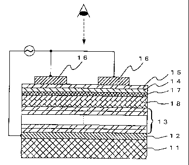
Fig. 1 is illustrative of the structure of the thin-film
EL device according to the invention. The thin-film EL device
of the invention comprises an electrically insulating substrate
11, a lower electrode layer 12 having a given pattern and a
multilayer dielectric layer stacked on the lower electrode layer,
wherein at least one lead-based dielectric layer 13 formed by
repeating the solution coating-and-firing process once or more
times and at least one non-lead, high-dielectric-constant
dielectric layer 18 are stacked together in such a way that the
uppermost surface layer of the dielectric layer is defined by
the non-lead, high-dielectric-constant dielectric layer.
Stacked on the dielectric layer are a thin-film insulator layer
17, a light-emitting layer 14, a thin-film insulator layer 15
and a transparent electrode layer 16. In this connection, the
insulator layers 17 and 15 may be dispensed with. The lower
electrode layer and upper transparent electrode layer are each
configured in a striped fashion, and are located in mutually
orthogonal directions. The lower electrode layer and upper
transparent electrode layer are respectively selected and
voltage is selectively applied to the light-emitting layer at
sites where both electrodes cross at right angles, whereby
specific pixels are allowed to emit light.
For the substrate, any desired material may be used provided
that it has electrical insulating properties and maintains given
CA 02352529 2001-07-06
-~.1-
heat-resistant strength without contaminating the lower
electrode layer and dielectric layer formed thereon.
Exemplary substratesare ceramic substratessuch as alumina
(A1203), quartz glass (Si02), magnesia (Mg0), forsterite
( 2MgO' SiOz ) , steatite (MgO' Si02 ) , mullite ( 3A1203' 2Si02) ,
beryllia ( Be0 ) , zirconia ( Zr02 ) , aluminum nitride ( A1N ) , silicon
nitride (SiN) and silicon carbide (SiC) substrates, and glass
substrates such as crystallized glass, high heat-resistance
glass and green sheet glass substrates. Enameled metal
substrates, too, may be used.
Of these substrates, particular preference is given to
crystallized glass and high heat-resistance glass substrates as
well as green sheet glass substrates on condition that they are
compatible with the firing temperature for the dielectric layer
to be formed due to their low cost, surface properties, flatness
and ease of large-area substrate fabrication.
The lower electrode layer is configured in such a way as
to have a pattern comprising a plurality of stripes . It is then
desired that the line width define the width of one pixel and
the space between lines define a non-light emission area, and
so the space between lines be reduced as much as possible.
Although depending on the end display resolution, for instance,
a line width of 200 to 500 pm and a space of about 20 um are needed.
The lower electrode layer should preferably be formed of
a material which ensures high electrical conductivity, receives
no damage during dielectric layer formation, and has a low
reactivity with respect to the dielectric layer or light-
emitting layer. Desired for such a lower electrode layer
material are noble metals such as Au, Pt, Pd, Ir and Ag, noble
metal alloys such as Au-Pd, Au-Pt, Ag-Pd and Ag-Pt, and electrode
materials composed mainly of noble metals such as Ag-Pd-Cu with
base elements added thereto, because oxidation resistance with
respect to an oxidizing atmosphere used for the firing of the
dielectric layer material can be easily obtained. Use may also
be made of oxide conductive materials such as ITO, Sn02 (Nesa
film) and Zn0-A1 or, alternatively, base metals such as Ni and
Cu provided that the firing of the dielectric layer must be
CA 02352529 2001-07-06
-12-
carried out at a partial pressure of oxygen at which these base
metals are not oxidized. The lower electrode layer may be formed
by known techniques such as sputtering, evaporation, and plating
processes.
The dielectric layer should preferably be constructed of
a material having a high dielectric constant and high dielectric
strength. Here let e1 and e2 stand for the dielectric constants
of the dielectric layer and light-emitting layer, respectively,
and dl and d2 represent the thicknesses thereof. When voltage
Vo is applied between the upper electrode layer and the lower
electrode layer, voltage V2 is then given by
V2/Vo = (e1 x d2)/(el x d2 + e2 x d1) '~' (1)
Here the specific dielectric constant and thickness of the
light-emitting layer are assumed to be e2 = 10 and d2 = 1 pm.
Then,
V2/Vo = el/(el + 10 x d1) " ~ (2)
The voltage effectively applied to the light-emitting layer
should be at least 50~, preferably at least 80~, and more
preferably at least 90~ of the applied voltage. From the
aforesaid expressions, it is thus found that:
for at least 50~, e1 Z 10 x dl ~~' (3)
for at least 80~, e1 Z 40 x dl ~~~ (4)
for at least 90~, e1 Z 90 x dl w (5)
In other words, the specific dielectric constant of the
dielectric layer should be at least 10 times , preferably at least
40 times , and more preferably at least 90 times as large as the
thickness of the dielectric layer as expressed in pm. For
instance, if the thickness of the dielectric layer is 5 um, the
specific dielectric constant thereof should be at least 50,
preferably at least 200, and more preferably at least 450.
For such a high-dielectric-constant material, various
possible materials may be used. However, preference is given
to (ferroelectric) dielectric materials containing lead as an
consistuting element because of their ease of synthesis and
low-temperature formation capability. For instance,useis made
of dielectric materials having perovskite structures such as
PbTi03 and Pb ( ZrXTil_x ) 03 , composite perovskite-relaxor
CA 02352529 2001-07-06
-13-
ferroelectric materials represented by Pb(Mgl~3Ni2~3 )03 or the like,
and tungsten bronze ferroelectric materials represented by
PbNb06 or the like. Among others, preference is given to
ferroelectric materialshaving perovskitestructuressuch as PZT,
because they have a relatively high dielectric constant and are
easily synthesized at relatively low temperatures due to the fact
that the main constituting element lead oxide has a relatively
low melting point of 890°C.
The aforesaid dielectric layer is formed by solution
coating-and-firing processes such a sol-gel process and an MOD
process. Generally, the sol-gel process refers to a film
formation process wherein a given amount of water is added to
a metal alkoxide dissolved in a solvent for hydrolysis and a
polycondensation reaction, and the resultant precursor solution
of a sol having an M-O-M bond is coated and fired on a substrate,
and the MOD (metallo-organic decomposition) process refers to
a film formation process wherein a metal salt of carboxylic acid
having an M-O bond, etc. is dissolved in an organic solvent to
prepare a precursor solution, and the obtained solution is coated
and fired on a substrate. The precursor solution herein used
is understood to mean a solution containing an intermediate
compound produced in the film formation process such as the
sol-gel or MOD process wherein the raw compound is dissolved in
a solvent.
Generally, the sol-gel and MOD processes are used in
combination, rather than used as perfectly separate processes.
For instance, when a PZT film is formed, a solution is adjusted
using lead acetate as a Pb source and alkoxides as Ti and Zr
sources . In some cases , two such sol-gel and MOD processes are
collectively called the sol-gel process. In the present
disclosure, either process is referred to as the solution
coating-and-firing process because a film is formed by coating
and firing the precursor solution on a substrate. It is here
noted that the dielectric precursor solution used herein
includes a solution wherein dielectric particles of the order
of sub-um are mixed with the precursor solution and the solution
CA 02352529 2001-07-06
-14-
coating-and-firing process used herein includes a process
wherein that solution is coated and fired on a substrate.
The solution coating-and-firing process, whether it is the
sol-gel process or the MOD process , enables a dielectric material
to be synthesized at a temperature much lower than that used for
a method making essential use of the sintering of ceramic powders
as in the case of forming a dielectric material by a thick-film
process, because the dielectric forming element is uniformly
mixed on the order of sub-dam or lower.
Taking PZT as an example, a high temperature of 900 to
1, 000° C or higher is needed for ordinary ceramic powder sintering
processes; however, if the solution coating-and-firing process
is used, it is then possible to form a film at a low temperature
of about 500 to 700° C.
Thus , the formation of the dielectric layer by the solution
coating-and-firing process makes it possible to use high
heat-resistance glass, crystallized glass, green sheet glass or
the like which could not have been used with conventional
thick-film processes in view of heat resistance.
For the synthesis of lead-based dielectric ceramics, it is
required to use the starting composition in excess of lead, as
widely known in the art . To form a uniform lead-based dielectric
material having satisfactory dielectric properties at low
temperature using such a solution coating-and-firing process,
an excess ( of the order of a few ~ to 20~ ) of the lead component
must be added to ceramics, as well known in the art.
In the case of the solution coating-and-firing process, the
larger excess lead component is needed for prevention of reduced
crystal growth due to the evaporation of the lead component during
firing and the resulting lead deficiency as well as for the
following possible reasons. Excessive lead of the lead
component forms a low-melting composition portion which
facilitates the diffusion of substance during crystal growth and
makes reactions atlowtemperature possible; reactionsoccurring
at temperatures lower than those for ordinary ceramics make an
excessive lead component likely to be more entrapped in grown
dielectric crystal grains as compared with ceramics; much more
CA 02352529 2001-07-06
-15-
lead component is needed to maintain a sufficiently excessive
lead state at each crystal growing site because the distance of
diffusion of the excessive lead component is short; and so on.
The dielectric layer made up of the lead-based dielectric
material to which the lead component is added in excess for such
reasons is characterized in that it contains , in addition to the
lead content incorporated in the crystal structure, a large
excessive lead component in the state of lead oxide.
Such an excessive lead component precipitates easily from
within the dielectric layer under thermal loads after the
formation of the dielectric layer, especially thermal loads in
a reducing atmosphere. Especially under the thermal loads in
a reducing atmosphere, metal lead is likely to occur due to the
reduction of lead oxide. If such a light-emitting layer as
mentioned later is formed directly on this dielectric layer,
there would then be a light emission luminance drops and
considerable adverse influences on long-term reliability
through the reaction of the light-emitting layer with the lead
component and contamination of metal lead ions movable into the
light-emitting layer.
In particular, the metal lead ions have high migration
capability, and behave as movable ions in the light-emitting
layer to which high electric fields are applied, producing some
considerable influences on light emission properties and, hence,
especially increased influences on long-term reliability.
Even when lead oxide is not reduced to metal lead by the
reducing atmosphere in particular, the incorporation of the lead
oxide component in the light-emitting layer causes lead oxide
to be reduced by electron impacts due to high electric fields
within the light-emitting layer with the result that the released
metal ions have an adverse influence on reliability.
In addition to the lead-based dielectric layer formed by
repeating the solution coating-and-firing process plural times,
the thin-film EL device of the invention comprises a non-lead,
high-dielectric-constant dielectric layer at least on its
uppermost surface layer.
CA 02352529 2001-07-06
-16-
This non-lead, high-dielectric-constant dielectric layer
makes it possible to reduce the diffusion of the lead component
from the lead-based dielectric layer into the light-emitting
layer and prevent the excessive lead component from having an
adverse influence on the light-emitting layer.
The influence of the addition of this non-lead dielectric
layer on the specific dielectric constant of the dielectric layer
is now explained. Here let e3 and e4 represent the specific
dielectric constants of the lead-based dielectric layer and
non-lead dielectric layer, respectively, and d3 and d4 stand for
the total thicknesses of the respective layers. Then, the
effective specific dielectric constant e5 of the entire
dielectric layer arrangement comprising the lead-based
dielectric layer and non-lead dielectric layer is given by
e5 = e3 x 1/[1 + (e3/e4) x (d4/d3)] " ' (6)
In consideration of the relations between the specific
dielectric constants of the aforesaid dielectric and light-
emitting layers and the effective voltage applied to the
light-emitting layer, the decrease in the effective specific
dielectric constant of the composite lead-based
dielectric/non-lead dielectric layer must be reduced as much as
possible. Preferably, the specific dielectric constant of the
composite layer should be at least 90~ , and especially at least
95~, of that of a single dielectric layer. From expression ( 6 ) ,
it is thus found that
for at least 90~, e3/d3 S 9 x e4/d4 ~~' (7)
for at least 95~, e3/d3 S 19 x e4/d4 '~~ (8)
For instance, if the specific dielectric constant and
thickness of the dielectric layer are assumed to be 1,000 and
8 um, respectively, then the ratio of the specific dielectric
constant and thickness of the non-lead dielectric layer should
preferably be at least 1,125, and especially at least 2,375.
Therefore, if the thickness of the non-lead dielectric layer is
assumed to be 0.2 pm and 0.4 pm, then the specific dielectric
constant should then be 225 to 475 or greater and 450 to 950 or
greater, respectively.
CA 02352529 2001-07-06
-17-
For the purpose of preventing diffusion of lead, the
thickness of the non-lead dielectric layer should preferably be
as large as possible. According to the inventor's experimental
studies, the thickness of the non-lead dielectric layer should
be preferably at least 0.2 um, and more preferably at least 0.4
um. If no problem arises in conjunction with the decrease in
the effective specific dielectric constant, then the non-lead
dielectric layer is allowed to have a much larger thickness.
Even when the thickness of the non-lead dielectric layer
is less than 0.2 pm, some effect on prevention of the diffusion
of lead may be obtained. However, any satisfactory effect on
prevention of the diffusion of lead is hardly obtained because
of minute surface defects in the lead-based dielectric layer or
the surface roughness thereof, or the local surface roughness
of the non-lead dielectric layer due to the deposition of dust
or the like ascribable to fabrication steps . This may otherwise
result in a local decrease or deterioration in the luminance of
the light-emitting layer due to the local diffusion of the lead
component.
For this reason, the non-lead dielectric layer should
preferably be as thick as possible and the specific dielectric
constant required for the non-lead dielectric layer should
evidently be preferably at least 50~ of, and more preferably
equivalent to, that of the lead-based dielectric layer.
Accordingly, and in consideration of the fact that the specific
dielectric constant necessary for the aforesaid dielectric layer
should preferably be 50 -- 200 ~ 450 or greater, the specific
dielectric constant necessary for the non-lead dielectric layer
should be at least 25, preferably at least 100, and more
preferably at least 200.
As an example, consider the case where a 0.4 um thick Si3N4
film having a specific dielectric constant of about 7 is formed
in combination with a dielectric layer having a specific
dielectric constant of 1,000 and a thickness of 8 um. From
expression (6), the effective specific dielectric constant is
then found to be 122. Even when a 0.4 um thick Taz05 film having
a specific dielectric constant of about 25 is formed, the
CA 02352529 2001-07-06
-18-
resultant effective specific dielectric constant becomes as low
as 333. As a result, the effective voltage applied to the
light-emitting layer drops largely. For this reason, the use
of such a non-lead dielectric layer causes EL device drive voltage
to become too high to obtain practical utility.
When a high-dielectric-constant material, e.g. , a Ti02 film
having a specific dielectric constant of about 80 is formed at
a thickness of 0.4 um, on the other hand, a very high effective
dielectric constant of 615 is obtained. If a substance having
a specific dielectric constant of 200 is used, then an effective
specific dielectric constant as high as 800 is obtained. The
use of a substance having a specific dielectric constant of 500
makes it possible to achieve an effective specific dielectric
constant of 910, which is substantially equivalent to that in
the absence of any non-lead dielectric layer.
Perovskite structure dielectric materials such as BaTi03 ,
SrTi03, CaTi03 and BaSn03 and their solid solutions are preferred
for non-lead, high-dielectric-constant dielectric materials
having a specific dielectric constant of 100 to 1, 000 or greater,
which exceeds about 80 that is the dielectric constant of Ti02.
By use of the perovskite structure non-lead dielectric
layer, it is thus possible to easily achieve the effect of the
invention on prevention of the diffusion of the lead component
into the light-emitting layer while the effective specific
dielectric constant decrease is minimized.
In this connection, the inventor's studies have revealed
that when such a perovskite structure non-lead dielectric layer
is used, it is of importance that its composition is such that
the ratio of A site atoms to B site atoms in the perovskite
structure is at least 1.
To be more specific, all perovskite structure non-lead
dielectric materials may crystallographically contain lead ions
at the A site. Taking a BaTi03 composition as an example,
consider the case where the starting composition for the
formation of a BaTi03 layer is such that Ba that is the A site
atom is deficient with respect to Ti that is the B site atom,
as expressed by Bal_xTi03_X. Since an excessive lead component
CA 02352529 2001-07-06
-19-
exists in the lead-based dielectric layer forming the BaTi03
layer, the Ba deficient site in the BaTi03 is easily replaced
by the excessive lead component , yielding a ( Bal_xPbx ) Ti03 layer .
When a light-emitting layer is formed on the BaTi03 layer in such
a state, no sufficient effect on prevention of the diffusion of
lead is obtained because the light-emitting layer comes in direct
contact with the lead component.
It is thus preferred that the composition of the perovskite
structure non-lead dielectric layer should be at least
stoichiometric; however, it may be shifted to an A site excess
side from the stoichiometric composition. As can be inferred
from this explanation, even when the composition of the
perovskite structure non-lead dielectric material is shifted to
an A site excess side from the stoichiometric composition, there
is a significant if remote possibility that the portion of the
non-lead dielectric layer in the vicinity of the interface with
respect to the lead-based dielectric layer may react with a part
of the lead component, because the perovskite structure non-
lead dielectric material may crystallographically be
substituted by the lead component . For this reason, the non-lead
dielectric layer should preferably have a certain or greater
thickness. According to the inventor's experimental studies,
this thickness should be 0.1 um or greater, and preferably 0.2
pm or greater.
For the formation of the non-lead dielectric layer while
its composition is under full control, it is preferable to make
use of a sputtering process or the solution coating-and-firing
process because the composition can be well controlled.
It is preferable to form the non-lead dielectric layer using
the sputtering process, because a thin film having the same
composition as the target composition can be easily formed, and
a closely packed thin film having higher density and expected
to produce a more enhanced effect on prevention of the diffusion
of the lead component can be easily formed as well.
The solution coating-and-firing process is more preferred
for the reasons that it is possible to form a dielectric layer
whose composition is more severely controlled by control of the
CA 02352529 2001-07-06
-20-
preparation ratio of the precursor solution as compared with the
sputtering process; it is possible to allow the non-lead
dielectric layer itself to have a defect correction effect that
is the feature of the solution coating-and-firing process as will
be described later; the solution coating-and-firing process is
free from any surface roughness problem due to enhanced
asperities on a substrate, which occur when a thick layer is
formed by the sputtering process on the substrate; a thick layer
can be easily formed; and the non-lead dielectric layer can be
formed without recourse to any costly film formation equipment,
viz . , with equipment and steps similar to those for the lead-based
dielectric layer.
The results of close studies by the inventor show that the
aforesaid advantages are particularly outstanding under the
following conditions.
The first condition is to provide the dielectric layer in
the form of a composite structure comprising at least one
lead-based dielectric layer and at least one non-lead, high-
dielectric-constant dielectric layer, wherein at least the
lead-based dielectric layer is formed by repeating the solution
coating-and-firing process plural times, and at least the
uppermost surface layer of the composite structure is made up
of the non-lead, high-dielectric-constant dielectric layer.
With this structure, it is possible to prevent the excessive lead
component of the lead-based dielectric layer from having an
adverse influence on the light-emitting layer, as mentioned
above.
When the lead-based dielectric layer is formed by repeating
the solution coating-and-firing process plural times,
especially at least three times, it is possible to bring the
thickness of each dielectric sub-layer at a defective site due
to dust or the like to at least 2/3 of the average thickness of
the multilayer dielectric layer. Usually, a margin of about 50%
of the predetermined applied voltage is allowed for the design
value for the dielectric strength of a dielectric layer. Thus,
a dielectric breakdown or other problem can be avoided even at
CA 02352529 2001-07-06
-21-
a locally decreased dielectric strength site resulting from the
aforesaid defects .
The second condition is to construct the non-lead
dielectric layer of a high-dielectric-constant film, and most
preferably a non-lead composition perovskite structure
dielectric material which can easily have a specific dielectric
constant of at least 100. By constructing the non-lead
dielectric layer of such a high-dielectric-constant film, it is
possible to prevent a decrease in the effective specific
dielectric constant of the composite dielectric layer due to the
inclusion of the non-lead dielectric layer. Most preferably,
a perovskite structure, non-lead, high-dielectric-constant
dielectric material isused asthe high-dielectric-constant film,
whereby the decrease in the effective specific dielectric
constant of the dielectric layer can be minimized. Especially
when the composition of the perovskite structure, non-lead,
high-dielectric-constant layer is used, it is important to shift
the composition from the stoichiometric ratio into an A site
excess side. This makes it possible to achieve a perfect effect
on prevention of the diffusion of the lead component into the
light-emitting layer.
The third condition is to form the non-lead, high-
dielectric-constant dielectric layer using the sputtering
process or the solution coating-and-firing process. With the
sputtering process, it is possible to form a high-density,
closely packed, non-lead, high-dielectric-constant dielectric
layer while its composition is easily controlled. With the
solution coating-and-firing process, it is possible to easily
form a thicker, non-lead, high-dielectric-constant dielectric
layer free from any surface asperity problem while its
composition is placed under more severe control. In addition,
the effect on correction for defects occurring on each sub-layer
due to dust or the like - which is the feature of the solution
coating-and-firing process - is also expectable during the
formation of the non-lead, high-dielectric-constant dielectric
layer. By forming both the lead-based dielectric layer and the
non-lead, high-dielectric-constant dielectric layer by
CA 02352529 2001-07-06
-22-
repeating the solution coating-and-firing process a total of
three or more times, it is thus possible to shirk a dielectric
breakdown or other problem at a locally dielectric strength
decreased site occurring through the aforesaid defects.
The fourth condition is to limit the thickness of the
multilayer dielectric layer to 4 um to 16 um inclusive. The
inventor' s studies have revealed that the particle size of dust ,
etc. occurring at processing steps in an ordinary clean room,
for the most part, is 0.1 to 2 um, especially about 1 um, and
that by bringing the average thickness of the multilayer
dielectric layer to at least 4 um and especially at least 6 pm,
it is possible to bring the dielectric strength of a defective
portion of the dielectric layer due to dust or other defects to
at least 2/3 of the average dielectric strength.
A thickness exceeding 16 um results in cost increases
because the number of repetition of the solution coating-
and-firing process becomes too large. In addition, as the
thickness of the dielectric layer increases, it is required to
increase the specific dielectric constant per se of the dielectric
layer, as can be understood from expressions (3) to (5). At a
thickness of 16 um or greater as an example, the required
dielectric constant is 160 ~ 640 - 1,440 or greater. However,
much technical difficulty is generally encountered in forming
a dielectric layer having a dielectric constant of 1,500 or
greater, using the solution coating-and-firing process. In the
invention, on the other hand, it is easy to form a defect-free
dielectric layer of high dielectric strength, and so it is
unnecessary to form a dielectric layer having a thickness
exceeding 16 pm. For these reasons, the upper limit to the
thickness is 16 pm or less, and preferably 12 um or less.
If the thickness of the dielectric layer is at least four
times as large as the thickness of the lower electrode layer,
it is also possible to make sufficient improvements in the
coverage capability for pattern edges occurring by the
patterning of the lower electrode layer and the surface flatness
of the dielectric layer.
CA 02352529 2001-07-06
-23-
The only one requirement for the stack arrangement of the
lead-based dielectric layer and non-lead, high-dielectric-
constant dielectric layer in the invention is that the uppermost
surface of the arrangement be composed of the non-lead,
high-dielectric-constant dielectric layer. Such arrangements
may be alternately stacked one upon another and the uppermost
surface of the uppermost arrangement may be composed of a non-lead,
high-dielectric-constant dielectric layer. With such a stack
arrangement, the diffusion of the excessive lead component in
the lead-based dielectric layers is effectively prevented by the
alternately stacked non-lead, high-dielectric-constant
dialectic layers, so that the effect of the uppermost non-lead,
high-dielectric-constant dielectric layer on prevention of the
diffusion of the lead component is much more enhanced. This
stack arrangement is advantageous for the non-lead, high-
dielectric-constant dielectric layer formed by the sputtering
process in particular; it is effective to avoid a noticeable
surface asperity problem associated with the sputtering process ,
which arises when a thick layer is formed thereby.
It is here appreciated that the respective sub-layers of
the lead-based dielectric layer may be formed with equal or
different thicknesses, and may be made up of identical or
different materials. The non-lead, high-dielectric-constant
dielectric layer may be made up of a plurality of materials.
For a better understanding of the advantages of the
invention, the case where the lead-based dielectric layer is
formed by repeating the solution coating-and-firing process of
the invention plural times and a dielectric layer formed by the
sputtering process, rather than the non-lead, high-
dielectric-constant dielectric layer, is provided on at least
uppermost surface of the lead-based dielectric layer is now
explained with reference to an electron microscope photograph.
Fig. 5 is an electron microscope photograph of the case where
an 8 pm thick BaTi03 thin film is formed by sputtering on a
substrate on which a 3 um thick lower electrode layer was formed
and patterned. As can be seen from Fig. 5, when the dielectric
layer is provided by sputtering, the surface of the dielectric
CA 02352529 2001-07-06
-24-
film is formed with steps enhanced on the substrate and, hence,
there are noticeable asperities and overhangs on the surface
thereof. A similar asperity phenomenon on the surface of the
dielectric layer is also found when the dielectric layer is formed
by an evaporation process, not by the sputtering process. A
functional thin film like an EL light-emitting layer cannot
possibly be formed and used on such a dielectric layer. Defects
inevitably associated with a dielectric layer formed by a
conventional process such as a sputtering process and caused by
steps on the lower electrode layer, dust or the like can be
perfectly covered up by repeating the solution coating-and-
firing process of the invention, whereby a dielectric layer
having a flattened surface can be obtained.
For the light-emitting layer material, known materials such
as the aforesaid ZnS doped with Mn may be used although the
invention is not particularly limited thereto. Among these,
SrS : Ce is particularly preferred because improved properties are
achievable. No particular limitation is imposed on the
thickness of the light-emitting layer; however, too large a
thickness leads to a driving voltage rise whereas too small a
thickness causes a light emission luminance drop. By way of
example but not by way of limitation, the light-emitting layer
should preferably have a thickness of the order of 100 to 2 , 000
nm although varying with the light-emitting material used.
The light-emitting layer may be formed by vapor phase
deposition processes, among which physical vapor phase
deposition processes such as sputtering and evaporation and
chemical vapor phase deposition processes such as CVD are
preferred. Especially when the light-emitting layer is formed
of the aforesaid SrS: Ce, it is possible to obtain a light-emitting
layer of high purity by making use of an electron beam evaporation
process in a HzS atmosphere while the substrate is held at a
temperature of 500° C to 600° C during film formation.
After the light-emitting is formed, it should preferably
be treated by heating. This heat treatment may be carried out
after the electrode, dielectric layer and light-emitting layer
are stacked on the substrate in this order or, alternatively,
CA 02352529 2001-07-06
-25-
carried out (by cap annealing) after the electrode layer,
dielectric layer, light-emitting layer and insulator layer are
stacked, optionally with an electrode layer, on the substrate
in this order. Although depending on the light-emitting layer,
the heat treatment for SrS:Ce should be carried out at a
temperature of 500° C to 600° C or higher to the firing
temperature
of the dielectric layer for 10 to 600 minutes. For the heat
treatment atmosphere, Ar is preferred.
For the formation of a light-emitting layer taking full
advantage of SrS:Ce or the like, film formation should be carried
out at a high temperature of 500°C or higher in a vacuum or
reducing atmosphere, and the high-temperature thermal treatment
step should then be carried out under atmospheric pressure. With
the prior art , problems such as the reaction of the lead component
in the dielectric layer with the light-emitting layer and the
diffusion of lead are thus unavoidable. However, the thin-film
EL device of the invention can perfectly prevent the adverse
influences of the lead component on the light-emitting layer,
and so has a great advantage over the prior art.
The light-emitting layer should preferably have a thin-
film insulator layers) formed thereon, although the insulator
layers 17 and/or 15 may be dispensed with as mentioned above.
The thin-film insulator layer should have a resistivity of at
least 108 S2 ~ cm, and preferably about 101° to 1018 S2 ~ cm, and be
preferably made up of a material having a relatively high
dielectric constant of g = ca. 3 or greater. The thin-film
insulator layer, for instance, may be made up of silicon oxide
(SiOZ), silicon nitride (SiN), tantalum oxide (TaZ05), yttrium
oxide (Y203), zirconia (Zr02), silicon oxynitride (SiON), and
alumina (A1203) . The thin-film insulator layer may be formed by
sputtering, evaporation or like processes. It is then preferred
that the thin-film insulator layer have a thickness of 50 to 1, 000
nm, and especially about 50 to 200 nm.
The transparent electrode layer may be made up of oxide
conductive materials such as ITO, SnOz (Nesa film) and Zn0-A1
of 0 . 2 um to 1 um in thickness , and formed by known techniques
such as sputtering as well as evaporation techniques.
CA 02352529 2001-07-06
-26-
While the aforesaid thin-film EL device has been described
as having a single light-emitting layer, it is appreciated that
the thin-film EL device of the invention is not limited to such
construction. For instance, a plurality of light-emitting
layers may be stacked in the thickness direction or,
alternatively, a matrix combination of different types of
light-emitting layers (pixels) may be arranged on a plane.
The thin-film EL device of the invention may be easily
identified by observation under an electron microscope. That
is, it is seen that the dielectric layer formed by the repetition
of the solution coating-and-firing process of the invention is
not only in a multilayer form unlike a dielectric layer formed
by other processes but is also different in quality therefrom.
In addition, this dielectric layer has another feature of very
excellent surface smoothness.
As already explained, the thin-film EL device of the
invention allows high-performance, high-definition displays to
be easily set up because the dielectric layer, on which the
light-emitting layer is to be stacked, is of very excellent
surface smoothness and high dielectric strength, and is free form
any defect as well, and because damage to the light-emitting layer
by the excessive lead component of the dielectric layer - which
has so far been a problem with the prior art - can be prevented
altogether. Furthermore, the thin-film EL device of the
invention is so easy to fabricate that fabrication costs can be
cut down.
EXAMPLE
The present invention is now explained more specifically
with reference to examples.
A 1 yam thick Au thin film with trace additives added thereto
was formed by sputtering on a surface polished alumina substrate
of 99.6 purity, and heat treated at 700°C for stabilization.
Using a photoetching process, this Au thin film was patterned
in a striped arrangement comprising a number of stripes having
a width of 300 um and a space of 30 um.
CA 02352529 2001-07-06
-27-
A dielectric layer, i.e. , a PZT dielectric layer was formed
on the substrate using the solution coating-and-firing process .
The dielectric layer was formed by repeating given times the
solution coating-and-firing process wherein a sol-gel solution
prepared as mentioned below was spin coated as a PZT precursor
solution on the substrate and fired at 700°C for 15 minutes.
To prepare a basic sol-gel solution, 8.49 grams of lead
acetate trihydrate and 4 .17 grams of 1, 3-propanediol were heated
under agitation for about 2 hours to obtain a transparent solution.
Apart from this, 3.70 grams of a 70 wt~ 1-propanol solution of
zirconium~normal propoxide and 1.58 grams of acetylacetone were
heated under agitation in a dry nitrogen atmosphere for 30 minutes
to obtain a solution, which was then heated under agitation for
a further 2 hours, with the addition thereto of 3.14 grams of
a 75 wt~ 2-propanol solution of
titanium~diisopropoxide~bisacetyl acetonate and 2.32 grams of
1, 3-propanediol. Two such solutions were mixed together at 80° C,
and the resultant mixture was heated under agitation for 2 hours
in a dry nitrogen atmosphere to prepare a brown transparent
solution. This solution, after held at 130° C for a few minutes
to remove by-products therefrom, was heated under agitation for
a further three hours, thereby preparing a PZT precursor
solution.
The viscosity of the sol-gel solution was regulated by
dilution with n-propanol. By control of the spin coating
conditions and the viscosity of the sol-gel solution, the
thickness of each sub-layer in the dielectric layer was regulated
to 0.7 um. The PZT layer formed under this condition contained
the lead component in an about 10~ excess of the stoichiometric
composition.
By repeating the spin coating and firing of the aforesaid
sol-gel solution as the PZT precursor solution ten times, a
lead-based dielectric layer of 7 um in thickness was formed.
This PZT film was found to have a specific dielectric constant
of 600.
For the non-lead, high-dielectric-constant dielectric
layer, a BaTi03 film was formed on the lead-based dielectric layer
CA 02352529 2001-07-06
-28-
by the solution coating-and-firing process. In addition, a
BaTi03 film, an SrTi03 film, and a Ti02 film was formed on the
lead-based dielectric layer by the sputtering process. In this
way, samples were obtained. For the purpose of comparison, a
sample was prepared without recourse of any non-lead, high-
dielectric-constant dielectric layer.
The BaTi03 thin film was formed at an Ar gas pressure of
4 Pa and a 13.56 MHz high-frequency electrode density of 2 W/cm2,
using a magnetron sputtering system wherein a BaTi03 ceramic
material was used as a target. The then film deposition rate
was about 5 nm/min. , and a thickness of 50 nm to 400 nm was obtained
by control of the sputtering time. The thus formed BaTi03 thin
film was in an amorphous state, and the heat treatment of this
film at 700°C gave a specific dielectric constant of 500. By
X-ray diffractometry, the heat-treated BaTi03 thin film was
identified to have a perovskite structure. The composition of
this BaTi03 thin film contained Ba in a 5% excess of the
stoichiometric composition.
The SrTi03 thin film was formed at an Ar gas pressure of
4 Pa and a 13.56 MHz high-frequency electrode density of 2 W/cmz,
using a magnetron sputtering system wherein an SrTi03 ceramic
material was used as a target. The then film deposition rate
was about 4 nm/min., and a thickness of 400 nm was obtained by
control of the sputtering time. The thus formed SrTi03 thin film
was in an amorphous state, and the heat treatment of this film
at 700°C gave a specific dielectric constant of 250. By X-ray
diffractometry, the SrTi03 thin film heat treated at a
temperature higher than 500° C was identified to have a perovskite
structure. The composition of this SrTi03 thin film contained
Sr in an 3% excess of the stoichiometric composition.
The Ti02 thin film was formed at an Ar gas pressure of 1
Pa and a 13.56 MHz high-frequency electrode density of 2 W/cm2,
using a magnetron sputtering system wherein a TiOz ceramic
material was used as a target. The then film deposition rate
was about 2 nm/min. , and a thickness of 400 nm was obtained by
control of the sputtering time. The heat treatment of this film
at 600°C gave a specific dielectric constant of 76.
CA 02352529 2001-07-06
-29-
The BaTi03 film by the solution coating-and-firing process
was formed by repeating given times a process wherein a sol-
gel solution prepared as mentioned below was spin coated as a
BaTi03 precursor solution on a substrate, then heated to a maximum
temperature of 700°C at an incremental heating rate of 200°C,
and finally fired at the maximum temperature for 10 minutes.
To prepare the BaTi03 precursor solution, PVP (polyvinyl
pyrrolidone) having a molecular weight of 630, 000 was completely
dissolved in 2-propanol, and acetic acid and titanium
tetraisopropoxide were added to the resulting solution under
agitation, thereby obtaining a transparent solution. A mixed
solution of pure water and barium acetate was added dropwise to
this transparent solution under agitation. While stirring was
continued in this state, the resultant solution was aged for a
given time. The composition ratio for the respective starting
materials was barium acetate: titanium
tetraisopropoxide:PVP:acetic acid:pure water:2-propanol =
1: 1:0. 5: 9: 20: 20. In this way, the BaTi03 precursor solution was
obtained.
The coating and firing of the aforesaid BaTi03 precursor
solution was carried out once, and twice, thereby obtaining a
BaTi03 dielectric layer of 0.5 um, and 1.0 pm in thickness,
respectively. This film had a specific dielectric constant of
380 and a composition in coincidence with the stoichiometric
composition.
The substrate on which the lead-based dielectric layer and
non-lead, high-dielectric-constant dielectric layer were
stacked was provided thereon with a light-emitting layer of
SrS:Ce by means of an electron beam evaporation process while
the substrate was held at a temperature of 500°C in a HzS
atmosphere for film formation. The light-emitting layer was
then heat treated at 600°C for 30 minutes in a vacuum.
Then, the light-emitting layer was successively provided
thereon with an Si3N4 thin film as an insulator layer and an ITO
thin film as an upper electrode layer by means of sputtering,
thereby obtaining a thin-film EL device. In this case, the upper
electrode layer of ITO thin film was formed according to a pattern
CA 02352529 2001-07-06
-30-
comprising stripes of 1 mm in width, using a metal mask. The
light emission properties of the obtained device structure were
measured with the application of an electric field at which the
light emission luminance was saturated at a pulse width of 50
us at 1 kHz while electrodes were led out of the lower electrode
and upper transparent electrode.
The properties to evaluate were light emission threshold
voltage, saturated luminance, and deterioration in the luminance
reached after100hour-continuouslightemission. The non-lead,
high-dielectric-constant dielectric layers in Table 1, e.g.,
SP-BaTi03 and SOL-BaTi03, are understood to mean BaTi03 formed
by the sputtering and solution coating-and-firing processes,
respectively.
CA 02352529 2001-07-06
-31-
da ~ da as da ap da as
0 o m we o m
tY~ r1 N
~ U U U U U U U U 'U
U
cCfO
~ O O O O O O O O O
U O tffO~N M O tnO N
r1 N N
a xo
a
o a~
~, 'Nro > > ~ ~ > ~ >
~-~O O u7O N d' O M v0
ri ~ 0 ~ ~1 d'd' d'd' lnd' d'
a w > ~
u~
U O ~ N d'd' ~d'~ O
''~i O O O O O O O r1
r~
E
'fl
U
cd
N
U U
O O O O O ~ E O
O U A i b b b b N N pp 0~0
+~~ PG G4G4 a7tn ~ i i
b w o a~ w w w w ~na a
a A + v~ ~n~n ~n~n ~ can
~ a~ ~
o .~ o cd
z x v a
N
x
U I~t~ I~I~ I~l~ I~l~ t~
E
r-I
'J
td
~n S~ N
G
~ N N N N N N N N N ~
PaG~ PaPa W ~ Pa~L ~ p
.r1
~
a a a ..
..
*
*
* * * * * * * *
* * * * * * * * *
'-.i N c~ m ~o ~ m a
CA 02352529 2001-07-06
-32-
As a result, the comparative example free from the non-
lead, high-dielectric-constant dielectric layer showed a
luminance deterioration of as large as 50~, and the samples
containing the BaTi03 layer formed by the sputtering process
according to the invention had a luminance reached of about 1, 200
cd at a thickness of 0.2 um or greater and a light emission
threshold voltage of about 140 V, with only limited luminance
deterioration. At less than 0.1 pm, on the other hand, the light
emission threshold voltage increased with a decreasing luminance
reached, resulting in further considerable luminance
deterioration. The SrTi03 layer gave much the same properties
as in the case of the BaTi03 layer having the same thickness,
although there was a slight light emission threshold voltage
increase. The BaTi03 layer formed by the solution coating-
and-firing process, too, gave much the same properties as in the
case of the dielectric layers obtained by sputtering, although
there was a slight light emission threshold increase.
The Ti02 film was higher in threshold voltage and lower in
luminance than the BaTi03 film having the same thickness, with
some remarkable luminance deterioration.
In the comparative structure composed only of PZT, there
were light emission threshold increases as well as luminance
decreases with considerable luminance deterioration. In
addition, a dielectric breakdown was often found at an applied
voltage in the vicinity of the luminance reached.
As can be seen from these results, the structure using the
non-lead, high-dielectric-constant perovskite layer as the
non-lead, high-dielectric constant layer started to show its
effect at a thickness of at least 0.1 um, and exhibited a
remarkable light emission luminance increase, a significant
threshold voltage drop, and reliability improvements especially
at 0.2 um or greater.
This reveals that the diffusion of the lead component in
the lead-based dielectric layer into the light-emitting layer
is effectively prevented.
The TiOz layer was lower in saturated luminance , higher in
light emission threshold voltage and more significant in
CA 02352529 2001-07-06
-33-
luminance deterioration than the perovskite layer, although it
was found to have a certain effect as a reaction preventive layer.
This is believed to be probably because the TiOz film was partly
placed in a PbTi03 state through the reaction with the excessive
lead in the PZT layer, and so could not perfectly function as
a reaction preventive layer.
ADVANTAGES OF THE INVENTION
The advantages of the invention can be understood from the
foregoing. According to the invention, the defects occurring
in the dielectric layer - which are one problem associated with
the prior art - can be eliminated. In particular, a solution
can be provided to problems in conjunction with the light emission
luminance drops, luminance variations, and changes of light
emission luminance with time of a thin-film EL device wherein
the multilayer dielectric layer is constructed using the
solution coating-and-firing process. It is thus possible to
provide, without incurring any added cost, a thin-film EL device
capable of presenting displays of high quality, and a process
for the fabrication of the same.