Note: Descriptions are shown in the official language in which they were submitted.
CA 02353422 2003-03-14
- 1 -
HIGH FREQUENCY DC TO AC INVERTER
TECFINICAI~ FIELD
This invention relates to power supplies for
electronic equipment and, in particular, to inverters for
generating high frequency sinusoidal AC voltages for
electronics equipment used in telecommunications and
computer systems. Typical examples of potential use are in
personal computers, servers, routers, network processors,
and opto-electronic equipment.
BACKGROUND OF THE INVENTION
Segments of th.e personal computer (PC) industry have
dramatically changed during the last decade. The future is
even more challenging. A dramatic increase in the
processor speeds of PCs has required an overwhelming
increase in current and associated dynamics (very high slew
rate). This already challenging technical requirement is
further complicated by a need for voltage reduction,
potentially to sub-volt levels.
In the past, there was virtually no challenge in
powering computers. A multiple output, very slow power
supply called a "Silver Box (SB)" was adapted to meet the
requirements of every power demand. However, as silicon
development progressed, multiple voltages of less than 3.3V
were required. Voltage Regulator Modules (VRMs) on the
processor Mother Board (MB) were a logical solution to that
problem. Today, the number of VRMs required on the Mother
CA 02353422 2001-07-23
- 2 -
Board is increasing. In addition to the VRMs, a large
number of de-coupling capacitors are required in proximity
of the processor to meet the requirements of very high slew
rate of the current. This has resulted in a rapid increase
in the cost, as well as a large reduction in overall
efficiency, of the power delivery system.
A number of options for improving this situation
have been explored. For example, Advanced Voltage
Regulator Module (AVRM) offers the capability to supply
high di/dt and high current, however, at increased cost,
and with low efficiency and moderately high capacity of the
de-coupling capacitors. Replacing low voltage DC
distribution with higher DC voltage, :>uch as 48V, is more
promising but has a drawback of higher cost. Recently a
novel High Frequency Alternating Current (HFAC) power
delivery architecture has been proposed for powering the
future generation PCs in reference entitled, "PC Platform
Power Distribution System: Past supplication, Today's
Challenge and Future Direction " published in the
conference proceedings of International Telecommunications
Energy Conference, Copenhagen, Denmark, June 1999 by
J.Drobnik, L.Huang, P.Jain and R.Steigerwald. In the HFAC
architecture, the system power supply (silver box)
generates high frequency and high voltage. The HFAC is
then fed to an individual AC-DC converter (ACVRM) and
converted into DC of specific parameters at the point of
use.
CA 02353422 2001-07-23
- 3 -
HFAC is conceptually the simplest architecture
proposed to date, which deals with all of the power
delivery issues defined above. This includes elimination
of duplicated power conversions, and active energy steering
without additional components.
The key to successful implemE:ntation of an HFAC
power delivery system resides in the two stages of power
conversion namely; DC to AC high frequency conversion stage
and the stage that converts high frequency AC to DC.
FIG. 1 shows a block diagram of a conventional DC to
high frequency AC inverter 100. The inverter 100 includes
a full-bridge inverter 104 having an input 104A for
receiving a DC input voltage 102 and providing an
output 104B. The output 104B is con:~ected at 106 to an
input 108A of a resonant circuit 108. An output 108B of
the resonant circuit 108 provides a high frequency AC
output voltage 110. The AC output voltage 110 is fed
back 112 to an input 114A of a phase-shift modulation
circuit 114. The modulation circuit provides four
outputs 114B connected at 116 to four inputs 118A of a gate
drive circuit 118. The gate drive circuit 118 has four
outputs 118B connected at 120 to four inputs 104C of the
inverter 104.
A number of power circuit configurations to
implement the full-bridge inverter and resonant circuit of
FIG. 1 are possible but the circuits as shown in FIGS. 2A
CA 02353422 2001-07-23
- 4 -
and B are the circuits most commonly used in these
implementations.
FIG. 2A shows the full-bridge inverter 104 and the
resonant circuit 108 sections of a conventional
inverter 200 which was described in 'A 20 kHz Hybrid
Resonant Power Source for the Space Station', IEEE Trans.
on Aerospace and Electronics Systems, vol. 25, No. 4, July
1989, 491-496 by P.Jain & M.Tanju. The full-bridge
inverter 104 includes a first switch 202, a second
switch 204, a third switch 206, and a fourth switch 208.
Each switch 202,204,206,208 is preferably an N-channel
field-effect transistor (FET). The .resonant circuit 108
includes a series resonant circuit 210, a parallel resonant
circuit 212, and a transformer 214.
The full-bridge inverter 104 produces a quasi-square
voltage at its output 106, which is controlled using a
phase-shift modulation circuit 114 (FIG. 1) commonly used
in such applications. Both the series 210 and parallel 212
resonant circuits are tuned to an operating frequency of
the inverter. Although the resonant circuit 108 produces a
regulated sinusoidal voltage at its; output 110, this
inverter 200 does not provide zero-voltage switching
conditions for at least two of the four
switches 202,204,206,208, which results in higher switching
losses at higher operating frequencies. Therefore, the
operation of this circuit is limited to lower operating
frequencies.
CA 02353422 2001-07-23
- 5 -
FIG. 2B shows the full-bridge inverter 104 and the
resonant circuit 108 sections of a conventional
inverter 250 which was described in 'Constant frequency
resonant DC/DC converter', US Patent ~' 5,157,593, Oct. 20,
1992 by P.Jain. The full-bridge inverter 104 is identical
to the one shown in FIG. 2A. The resonant circuit 108
includes a series resonant circuit 210,. a parallel resonant
circuit 252, and a transformer 214.
The full-bridge circuit 104 produces a quasi-square
voltage at its output 106, which is controlled using a
phase-shift modulation circuit 114 (FIG. 1) commonly used
in such applications. In this configuration; the series
resonant circuit 210 is tuned to an operating frequency of
the inverter 250 while the parallel ciz:cuit 252 is tuned at
a frequency, which is lower than the operating frequency.
Although the resonant circuit 108 produces a regulated
sinusoidal voltage at its output 110 and provides zero-
voltage switching conditions for' all the four
switches 202,204,206,208, the de-tuning of the parallel
branch 252 requires the series resonant components 210 and
the output transformer 214 to have higher maximum ratings
and hence be more expensive.
Another fundamental problem that limits the
operation of the inverter circuits of FIGS. 2A and B at
higher operating frequencies is gate circuit losses of the
FETs 202,204,206,208 used in the full-bridge circuit 104.
FIG. 3 shows a graph 300 of typical gating signals Al 302,
A2 304, Bl 306, and B2 308 produced by the phase-shift
CA 02353422 2001-07-23
- 6 -
circuit 114. FIG. 4 shows a graph 400 of gate voltage
(VgA1) 402, gate current (igAl) 404,. instantaneous gate
power (pgA1) 406, and average gate power (PgAl) 408 for a
gate 202A of the first FET switch 202. This graph 400
clearly shows that when a rectangular voltage pulse 402 is
applied to the gate 202A of the FET 202, which has a
capacitance, a pulsating current 404 is drawn from. this
voltage. This causes the power loos 406 in the gate
circuit, which is approximately given by Cg*Vg2*f 408 (where
Cg is gate capacitance; Vg is gate vo:Ltage; and, f is the
operating frequency). At higher frequE:ncy, the gate losses
are prohibitively high, which limits the operation of
inverter circuits of FIG. 2A and B at very high frequency.
It is clear from the above discussion that the
conventional approaches to converting DC to high frequency
AC have low conversion efficiency due to high switching
losses.
There therefore exists a need for an inverter
topology, which is capable of operating at substantially
higher frequencies and has no, or very small, switching
losses, including gate circuit losses.
SUN~ARY OF THE INVENTION
It is therefore an object of the invention to
provide a DC/AC inverter, which forms a high frequency
sinusoidal AC source.
CA 02353422 2001-07-23
-
The invention therefore provides a high-frequency
resonant sine wave DC to AC inverter suitable for use in a
personal computer (PC) power supply, which includes a full-
bridge inverter, a resonant circuit, a phase shift
modulation circuit, and a resonant gate driver. The
resonant gate driver provides sinusoidal gate drive signals
to the full-bridge inverter enabling highly efficient
operation on the inverter.
The invention further provides a method of driving
an inverter to convert direct current (DC) to alternating
current (AC), comprising a step of receiving square wave
gating signals at a resonant gate driver and modifying the
square wave gating signals to form sinusoidal gating
signals for driving the inverter.
BRIEF DESCRIPTION OF THE DRAWINGS
Further features and advantages of the present
invention will become apparent from th.e following detailed
description, taken in combination with the appended
drawings; in which:
FIG. 1 is a block diagram of a conventional AC to
high frequency AC voltage inverter;
FIGS. 2A and 2B are circuit diagrams of conventional
full-bridge inverter and resonant circuits;
FIG. 3 is a graph of gaping signals of a
conventional DC to AC inverter;
CA 02353422 2001-07-23
_ g _
FIG. 4 is a graph of gate voltage, current,
instantaneous power, and average power of a gate of the
inverter of FIG. 2A;
FIG. 5 is a block diagram of an AC to DC inverter in
accordance with the present invention;
FIG. 6 is a graph of gating signals used in the AC
to DC inverter of FIG. 5;
FIG. 7 is a graph of gated voltage, current,
instantaneous power and average power of the inverter of
FIG. 5;
FIG. 8 is a schematic diagram of a resonant gate
drive circuit of FIG. 5;
FIG. 9 is a graph of voltage and current waveforms
of the resonant gate drive circuit of FIG. 8;
FIGS. 10 to 12 are schematic diagrams of alternative
embodiments the resonant gate drive cir~~uit of FIG. 8;
FIG. 13A is a schematic diagram of the full-bridge
inverter and resonant circuit of FIG. 5;
FIG. 13B is a graph of operating waveforms of the
full-bridge inverter and resonant circuit of FIG. 13A; and
FIGS. 14 to 18 are schematic diagrams of alternative
embodiments full-bridge inverter and resonant circuit of
FIG. 5.
CA 02353422 2001-07-23
- 9 -
It will be noted that throughout the appended
drawings, like features are identified by like reference
numerals.
DETAINED DESCRIPTION OF THE PREFERRED E:N~ODIMENTS
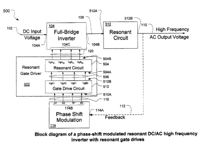
A block diagram 500 of a preferred embodiment of the
present invention is shown in FLG. 5. This block
diagram 500 is identical the block diagram 100 shown in
FIG. 1 except that the gate drive circuit 118 has been
replaced by a resonant gate drive circuit 502, and the
resonant circuit 108 has been replaced by an improved
resonant circuit 512 which provides loss-less switching of
all the FETs 202,.204,206,208 of the full-bridge
inverter 104 without excessive rating of components in the
resonant circuit 512. These two aspects of the present
invention are described below.
RESONANT GATE DRIVER
The resonant gate driver 502 as shown in FIG. 5
consists of a conventional gate drivE: circuit 510 and a
resonant circuit 504. The gate drive circuit 510 has four
inputs 510A that are connected 1.16 to the gating
signals 114B (Al, A2, B1, B2) from the phase-shift
modulation circuit 114. The gate drive circuit 510
generates rectangular voltage pulsea 510B (VgAl 602,
VgA2 604, VgBl 606, VgB2 608 in FIG. 6) that are
connected 506 respectively to four :inputs 504A of the
resonant circuit 504. The resonant circuit 504 produces
four sinusoidal voltage signals 504B (VgARl 610, VgAR2 612,
CA 02353422 2001-07-23
- 10 -
VgBRl 614, VgBR2 616 in FIG. 6) that are connected 120
respectively to the four inputs 104C of the full-bridge
inverter circuit 104.
Now referring to the graphs 700 in FIG. 7, a brief
description of the operation of the resonant gate drive 502
with respect to gate circuit losses is given here. For
simplicity only gating signals for one gate are shown in
FIG. 7. Let us assume that the sinusoidal voltage 702
(VgARl) is produced by the resonant gage circuit 502. This
voltage 702, when applied at the gate A1, produces a
sinusoidal current igAR1 at its output. Since the
gate 202A of the first FET switch S1 202 is capacitive,
current igARl 704 is also sinusoidal but. has a leading angle
of 90° with respect to voltage VgARl 702. As a result an
instantaneous power pgAR1 706, which i~> sinusoidal at twice
the frequency of the gate voltage 702, is drawn from the
resonant gate drive circuit 502. The instantaneous power
pgARl 706 has a zero average component (PgARl=0). This means
the resonant gate circuit driver 502 results in a loss-less
drive. (In actual practice, the azTerage power is not
ideally zero but has a small value due to the resistance
associated with the components of the resonant gate driver
circuit 510. But this average power loss is significantly
smaller than the Cg Vg2 f losses of th.e conventional drive
circuit 118.)
A resonant gate drive circuit 800 in accordance with
the present invention is shown in FI(.;. 8. This circuit
includes a gate driver 508; a series resonant circuit 802
CA 02353422 2001-07-23
- 11 -
comprising a series inductor 802A having a value Lsg and a
series capacitor 802B having a value Csg; and a gate drive
transformer 804 (Tg) having a primary winding 806 with N1
turns, a first secondary winding 808, and a second
secondary winding 810 each having N2 turns. A parallel
resonant circuit 812,814 comprising a parallel
inductor 812A,814A having a value Lg and a gate
capacitor 812B,8148 having a value Cg. The series 802 and
parallel 812,814 branches are tuned to a frequency of
operation of the gate driver 508. Now let us briefly
explain the operation of the circuit 8C10 of FIG. 8 with the
help of waveforms 900 as shown in FIG. 9.
After receiving the signals 11i5 A1 and A2 from the
phase-shift modulator 114 (PSM) on its input 508A, the gate
driver 508 generates a square-wave voltage 902 VgA at its
output 5088, the square-wave voltage 902 when applied at
the series combination of the series resonant circuit 802
and primary winding 806 of the transformer 804 produces a
sinusoidal voltage across the primary winding 806 of the
transformer 804. Since the parallel branch 812 is tuned to
the operating frequency of the driver 508, the application
of the sinusoidal voltage across the parallel resonant
circuit 812 produces two sinusoidal currents, iCg1 906
through the capacitor 812A and iLg1 908 through the
inductor 8128. Both the currents 906,908 have the same
magnitude but 180" phase difference. Similarly, the
application of the sinusoidal voltage across the parallel
resonant circuit 814 produces two sinusoidal currents,
CA 02353422 2003-03-14
4
- 12 -
iCg2 912 through the capacitor 814B and iLg2 914 through
the inductor 814A. Again, both the currents 912,914 have
the same magnitude but 180° phase difference. The resultant
currents igl 910 and ig2 916 at the secondary
windings 808,810 are, therefore, zero. This means the
current drawn from the driver circuit 508 is also zero.
The above description reveals the following two
characteristics of the resonant gate driver 502: (1) the
average power drawn from the resonant gate drive
circuit 502 is zero, and (2) instantaneous current supplied
by the gate driver 508 is zero. However, in actual
practice, both the average power and current supplied by
the driver 508 are not zero but have small values due to
resistance associated with components of the resonant gate
driver circuit 502. An identical resonant gate drive
circuit 800 as shown in FIG. 8 is used for driving
gates 204A,206A of the second switch 204 and third
switch 206 of the full-bridge inverter 104 with the
exception that the signals B1 and B2 are used as the input
signals 116 instead of A1 and A2.
FIG. 10 shows another embodiment of the resonant
gate driver 1000 in accordance with the present invention
in which a common parallel inductor 1002 having a value Lg
is connected across the primary winding 806 of the
transformer 804 and the inductors 812A,814A across the
secondary windings 808,810 are removed.
CA 02353422 2001-07-23
- 13 -
FIG. 11 shows another embodiment of the resonant
gate driver 1100 in accordance with the present invention
in which the parallel inductor 1002 of FIG. 10 is an
integral part of the transformer 804.
FIG. 12 shows another embodiment of the resonant
gate driver 1200 in accordance with the present invention
in which both the series 802A and parallel inductor 1002 of
FIG. 10 are integral parts of the transformer 804.
RESONANT INVERTER
A DC/AC inverter in accordance with the invention is
shown in FIG. 13A and comprises a full-bridge inverter 104
comprising four switches 202,204,206,208, a commutation
inductor 1310A having a value Lc, a blocking
capacitor 1310B having a value Cb, a high frequency
transformer 214, a series resonant circuit 210 comprising a
series inductor 210A having a values Ls and a series
capacitor 210B having a value Cs, and a parallel resonant
circuit 212 comprising a parallel inductor 212A having a
value Lp and a parallel capacitor 212B zaving a value Cp.
The full-bridge inverter 104 produces a quasi-square
voltage at its output terminals. The commutation inductor
Lc provides a zero voltage switching condition for the
inverter switches in conjunction with the parallel
capacitors 1302,1304,1306,1308 those are connected across
the switches. The transformer T is used to match the
output voltage level with the input voltage of the full-
bridge. The components Ls and Cs of the series resonant
CA 02353422 2001-07-23
- 14 -
circuit and the components Lp and Cp of the parallel
resonant circuit are tuned at the operating frequency of
the full-bridge inverter. Both the series and resonant
circuits provide filtering, for the harmonics contained in
the quasi-square wave of the full-bridge inverter, and
produce a sinusoidal voltage output across the parallel
resonant circuit. Capacitor Cb is used to prevent the
saturation of the commutation inductor Lc.
A detailed description of the resonant inverter 1300
of FIG. 13A in conjunction with the operating waveforms
1350 as shown in FIG. 13B is now given.. In operation when
the resonant gate drive signals VgARl, VgAR2, VgBRl, VgBR2 are
applied at the gates of switches 2 02, 204, 206, 208
respectively, a near quasi-square voltage waveform VAB 1362
is produced at the output 106 of the full-bridge
inverter 104. Since both the series 210 and parallel 212
resonant branches are tuned at the operating frequency of
the inverter 1300, a near sinusoidal current is 1368 through
the series branch 210, a near sinusoidal voltage Vp 1366
across the parallel branch 212, and a trapezoidal current
ILK 1370 through the commutation inductor 1310A are
established: For one cycle of operation of the
inverter 1300, the operation of the inverter 1300 is given
below.
At time t - 0, only gate voltage VgBR2 1360 at the
gate of the second switch 204 is above the gate threshold
voltage VGth 1356, which makes the second switch 204
continuously conduct. At the same timE: the net current iAB
CA 02353422 2001-07-23
- 15 -
(is+ILC) is negative, which is forcing diode 1322 to
conduct.
At t=t1, the gate voltage VgBR2 1360 falls below the
threshold voltage VGth, the second switch 204 starts to
turn-off and the negative current iAB starts to charge the
second capacitor 1304 and discharge the third
capacitor 1306. By selecting the proper value of the
second capacitor 1304, the rate of rise of voltage across
the second switch 204 can be controlled in such a way that
the current flowing through the second switch 204 falls to
zero before the voltage across the second switch 204 rises
substantially. This results in near loss-less turn-off for
the second switch 204.
At t=t2, the second capacitor 1304 has charged to
the level of input voltage Vi and the third capacitor 1306
has discharged to zero. The negative current iAB (is+ILC)
now forces the third diode 1326 to conduct.
At t=t3, the gate voltage VgARl 1352 rises above the
gate threshold voltage VGth 1356, the first switch 202 now
starts to conduct. It should be noted that the first
switch 202 turns-on under zero voltage as the first
diode 1322 across it was conducting prior to the turn-on.
At t=t5, the gate voltage VgBRl 1358 rises above the
gate threshold voltage VGth 1356, the third switch 20~ now
starts to conduct. It should be noted that the third
switch 206 turns-on under zero voltage as the third
diode 1326 across it was conducting prior to the turn-on.
CA 02353422 2001-07-23
- 16 -
At t=t6, the gate voltage VgARl 1352 falls below the
threshold voltage VGth 1356, the first switch 202 starts to
turn-off and the positive current iAB starts to charge the
first capacitor 1302 and discharge the fourth
capacitor 1308. By selecting the proper value of the first
capacitor 1302, the rate of rise of voltage across the
first switch 202 can be controlled in such a way that the
current flowing through the first switch 202 falls to zero
before the voltage across the first switch 202 rises
substantially. This results in near loss-less turn-off for
the first switch 202.
At t=t7, the first capacitor 13102 has charged to the
level of input voltage Vi and the fourth capacitor 1308 has
discharged to zero. The positive current iAB (is+ILC) now
forces the fourth diode 1328 to conduct.
At time t t8, only gate voltage VgBRl 1358 at the
gate of the third switch 206 is above the gate threshold
voltage VGth, which makes the third sw__tch 206 continuously
conduct. At the same time the net current iAB (is+ILC) is
positive, which is forcing the fourth diode 1328 to
conduct.
At t=t9, the gate voltage VgBR1 1358 falls below the
threshold voltage VGth 1356, the third switch 206 starts to
turn-off and the positive current iAB starts to charge the
third capacitor 1306 and discharge the second
capacitor 1304. By selecting the proper value of the third
capacitor 1306, the rate of rise of voltage across the
CA 02353422 2001-07-23
- 17 -
third switch 206 can be controlled in such a way that the
current flowing through the third switch 206 falls to zero
before the voltage across the third switch 206 rises
substantially. This results in near loss-less turn-off for
the third switch 206.
At t=t10, the third capacitor 1306 has charged to
the level of input voltage Vi and the second capacitor 1304
has discharged to zero. The positive current iAB (is+ILC)
now forces the second diode 1324 to conduct.
At t=t11, the gate voltage VgAR2 1354 rises above
the gate threshold Voltage VGth 1356, t:he fourth switch 208
now starts to conduct. It should be noted that the fourth
switch 208 turns-on under zero voltage as the fourth
diode 1328 across it was conducting prior to the turn-on.
At t=t12, the gate voltage VgBR2 rises above the
gate threshold voltage VGth, the second switch 204 now
starts to conduct. It should be noted that the second
switch 204 turns-on unde r zero voltage as the second
diode 1304 across it was conducting prior to the turn-on.
At t=t13, the gate voltage VgAR2 falls below the
threshold voltage VGth, the fourth switch 208 starts to
turn-off and the negative current iAB starts to charge the
fourth capacitor 1308 and discharge the first
capacitor 1302. By selecting the proper value of the
fourth capacitor 1308, the rate of rice of voltage across
the fourth switch 208 can be controlled in such a way that
the current flowing through the fourth switch 208 falls to
CA 02353422 2001-07-23
- 18 -
zero before the voltage across the fourth switch 208 .rises
substantially. This results in near loss-less turn-off for
the fourth switch 208.
At t=t14, the fourth capacitor 1308 has charged to
the level of input voltage Vi and the capacitor 1302 has
discharged to zero. The negative current iAB (is+ILC) now
forces the first diode 1322 to conduct.
At t=t15, a new cycle begins and the operation of
the inverter 104 as described above repeats.
From the above description, it is clear that the
switches of the inverter 104 are turned-on and turned-off
with near zero switching losses.
Controlling the phase shift (~) of the full-bridge
inverter 104 controls the high frequency sinusoidal output
voltage.
FIG. 14 shows another embocLiment 1400 of the
resonant inverter 500 OF FIG. 5 in which the parallel
resonant circuit 1402 of the reson<~nt circuit 512 is
connected across the secondary winding of the
transformer 214.
FIG. 15 shows another embodiment of the resonant
inverter 500 of FIG. 5 in which both the series 1502 and
the parallel resonant 1402 circuits of the resonant
circuit 512 are connected across the .secondary winding of
the transformer 214.
CA 02353422 2001-07-23
- 19 -
FIG. 16 shows another embodiment of the resonant
inverter 500 of FIG. 5 in which the paralle l resonant
inductor of the resonant circuit 512 i:> an integral part of
the transformer 214.
FIG. 17 shows another embodiment of the resonant
inverter 500 of FIG. 5 in which the series resonant
inductor of the resonant circuit 512 i:> an integral part of
the transformer 214.
FIG. 18 shows another embodiment of the resonant
inverter 500 of FIG. 5 in which both the series and the
parallel resonant inductors of the resonant circuit 512 are
the integral parts of the transformer 2.14.
PROTOTYPE INVERTER SYSTEM
A prototype of high frequency resonant inverter
system of FIG. 15 was built to verify t;he performance. The
inverter system is used to produce a 1 MHz,
sinusoidal 28Vrms, and 240 volt-ampere output power from an
input voltage of 400 V DC. The following parameters are
used for the power circuit: Cb - luF' 1310B, Lc - 76 uH
1310A, transformer 214 turns ratio (N1/N2 - 35/3),
Ls = 1 uH 1502A, Cs - 25 nF 1502B, hp - 0.43 uH 1402A,
Cp = 59 nF 1402B, the switches 1302,1304,1306,1308 are
IRF 840. The following parameters are used for the
resonant gate driver 800 of FIG. 8: Lsg - 25 uH 802A,
Csg = 1 nF 802B, turns ratio for the gate transformer 804
(N1/N2 - 10/10), Lg - 18 uH 812A,814A, and Cg - 1.3 nF
812B,814B. The output voltage had lc>wer than 1.5% total
CA 02353422 2001-07-23
- 20 -
harmonic distortion, better than to voltage regulation and
over 96o efficiency including the gate circuit.
The invention therefore provides an AC to DC
inverter capable of operating at high frequencies and has
very small switching losses.
The embodiments) of the invention described above
is(are) intended to be exemplary only. The scope of the
invention is therefore intended to be 1_imited solely by the
scope of the appended claims.