Note: Descriptions are shown in the official language in which they were submitted.
CA 02353654 2001-07-24
R Antosik 2-1-2-6-1 1
CIRCUITRY FOR MIXED-RATE OPTICAL COMMUMCATION NETWORKS
BACKGROUND OF THE INVENTION
Field of the Invention
The present invention relates to optical communications, and, in particular,
to nodes for
optical communication networks that support provisioning of optical signals.
Description of the Related Art
A typical optical communication network conforming to the Synchronous Optical
Network
(SONET) standard, comprises a set of nodes interconnected by fiber optical
links. When the
optical communication network is based on dense wavelength division
multiplexiiig (DWDM),
each optical fiber may simultaneously carry a number of different optical
signals, where each
different optical signal is transmitted at a different wavelength. In general,
the different optical
signals transmitted over a single optical fiber may have different data rates.
For example, some of
the optical signals may be OC3 signals having a data rate of 155
megabits/second (Mb/s), while
other optical signals may be OC 12 signals having a data rate of 622 Mb/s, and
still other optical
signals may be OC48 signals having a data rate of 2.5 gigabits/second (Gb/s).
In conventional SONET-based optical communication networks, each node is
configured
with circuitry designed to provision optical signals for communication with
other nodes over their
corresponding interconnecting optical links. In general, provisioning of
optical signals refers to one
or more of (1) adding a new optical signal to the communications, (2) deleting
an existing (i.e., live)
optical signal, (3) increasing the data rate of an existing optical signal
(referred to as a "rate-
upgrade"), and (4) decreasing the data rate of an existing optical signal
(referred to as a"rate-
downgrade"). In conventional nodes for SONET-based optical communication
networks, different
circuit boards are provided for the different optical signal data rates. For
example, a particular
node may have one or more circuit boards designed to handle only OC3 signals,
one or more other
circuit boards designed to handle only OC 12 signals, and one or more
additional circuit boards
designed to handle only OC48 signals.
A typical node for a SONET-based DWDM optical communication network that uses,
for
example, 40 different wavelengths per fiber may be configured with different
numbers of OC3,
OC 12, and OC48 circuit boards that, taken together, are able to provision up
to 40 different
CA 02353654 2001-07-24
R Antosik 2-1-2-6-1 2
customer signals for communication over a given optical fiber with another
node. In theory, each
DWDM wavelength is able to support the highest bandwidth signal (e.g., OC48).
In this example,
wavelengths that are assigned OC3 or OC 12 optical signals are underutilized
in terms of their
available data bandwidth.
SUMMARY OF THE INVENTION
The present invention is directed to circuitry for nodes in optical
communication networks,
such as SONET-based DWDM optical communication networks, that enables more
efficient use of
available data bandwidth. In particular, according to certain embodiments of
the present invention,
a single circuit board for a node is capable of packing a number of different
outgoing customer
signals (e.g., OC3/OC 12-rate signals) into a single outgoing optimum-rate
optical signal (e.g.,
OC48 optical signal) for transmission at a particular wavelength over an
optical fiber to another
node. The circuit board is also capable of unpacking a number of different
incoming customer
signals from a single incoming optimum-rate optical signal received from the
other node over the
same or a different optical fiber. Moreover, those different outgoing and
incoming customer
signals may have different data rates (e.g., both 0C3-rate and OC12-rate
signals packed into a
single OC48 optical signal).
As an example, in one embodiment of the present invention for a DWDM optical
communication network that uses 40 different wavelengths per optical fiber,
where each
wavelength can support a different OC48 optical signal, each circuit board in
each node of the
network is capable of (1) packing up to eight different OC3/OC12-rate outgoing
customer signals
into a single outgoing OC48 optical signal transmitted at one of the 40 DWDM
wavelengths and
(2) unpacking up to eight different OC3/OC 12-rate incoming customer signals
from a single
incoming OC48 optical signal transmitted at the same DWDM wavelength. Each
node can be
configured with 40 such circuit boards for each pair of outgoing and incoming
optical fibers (or
each optical fiber in the case of bi-directional communications on one fiber),
with each circuit board
handling a different pair of outgoing and incoming composite OC48 optical
signals, each one sent
on one of the 40 DWDM wavelengths. Such an embodiment is therefore able to
support up to 320
different pairs of outgoing and incoming customer signals per pair of optical
fibers, as opposed to
the prior art limit of only 40 different pairs of customer signals per pair of
optical fibers.
CA 02353654 2001-07-24
R Antosik 2-1-2-6-1 3
In certain embodiments, the present invention relates to the field of optical
networking
using DWDM or time division multiplexing (TDM) technology and SONET/SDH
(Synchronous
Digital Hierarchy) mixed-rate muxing and demuxing of OC3/OC12 optical signals
to/from an
OC48 DWDM optical signal to increase efficiency of use of network capacity.
The invention
addresses the complexity problem of off-line and in-line provisioning to
add/delete/rate-upgrade/rate-downgrade the mixed-rate signals, while reducing
service interruptions
of live signals. The invention serves the purpose of simplifying the above-
mentioned provisioning
with an algorithm-based, automatic assignment of the STS3 time slots in OC48
frames to the
provisioned mixed-rate signals and by automatic transmission and execution of
the port number to
STS3 time slot map in both muxing and demuxing nodes.
In the prior art, muxing and demuxing OC3/OC 12 optical signals requires
manual mapping
of the STS3 time slots to the signals. There is no transmission of the map
between the muxing and
the demuxing nodes. The disadvantage of the prior art is that each
addition/deletion/rate-upgrade/
rate-downgrade of an OC3/OC 12 signal requires retrieval of the existing time
slot assignment map
and manual re-assignment of the STS3 time slots in both muxing and demuxing
nodes. In the case
of an OC3-to-OC 12 rate-upgrade or addition of a new OC 12 signal, the
provisioning may require a
re-map of existing signals to new STS3 time slots, which may result in failing
those signals for a
relatively long time due to lack of synchronization between muxing and
demuxing nodes. Manual
mapping of the STS3 time slots is time consuming and prone to data entry
errors. It may be
acceptable in applications when signals are provisioned only once in their
lifetime. In
TDM/DWDM networks, however, the network provider is interested in a frequent
re-provisioning
of the network-muxed OC3/OC 12 signals to satisfy changing needs for bit-rate
and changing
owners of the signals.
In one embodiment, the present invention is a first node for an optical
communication
network, the first node having circuitry comprising at least one of a mux and
a demux. When the
circuitry comprises a mux, (1) the mux is configured to combine two or more
incoming electrical
signals into an outgoing electrical signal, wherein (a) at least one incoming
electrical signal has a
first frame format at a first data rate; (b) at least one other incoming
electrical signal has a second
frame format at a second data rate greater than the first data rate; and (c)
the outgoing electrical
signal has a third frame format at a third data rate greater than the second
data rate; and (2) the
CA 02353654 2001-07-24
R Antosik 2-1-2-6-1 4
circuitry further comprises an electrical-to-optical converter configured to
convert the outgoing
electrical signal into an outgoing optical signal having the third frame
format. When the circuitry
comprises a demux, (1) the demux is configured to split an incoming electrical
signal having the
third frame format into two or more outgoing electrical signals, wherein (a)
the incoming electrical
signal has the third frame format at the third data rate; (b) at least one
outgoing electrical signal has
the first frame format at the first data rate; (c) at least one other outgoing
electrical signal has the
second frame format at the second data rate; and (2) the circuitry further
comprises an optical-to-
electrical converter configured to convert an incoming optical signal having
the third frame format
into the incoming electrical signal having the third frame format.
The present invention provides easy to execute, fast, data entry and
transmission error free,
off-line and in-line automatic provisioning of SONET/SDH point-to-point
configuration of muxing
and demuxing nodes in the TDM, or DWDM networks.
BRIEF DESCRIPTION OF THE DRAWINGS
Other aspects, features, and advantages of the present invention will become
more fully
apparent from the following detailed description, the appended claims, and the
accompanying
drawings in which:
Fig. 1 shows a portion of an optical communication network having an add/drop
configuration, according to one embodiment of the present invention;
Fig. 2 shows a portion of an optical communication network having a
drop/continue
configuration, according to an alternative embodiment of the present
invention;
Fig. 3 shows a high-level diagram of a conventional OC48 frame;
Fig. 4 shows a flow diagram of the provisioning processing implemented by
Nodes 1 and 2
of Fig. 1 to delete an existing downstream OC3 or OC 12 signal;
Fig. 5 shows a flow diagram of the provisioning processing implemented by
Nodes 1 and 2
of Fig. 1 to add a new downstream OC3 signal;
Fig. 6 shows a flow diagram of the provisioning processing implemented by
Nodes 1 and 2
of Fig. I to add a new downstream OC 12 signal;
Fig. 7 shows a flow diagram of the provisioning processing implemented by
Nodes 1 and 2
of Fig. 1 to upgrade an existing downstream OC3 signal to a new downstream OC
12 signal;
CA 02353654 2001-07-24
R Antosik 2-1-2-6-1 5
Fig. 8 shows a flow diagram of the provisioning processing implemented by
Nodes 1 and 2
of Fig. 1 to downgrade an existing downstream OC 12 signal to a new downstream
OC3 signal;
Fig. 9 shows a flow diagram of re-map processing implemented to determine a
new map
for an OC48 frame when a new OC 12 signal needs to be added to an existing
(i.e., old) map,
according to one embodiment of the present invention;
Fig. 10 shows the processing implemented to execute a sequence of map changes
to re-map
an OC48 frame from an old map to a new map to make a quad available for a new
OC 12 signal,
according to one embodiment of the present invention;
Fig. 11 shows a flow diagram of Part 1 of the process of mapping the muxing
node,
according to one embodiment of the present invention;
Fig. 12 shows a flow diagram of the process of mapping the demuxing node,
according to
one embodiment of the present invention;
Fig. 13 shows a flow diagram of Part 2 of the process of mapping the muxing
node,
according to one embodiment of the present invention;
Fig. 14 shows a block diagram of an interface circuit that performs
provisioning
processing, according to one embodiment of the present invention;
Fig. 15 shows a block diagram of muxing/demuxing timing circuit for the
mux/demux
board of Node 1 of Fig. 1, according to one embodiment of the present
invention;
Fig. 16 shows a state transition diagram that models the protection of a
priority 3 muxing
clock with a priority 2 backup clock, according to one embodiment of the
present invention; and
Figs. 17 and 18 show state transition diagrams that model the protection of a
priority 3
muxing clock and a priority 2 backup clock with a priority 1 backup clock,
according to one
embodiment of the present invention.
DETAILED DESCRIPTION
Fig. 1 shows a portion of an optical communication network 100, according to
one
embodiment of the present invention. In particular, Fig. 1 shows two nodes of
network 100 -- Node
1 102 and Node 2 104 -- interconnected by four uni-directional optical fibers
106, 108, 110, and
112. In general, network 100 may have any number of nodes interconnected in
any possible
topology. Moreover, Nodes 1 and 2 may be interconnected by additional optical
fibers.
CA 02353654 2001-07-24
R Antosik 2-1-2-6-1 6
For purposes of explanation only, Node 1 will be referred to as the upstream
node and
Node 2 as the downstream node. As such, uni-directional optical fibers 106 and
108 are used to
transmit optical signals downstream from Node 1 to Node 2, while uni-
directional optical fibers
110 and 112 are used to transmit optical signals upstream from Node 2 to Node
1. The
communications between Nodes 1 and 2 are configured with 1+1 fault protection,
such that optical
fiber 106 may be (arbitrarily) assumed to be the working downstream fiber,
while optical fiber 108
is the physically diverse protection downstream fiber that will be selected
for downstream
transmissions from Node 1 to Node 2 in the event of a detected failure in
optical fiber 106 (e.g., a
fiber cut). Similarly, optical fiber 110 may be (arbitrarily) assumed to be
the working upstream
fiber, while optical fiber 112 is the physically diverse protection upstream
fiber that will be selected
for upstream transmissions from Node 2 to Node I in the event of a detected
failure in optical fiber
110.
As indicated in Fig. 1, Node 1 receives up to eight different incoming signals
114 from its
local customers, which incoming customer signals may be any combination of 0C3-
rate and OC 12-
rate signals. Node 1 combines (i.e., multiplexes and converts) those incoming
customer signals
into two copies of a single OC48 optical signal for transmission over both
working and protection
downstream optical fibers 106 and 108 to Node 2. Node 2 receives the two
copies of the
downstream OC48 optical signal from optical fibers 106 and 108, selects one of
the copies (e.g.,
defaulting to the copy from working optical fiber 106), and separates (i.e.,
converts and
demultiplexes) the selected OC48 optical signal to provide up to eight
corresponding OC3-rate and
OC 12-rate outgoing signals 116 to its local customers.
Analogously, Node 2 receives up to eight different incoming signals 118 from
its local
customers, which incoming customer signals may be any combination of 0C3-rate
and OC 12-rate
signals, and combines (i.e., multiplexes and converts) those incoming customer
signals into two
copies of a single OC48 optical signal for transmission over both working and
protection upstream
optical fibers 110 and 112 to Node 1. Node 1 receives the two copies of the
upstream OC48
optical signal from optical fibers 110 and 112, selects one of the copies
(e.g., defaulting to the copy
from working optical fiber 110), and separates (i.e., converts and
demultiplexes) the selected OC48
optical signal to provide up to eight corresponding 0C3-rate and OC12-rate
outgoing signals 120
to its local customers.
CA 02353654 2001-07-24
R Antosik 2-1-2-6-1 7
To achieve this functionality, Node 1 is configured with a multiplexer (mux)
122 that
combines up to eight different OC3/OC 12-rate electrical signals
(corresponding to the different
incoming customer signals received from the Node 1 customers) into an OC48-
rate electrical
signal, an electrical-to-optical converter (e.g., laser) 124 that converts the
OC48-rate electrical
signal into an OC48 optical signal, and a power splitter 126 that generates
two copies of that OC48
optical signal for transmission over downstream optical fibers 106 and 108,
respectively. In
addition, Node 1 is configured with two optical-to-electrical converters
(e.g., photodiodes) 128 that
convert the two OC48 optical signals received from upstream optical fibers 110
and 112,
respectively, into two OC48-rate electrical signals, a selector 130 that
selects the "better" of the
two OC48-rate electrical signals (e.g., based on specified fault detection and
protection criteria),
and a demultiplexer (demux) 132 that separates the selected OC48-rate
electrical signal into up to
eight different OC3/OC 12-rate electrical signals corresponding to the
different outgoing customer
signals transmitted to the Node 1 customers.
Similarly, Node 2 is configured with a mux 134, an electrical-to-optical
converter 136, a
splitter 138, two optical-to-electrical converters 140, a selector 142, and a
demux 144 that are
analogous to the corresponding components in Node 1, to provide analogous
functionality within
Node 2.
Within each node, the mux, splitter, selector, and demux are all preferably
implemented on
a single electronic circuit board, where each node may be configured with any
number of similar
circuit boards, each configured to generate a pair of OC48 optical signals
(corresponding to up to 8
different outgoing customer OC3/OC 12-rate signals) for transmission over a
pair of optical fibers
at a particular wavelength and to receive a pair of OC48 optical signals
(corresponding to up to 8
different incoming customer OC3/OC 12-rate signals) transmitted over a pair of
optical fibers at a
particular (typically the same, but possibly different) wavelength. For a DWDM
optical
communication network that supports up to 40 different wavelengths per optical
fiber, each node
may be configured with up to 40 different circuit boards for each set of four
uni-directional optical
fibers (i.e., upstream/downstream, working/protection fibers) connecting to
another node, with each
circuit board handling a different set of outgoing and incoming OC48 optical
signals, each one sent
on one of the 40 DWDM wavelengths. Each node may be further configured with a
similar set of
CA 02353654 2001-07-24
R Antosik 2-1-2-6-1 8
40 circuit boards for each additional set of four uni-directional optical
fibers connecting that node
to the same or yet another node in the optical communication network.
Although the configuration in Fig. 1 shows signal splitting (e.g., by splitter
126 in Node 1)
being performed in the optical domain, those skilled in the art will
understand that signal splitting
could be performed in the electrical domain, before electrical-to-optical
conversion, in which case,
an electrical power splitter would precede two electrical-to-optical
converters. In that case, the
electrical-to-optical conversion step could also be protected against failure
within the 1+1 fault
protection scheme. In theory, analogous alternative implementations are
possible with regard to the
optical-to-electrical converters and selector, although conventional fault
detection processing is
typically implemented in the electrical domain.
Although the present invention has been described in the context of uni-
directional fibers,
those skilled in the art will understand that the present invention can be
implemented using bi-
directional optical fibers, where each bi-directional optical fiber may
simultaneously support both
upstream and downstream transmissions. In that case, optical fibers 106 and
110 could be
combined into a single bi-directional working fiber, and optical fibers 108
and 112 could be
combined into a single bi-directional protection fiber.
Depending on the implementation, each of the incoming and outgoing customer
signals
may be transmitted between the corresponding node and the customer as either
an optical signal or
an electrical signal. For example, if a particular customer transmits and
receives optical signals to
and from Node 1, then Node 1 would be configured with (1) an optical-to-
electrical converter (not
shown in Fig. 1) to convert the incoming optical customer signal into an
electrical customer signal
(e.g., one of the eight incoming customer signals 114) and (2) an electrical-
to-optical converter (not
shown in Fig. 1) to convert an electrical customer signal (e.g., one of the
eight outgoing customer
signals 120) into the corresponding outgoing optical customer signal.
According to the present invention, each node in an optical communication
network
supports automatic provisioning of optical signals, where provisioning
includes: (1) addition of a
new optical signal, (2) deletion of an existing optical signal, (3) rate-
upgrading of an existing
optical signal, and (4) rate-downgrading of an existing optical signal. In the
context of the
particular embodiment shown in Fig. 1, this provisioning means that each of
Nodes 1 and 2 is able
to (1) add one or more new OC3 or OC 12 signals to the corresponding OC48
signals, (2) remove
CA 02353654 2001-07-24
R Antosik 2-1-2-6-1 9
one or more existing OC3 or OC 12 signals from the corresponding OC48 signals,
(3) rate-upgrade
one or more existing OC3 signals to OC 12 signals, and (4) rate-downgrade one
or more existing
OC 12 signals to OC3 signals.
Of course, these different types of provisioning are subject to certain
constraints, including
the number of input/output ports in each node (i.e., no more than a total of
eight OC3/OC 12 signals
at a time for the implementation shown in Fig. 1) as well as the inherent
capacity of an OC48
signal. Together these two constraints limit the combination of OC3/OC 12
signals into a single
OC48 signal to the following scenarios:
(A) No OC 12 signals and up to eight OC3 signals;
(B) One OC 12 signal and up to seven OC3 signals;
(C) Two OC 12 signals and up to six OC3 signals;
(D) Three OC 12 signals and up to four OC3 signals; and
(E) Four OC 12 signals.
Scenarios (A), (B), and (C) are limited by the particular number of available
1/0 ports (i.e., eight),
while Scenarios (D) and (E) are limited by the finite capacity of OC48
signals. Those skilled in the
art will understand that, in theory, as many as sixteen different OC3 signals
can be packed into as
single OC48 signal. The limitation of eight 0C3 signals in Scenario (A), for
example, is a function
of the limited number of 1/0 ports (i.e., eight) rather than the inherent
capacity of OC48 signals. In
an alternative implementation having sixteen 1/0 pc: - s, Scenario (A) could
support up to sixteen
OC3 signals, Scenario (B) could support up to twelve OC3 signals in addition
to the one OC 12
signal, and Scenario (C) could support up to eight OC3 signals in addition to
the two OC 12
signals.
The configuration shown in Fig. 1 is referred to as an "add/drop
configuration," because
each circuit board in this configuration supports both the adding (receipt) of
incommg customer
signals from the corresponding node's local customers as well as the dropping
(transmission) of
outgoing customer signals to the corresponding node's local customers. Another
type of
configuration supported by the present invention is the "drop/continue
configuration," in which at
least one of the circuit boards is capable of dropping one or more outgoing
customer signals to the
corresponding node's local customers, while acting as a conduit for passing
one or more other
customer signals from an upstream node to a downstream node. Note that, in a
drop/continue
CA 02353654 2001-07-24
R Antosik 2-1-2-6-1 10
configuration, a copy of each dropped signal is transmitted to the downstream
node along with the
undropped" signals.
Fig. 2 shows a portion of an optical communication network having a
drop/continue
configuration, according to an alternative embodiment of the present
invention. In particular, Fig. 2
shows three nodes -- upstream Node 1 202, intermediate Node 2 204, and
downstream Node 3 206.
In general, upstream Node 1 combines up to eight different OC3/OC 12-rate
incoming customer
signals 208 for transmission as a single OC48 optical signal over downstream
optical fiber 210 to
intermediate Node 2. Node 2 drops copies of zero, one, or more (and up to all
eight) of the
OC3/OC 12-rate signals 212 as outgoing customer signals to its local
customers, while continuing
to transmit all of the OC3/OC 12-rate signals as a single downstream OC48
signal over optical
fiber 214 to downstream Node 3, which drops zero, one, or more or the OC3/OC
12-rate signals
216 as outgoing customer signals to its local customers.
To support this functionality, Node 2 has (A) an optical-to-electrical
converter 218, (B) a
circuit board comprising a demux 220, a cross-connect 222, and a mux 224, and
(C) an electrical-
to-optical converter 226. Optical-to-electrical converter 218 converts the
OC48 optical signal
received from Node 1 over fiber 210 into an OC48-rate electrical signal. Demux
220 separates the
OC48-rate signal into its constituent OC3/OC 12-rate signals and drops copies
of the zero, one, or
more OC3/OC 12-rate signals 212 to Node 2's local customers. Cross-connect 222
forwards all of
the OC3/OC 12-rate signals from demux 220 to mux 224, which combines those
OC3/OC 12-rate
signals into a second OC48-rate electrical signal. Electrical-to-optical
converter 226 then converts
the second OC48-rate electrical signal into the OC48 optical signal
transmitted to Node 3 over
fiber 214.
Similarly, Node I has a mux 228 and an electrical-to-optical converter 230 and
Node 3 has
an optical-to-electrical converter 232 and a demux 234, all of which provide
functionality
analogous to that provided by the corresponding components in Node 2.
, the configuration of Fig. 2 is shown without any fault protection, although
For simplicity
such fault protection, e.g., analogous to the 1+1 protection scheme shown in
Fig. 1, may be
implemented. Moreover, Nodes 1, 2, and 3 would typically be configured with
analogous,
"reciprocal" sets of components to support corresponding upstream
communications. In other
words, Node 3 would have a mux board similar to that shown in Fig. 2 for Node
1, Node I would
CA 02353654 2001-07-24
R Antosik 2-1-2-6-1 11
have a demux board similar to that shown in Fig. 2 for Node 3, and Node 2
would have a second
mux/demux board configured to (A) drop zero, one, or more OC3/OC 12-rate
electrical signals
from an OC48-rate electrical signal corresponding to an incoming OC48 optical
signal received
from the mux board of Node 3 and (B) combine the OC3/OC 12-rate electrical
signals into an
OC48-rate electrical signal for conversion and transmission as an outgoing
OC48 optical signal
transmitted to the demux board of Node 1.
The present invention may also be applied to other configurations, including
add/drop/continue configurations in which an intermediate node has at least
one circuit board that
support the adding and dropping of one or more customer signals from and to
the corresponding
node's local customers as well as the continuation of one or more other
signals between two other
nodes (i.e., an upstream node and a downstream node).
As in the add/drop configuration of Fig. 1, according to the present
invention, each of the
circuit boards shown in the drop/continue configuration of Fig. 2, or any
other suitable
configuration, preferably supports all four types of provisioning of optical
signals (i.e., addition,
deletion, rate-upgrade, and rate-downgrade). The following description
describes the signal
provisioning processing implemented in the context of the add/drop
configuration of Fig. 1. The
same or analogous processing would be implemented for other configurations,
including the
drop/continue configuration of Fig. 2. Note that, in the drop/continue
configuration of Fig. 2, the
preferred automatic signal provisioning of the present invention is performed
for the upstream
"add" Node 1 and the downstream "drop" Node 3 only, and not for the
intermediate
"drop/continue" Node 2, which is transparent to map messages between the
upstream and
downstream nodes.
Overview of Provisioning Procedures
Fig. 3 shows a high-level diagram of a conventional OC48 frame, consisting of
an OC48
frame header followed by 16 STS3 time slots. According to the SONET protocol,
an OC3 signal
can be positioned within an OC48 signal at any one of the sixteen different
STS3 time slots within
the format of the OC48 frame. In theory, an OC 12 signal can be positioned
within an OC48 signal
at any four consecutive STS3 time slots within the OC48 frame. For purposes of
this specification,
the term "quad" is used to refer to four consecutive STS3 time slots in the
OC48 frame. Since
there are four consecutive STS3 time slots in a quad and sixteen STS3 time
slots in the OC48
CA 02353654 2001-07-24
R Antosik 2-1-2-6-1 12
frame, there are thirteen different possible positions for a quad in an OC48
frame, where, for
example, the IS' quad starts at the 151 STS3 time slot and ends at the 4'hSTS3
time slot, and the 13"'
quad starts at the 13'hSTS3 time slot and ends at the 16'hSTS3 time slot.
Depending on the existing mix of OC3 and OC 12 signals and their currently
assigned time
slots within the OC48 frame, provisioning a new OC12 signal or rate-upgrading
an existing OC3
signal to an OC 12 signal may first require one or more existing OC3/OC 12
signals to be moved
around within the OC48 frame (i.e., switching from old time slots to new time
slots) to
accommodate the new OC 12 signal. The nodes of the present invention are
configured to support
such functionality as part of their automatic provisioning capabilities.
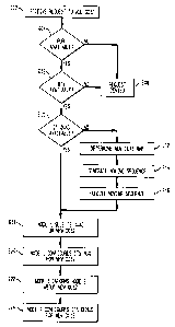
Fig. 4 shows a flow diagram of the provisioning processing implemented by
Nodes 1 and 2
of Fig. 1 to delete an existing downstream OC3 or OC 12 signal for a
particular pair of circuit
boards within Nodes 1 and 2. Node 1 receives a request from one of its local
customers to delete
an existing OC3/OC 12 signal (step 402 of Fig. 4). According to preferred
embodiments of the
present invention, provisioning processing is not permitted to delete a
customer signal if that signal
is used to recover the clock that is currently selected as the working clock
for muxing within the
node. As such, if the signal to be deleted is the current mux timing source
(step 404), then the
request is denied and the provisioning processing terminates with a failure
(step 406). Otherwise,
the signal to be deleted is not the current mux timing source and the
provisioning processing
continues to step 408.
In step 408, Node 1 configures the mux of the corresponding circuit board to
stop
combining the existing OC3/OC 12 signal into the corresponding OC48 signal. In
addition (i.e., at
the same time or just after or just before), Node 1 informs Node 2 about the
deletion of the existing
OC3/OC 12 signal (step 410) and, in response, Node 2 "deconfigures" the demux
of its
corresponding circuit board to stop handling that signal (step 412).
In preferred embodiments of the present invention, signaling between Node 1
and Node 2
(e.g., step 410 in Fig. 4) is implemented using in-band optical signaling
using selected header fields
within the OC48 frame (e.g., a dedicated data communication channel defmed in
the re-mapped
Transport Overhead (TOH) of the OC48 signal), although out-of-band optical or
electrical
signaling could be used in other embodiments. Moreover, each command
preferably relies on full
duplex handshaking involving three messages, where a transmitting node
transmits an original
CA 02353654 2001-07-24
R Antosik 2-1-2-6-1 13
command message (message #1) to a receiving node, the receiving node echoes
the received
command message (message #2) back to the transmitting node, which then
compares the echoed
command message with its original command message. If the original and echoed
command
messages match, then the transmitting node transmits an execute message
(message #3), which
authorizes the receiving node to proceed to implement the previously received
command message.
Fig. 5 shows a flow diagram of the provisioning processing implemented by
Nodes 1 and 2
of Fig. 1 to add a new downstream OC3 signal for a particular pair of circuit
boards within Nodes 1
and 2. Node 1 receives a request from one of its local customers to add the
new OC3 signal (step
502 of Fig. 5). If Node 1 determines that (1) an I/O port is not available on
the corresponding
circuit board (step 504) or (2) bandwidth is not available within the
corresponding OC48 signal
(step 506), then the request is denied and the provisioning processing
terminates with a failure
(step 508). Otherwise, Node I selects an available STS3 time slot within the
OC48 frame for the
new OC3 signal (step 510) and configures the mux of the corresponding circuit
board to start
combining the new OC3 signal into the corresponding OC48 signal (step 512). In
addition, Node I
informs Node 2 about the selected time slot for the new OC3 signal (step 514)
and, in response,
Node 2 configures the demux of its corresponding circuit board for the new OC3
signal (step 516).
In a preferred embodiment, in step 510, Node 1 searches for the most isolated,
empty STS 3
time slot to which to map the new OC3 signal. The "most isolated time slot"
refers to a time slot
where the distance (in number of used STS3 time slots) to the closest empty
STS3 time slot to the
left and to the right is maximized. The motivation for this search criterion
is to reduce the chances
of subsequently having to move that OC3 signal again in order to make room for
a new or
upgraded OC 12 signal.
Fig. 6 shows a flow diagram of the provisioning processing implemented by
Nodes I and 2
of Fig. 1 to add a new downstream OC 12 signal for a particular pair of
circuit boards within Nodes
1 and 2. Node 1 receives a request from one of its local customers to add the
new OC 12 signal
(step 602 of Fig. 6). If Node 1 determines that (1) an 1/0 port is not
available on the corresponding
circuit board (step 604) or (2) bandwidth is not available within the
corresponding OC48 signal
(step 606), then the request is denied and the provisioning processing
terminates with a failure
(step 608).
CA 02353654 2001-07-24
R Antosik 2-1-2-6-1 14
Otherwise, Node 1 determines whether a quad (i.e., a set of four consecutive
STS3 time
slots) is available in the OC48 frame for the new OC 12 signal (step 610). A
quad will be available
if all four con esponding STS3 time slots are available. If a quad is
available, then the provisioning
processing continues directly to step 618.
If, however, a quad is not available, then Mode 1 performs suitable operations
to make a
quad available. These operations will involve moving one or more existing
OC3/OC 12 signals to
different positions within the OC48 frame to change from an old OC48 map to a
new OC48 map,
where a map refers to the relationship between each OC3/OC 12 input port and
the position of the
corresponding OC3/OC 12 signal in the OC48 frame. This process of making a
quad available
involves three steps 612, 614, and 616.
During step 612, a re-map algorithm (described later in the specification in
conjunction
with Fig. 9) is executed to determine a prefened new map for the OC48 frame
with new positions
for one or more of the existing OC3/OC 12 signals within the OC48 frame that
would make a quad
available for the new OC 12 signal.
Step 614 generates a sequence of map changes (e.g., moving one or more of the
existing
OC3/OC 12 signals to new positions within the OC48 frame) that would
reconfigure the OC48
frame from the old map to the new map determined during the first phase. This
step is discussed in
further detail later in the specification after the description of Fig. 9 and
before the description of
Fig. 10.
Step 616 executes the sequence of map changes generated during step 614. This
processing is described later in the specification in conjunction with Fig.
10.
At the completion of steps 612-616, the OC48 frame will be configured in the
new map
with an empty quad available for the new OC 12 signal, and processing
continues to step 618.
At step 618, Node 1 selects the quad for the new OC 12 signal, and then
configures its mux
for the new OC 12 signal (step 620). In addition, Node I informs Node 2 about
the selected quad
for the new OC 12 signal (step 622) and, in response, Node 2 configures the
demux of its
corresponding circuit board for the new OC 12 signal (step 624).
Fig. 7 shows a flow diagram of the provisioning processing implemented by
Nodes 1 and 2
of Fig. 1 to upgrade an existing downstream OC3 signal to a new downstream OC
12 signal for a
particular pair of circuit boards within Nodes I and 2. Node 1 receives a
request from one of its
CA 02353654 2001-07-24
R Antosik 2-1-2-6-1 15
local customers to rate-upgrade an existing OC3 signal (step 702 of Fig. 7).
If Node 1 determines
that bandwidth is not available within the corresponding OC48 signal (step
704) or if the existing
OC3 signal is the current mux timing source (step 706), then the request is
denied and the
provisioning processing terminates with a failure (step 708). There will be
available bandwidth for
the rate-upgrade if there is a total of at least three available STS3 time
slots somewhere in the
OC48 frame. Note that the provisioning processing of Fig. 7 does not need to
check whether a port
is available, since it is assumed that the same port for the existing OC3
signal will be used for the
new OC 12 signal.
If there is available bandwidth for the rate-upgrade and the existing OC3
signal is not the
current mux timing source, then the existing OC3 signal is deleted (step 710),
e.g., using the
provisioning procedure of Fig. 4, and the new OC 12 signal is then added (step
712), e.g., using the
provisioning processing of Fig. 6.
Fig. 8 shows a flow diagram of the provisioning processing implemented by
Nodes 1 and 2
of Fig. 1 to downgrade an existing downstream OC 12 signal to a new downstream
OC3 signal for a
particular pair of circuit boards within Nodes 1 and 2. Node 1 receives a
request from one of its
local customers to rate-downgrade an existing OC 12 signal (step 802 of Fig.
8). If the existing
OC 12 signal is the current mux timing source (step 804), then the request is
denied and the
provisioning processing terrninates with a failure (step 806). Otherwise, the
existing OC 12 signal
is deleted (step 808), e.g., using the provisioning procedure of Fig. 4, and
the new OC3 signal is
then added (step 810), e.g., using the provisioning procedure of Fig. 5.
Figs. 4-8 show processing involved in the four different types of provisioning
for
downstream signals transmitted from Node 1 to Node 2 in Fig. 1. Those skilled
in the art will
understand that Nodes 1 and 2 are capable of implementing analogous processing
to perform the
four different types of provisioning for upstream signals transmitted from
Node 2 to Node 1. It
will be further understood that, in general, for every provisioning of a
downstream signal,
reciprocal provisioning processing will be implemented (either simultaneously
or consecutively) to
perform similar provisioning of a conesponding upstream signal.
The provisioning processing of the present invention proposes a complete error-
free
solution for automatic off-line and in-line provisioning to add/delete/rate-
upgrade/rate-downgrade
OC3/OC 12 signals in a bi-directional transmission in a TDM or DWDM network.
To make
CA 02353654 2001-07-24
R Antosik 2-1-2-6-1 16
user-provisioning in the muxing node independent of the provisioning in the
demuxing node,
according to certain embodiments of the present invention, two provisioning
commands are
preferably executed: one in the muxing node and another (an identical one) in
the demuxing node.
Execution of the two identical commands allows detection of user data entry
errors. Each
command gives the port number and bit-rate of the provisioned signal. Before
executing the
provisioning processing, the OC48 optical signals in both directions should be
active and have no
outstanding alarms.
Fig. 9 shows a flow diagram of the re-map processing of step 612 of Fig. 6
implemented to
determine a new map for the OC48 frame when a new OC 12 signal needs to be
added to an
existing (i.e., old) map, according to one embodiment of the present
invention. The processing of
Fig. 9 is based on a number of operating constraints. One of these constraints
is that, if an
OC3/OC 12 signal needs to be moved, it will be moved to a position later in
the OC48 frame (i.e.,
to higher numbered STS3 time slots). Another constraint is that, if an OC3
signal needs to be
moved, it will be moved to the most isolated, empty STS3 time slot in the OC48
frame. In some
implementations, OC3 signals may be moved only to STS3 time slots that are
later in the OC48
frame, although this constraint may be relaxed in other implementations. Yet
another constraint is
that the re-map processing selects a map that requires the minimum number of
signals to be moved
in order to minimize the impact to existing customers. The re-map processing
has the additional
constraint of not being permitted to move a signal that is used as the timing
source for muxing. In
alternative embodiments of the present invention, one or more of the operating
principles may be
relaxed or replaced by other criteria. For example, rather than minimizing the
number of signals
moved, the re-map processing may simply select the new map based on the first
available quad.
Note that the re-map processing of Fig. 9 does not move any existing signals;
it merely determines
a preferred new map for the OC48 frame that has a quad available for the new
OC 12 signal.
The re-map processing of Fig. 9 implements a time-slot-mapping algorithm to
determine
an optimum port-number-to-STS3-time-slot map for the new OC48 signal, where
"optimum"
means that a minimuln number of live (i.e., existing) signals have to be re-
mapped to different
STS3 time slot(s) in the new map. Re-mapping may be needed to free four
consecutive STS3 time
slots (i.e., a quad) in order to add a new OC 12 signal or to rate-upgrade an
existing OC3 signal to
an OC 12 signal.
CA 02353654 2001-07-24
R Antosik 2-1-2-6-1 17
The re-map processing of Fig. 9 uses a sliding window corresponding to a quad
(i.e., four
consecutive STS3 time slots). The re-map processing iteratively moves the
sliding window, one
STS3 time slot at a time, from the first quad (corresponding to the 15'
through 4'h STS3 time slots
in Fig. 3) to the thirteenth quad (corresponding to the 13'}'through 16"' STS3
time slots in Fig. 3).
At each position of the sliding window, the re-map processing determines
whether the
corresponding quad is a candidate for the quad to be used for the new OC 12
signal. If an existing
OC 12 signal is already positioned at the corresponding quad, then that quad
is rejected as a
candidate quad for the new OC 12 signal, since it would not make sense to move
an existing OC 12
signal out of a quad in order to position the new OC 12 signal at that same
quad. Similarly, if the
corresponding quad is already empty, then it will be as good a candidate for
the new OC 12 signal
as any other quad, since no existing signals will need to be moved to add the
new OC 12 signal.
This case is essentially handled by step 610 of Fig. 6.
If the current quad does not contain an entire OC 12 signal and is not empty,
then the re-
map processing determines where to move the OC3 signals that are in the
current quad and/or the
OC 12 signals that overlap with the current quad to make that quad available.
In order to move the
OC3/OC 12 signals from the current quad, it may first be necessary to move one
or more
OC3/OC 12 signals that are outside of the current quad. The re-map processing
of Fig. 9 handles
those cases.
At each iteration, the re-map processing determines whether the current quad
should be
retained as the best quad so far (i.e., based on minimizing the total number
of signals that need to
be moved to make the current quad available for the new OC 12 signal). At the
end of the 13't'
iteration (i.e., after testing all 13 quads), the re-map processing of Fig. 9
will have identified an
optimal quad to make available for the new OC 12 signal as well as a new
mapping for the existing
OC3/OC 12 signals that leaves that optimal quad empty.
In Fig. 9, the STS3 time slots are numbered from STS3_1 through STS3_16, where
STS3_1 corresponds to the first STS3 time slot relative to the current
position of the sliding
window. When the sliding window is positioned at the ls' STS3 time slot,
STS3_1 corresponds to
the ls' STS3 time slot and STS3_16 corresponds to the W' STS3 time slot. When
the sliding
window is positioned at the 2 d STS3 time slot, however, STS3_1 corresponds to
the 2 nd STS3 time
slot, STS3_15 corresponds to the 16'hSTS3 time slot, and STS3_16 has no
meaning.
CA 02353654 2001-07-24
R Antosik 2-1-2-6-1 18
In Fig. 9, "move it" indicates execution of processing to fmd the most
isolated, empty
STS3 time slot later in the OC48 frame to which to move a live OC3 signal. An
exit through "pr"
indicates a failure to meet at least one of the specified performance
requirements (e.g., moving
more than allowed number of OC3/OC 12 signals, moving signals not allowed to
be moved as
specified by the user, or attempting to move the current mux timing source).
In particular, the re-map processing of Fig. 9 starts at step 901. At step
902, the constraint
of not being able to move an OC3/OC 12 signal that is the current mux timing
source is set as the
default performance requirement (pr). If the system allows a user to add
further performance
requirements (step 903), then the user optionally adds additional performance
requirements (e.g., a
maximum number of signals that the re-map processing is allowed to move and/or
which specific
signals can or cannot be moved) (step 904).
The sliding window is then set to select the first quad (i.e., corresponding
to the 1s' through
4'hSTS3 time slots of Fig. 3) (step 905) and a jump indicator K is set to 3
(step 906). The jump
indicator K is used to determine the destination during conditional branching
that occurs towards
the end of the flow diagram (i.e., following steps 940, 952, and 961).
If STS3_1 is not empty (step 907), then the re-map processing determines
whether the
existing signal in STS3_1 is an OC3 signal (as opposed to part of an OC 12
signal) (step 908). If
so, then the re-map processing executes the "move it" processing to identify
an empty STS3 time
slot to which to move the existing OC3 signal in STS3_1 (step 909) and the re-
map processing
jumps to processing node #2 to test STS3_2. If the signal in STS3_1 is not an
OC3 signal (step
908), then it is an OC 12 signal occupying the current quad (i.e., STS3_1
through STS3 4). If the
current quad already has an OC 12 signal, it would not make sense to move that
existing OC 12
signal and the current quad is not retained as a candidate for the new OC 12
signal. In that case, the
re-map processing jumps to processing node #6 to keep the previously retained
quad (i.e., from a
previous iteration) (step 922) before moving to test for the next iteration
(step 924).
Note that, during step 908 (and all similar steps in Fig. 9 that determine
whether a
particular existing signal in a particular STS3 time slot is an OC3 signal),
the re-map processing
determines whether or not moving that existing signal violates one of the
performance requirements
(pr). If so, then, whether or not the existing signal is an OC3 signal,
processing jumps from a "pr
CA 02353654 2001-07-24
R Antosik 2-1-2-6-1 19
source" node (e.g., node 910) to "pr destination" node 923 to test the next
quad (if any) in the
OC48 frame at step 924.
The re-map processing performs processing analogous to steps 907-909 for other
STS3
time slots to (1) determine whether the STS3 time slot is empty, (2) if not,
determine whether the
existing signal is an OC3, and (3) if so, move the existing OC3 signal to
another STS3 time slot.
In particular, if the re-map processing moves an existing OC3 signal from
STS3_2 (steps
911, 912, and 913), then the re-map processing jumps to processing node #3 to
test STS3_3. If the
existing signal in STS3_2 is not an OC3 signal (steps 911 and 912), then the
first OC 12 signal has
been found and processing continues to step 929 to test STS3_6. If STS3_2 is
empty (step 911),
then processing continues to step 914 to test STS3_3.
If the re-map processing moves an existing OC3 signal from STS3_3 (steps 914,
915, and
916), then the re-map processing jumps to processing node #4 to test STS3_4.
If the existing
signal in STS3_3 is not an OC3 signal (steps 914 and 915), then the first OC
12 signal has been
found, the jump indicator K is set to 4 (step 927), and processing continues
to step 933 to test
STS3_7. If STS3_3 is empty (step 914), then processing continues to step 917
to test STS3_4.
If the re-map processing moves an existing OC3 signal from STS3_4 (steps 917,
918, and
919), then the re-map processing jumps to processing node #5 and step 920. If
the existing signal
in STS3_4 is not an OC3 signal (steps 917 and 918), then the first OC 12
signal has been found,
the jump indicator K is set to 5 (step 928), and processing continues to step
937 to test STS3_8. If
STS3_4 is empty (step 917), then processing continues to step 920.
At step 920, if the number of signals moved for the current quad is less than
the number of
signals moved for the best quad so far, then the current quad is retained as
the best quad so far
(step 921). Otherwise, the previously retained best quad is retained (step
922). In either case, if all
13 possible quads in the OC48 frame have been tested (step 924), then the re-
map processing
terminates with the retained best quad as the quad to be selected for the new
or upgraded OC 12
signal (along with a new map for the existing OC3/OC 12 signals) (step 925).
Otherwise, all 13
quads have not yet been tested (step 924), the sliding window is moved by one
STS3 time slot (step
926), and processing returns to step 906 to test the new quad.
If STS3_6 is empty (step 929) or the re-map processing moves an existing OC3
signal
from STS3_6 (steps 929, 930, and 931), then the re-map processing shifts the
first OC 12 signal
CA 02353654 2001-07-24
R Antosik 2-1-2-6-1 20
(i.e., in STS3_2 through STS3_5) up by one STS3 time slot (i.e., to STS3_3
through STS3_6)
(step 932) and then continues to step 933 to test STS3_7. If the existing
signal in STS3_6 is not
an OC3 signal (steps 929 and 930), then the second OC 12 signal has been found
and processing
continues to step 941 to test STS3_10.
If STS3_7 is empty (step 933) or the re-map processing moves an existing OC3
signal
from STS3_7 (steps 933, 934, and 935), then the re-map processing shifts the
first OC 12 signal
(i.e., in STS3_3 through STS3_6) up by one STS3 time slot (i.e., to STS3_4
through STS3_7)
(step 936) and then continues to step 937 to test STS3_8. If the existing
signal in STS3_7 is not
an OC3 signal (steps 933 and 934), then the second OC 12 signal has been found
and processing
continues to step 945 to test STS3_11.
If STS3_8 is empty (step 937) or the re-map processing moves an existing OC3
signal
from STS3_8 (steps 937, 938, and 939), then the re-map processing shifts the
first OC 12 signal
(i.e., in STS3_4 through STS3_7) up by one STS3 time slot (i.e., to STS3_5
through STS3_8)
(step 940) and then jumps to either processing node #3, #4, or #5 depending on
the value of the
jump indicator K. If the existing signal in STS3_8 is not an OC3 signal (steps
937 and 938), then
the second OC 12 signal has been found and processing continues to step 949 to
test STS3_12.
If STS3_10 is empty (step 941) or the re-map processing moves an existing OC3
signal
from STS3_10 (steps 941, 942, and 943), then the re-map processing shifts the
second OC 12
signal (i.e., in STS3_6 through STS3_9) up by one STS3 time slot (i.e., to
STS3_7 through
STS3_10), then shifts the first OC 12 signal (i.e., in STS3_2 through STS3_5)
up by one STS3
time slot (i.e., to STS3_3 through STS3_6) (step 944), and then continues to
step 945 to test
STS3_l 1. If the existing signal in STS3_10 is not an OC3 signal (steps 941
and 942), then the
third OC 12 signal has been found and processing continues to step 953 to test
STS3_14.
If STS3_11 is empty (step 945) or the re-map processing moves an existing OC3
signal
from STS3_11 (steps 945, 946, and 947), then the re-map processing shifts the
second OC 12
signal (i.e., in STS3_7 through STS3_10) up by one STS3 time slot (i.e., to
STS3_8 through
STS3_11), then shifts the first OC 12 signal (i.e., in STS3_3 through STS3_6)
up by one STS3
time slot (i.e., to STS3_4 through STS3_7) (step 948), and then continues to
step 949 to test
STS3_12. If the existing signal in STS3_11 is not an OC3 signal (steps 945 and
946), then the
third OC12 signal has been found and processing continues to step 956 to test
STS3_15.
CA 02353654 2001-07-24
R Antosik 2-1-2-6-1 21
If STS3_12 is empty (step 949) or the re-map processing moves an existing OC3
signal
from STS3_12 (steps 949, 950, and 951), then the re-map processing shifts the
second OC12
signal (i.e., in STS3_8 through STS3_11) up by one STS3 time slot (i.e., to
STS3_9 through
STS3_12), then shifts the first OC 12 signal (i.e., in STS3_4 through STS3_7)
up by one STS3
time slot (i.e., to STS3_5 through STS3_8) (step 952), and then jumps to
either processing node
#3, #4, or #5 depending on the value of the jump indicator K. If the existing
signal in STS3_12 is
not an OC3 signal (steps 949 and 950), then the third OC 12 signal has been
found and processing
continues to step 959 to test STS3_16.
If STS3_14 is empty (step 953) or the re-map processing moves an existing OC3
signal
from STS3_14 (steps 953 and 954), then the re-map processing shifts the third
OC 12 signal (i.e.,
in STS3_10 through STS3_13) up by one STS3 time slot (i.e., to STS3_11 through
STS3_14),
then shifts the second OC 12 signal (i.e., in STS3_6 through STS3_9) up by one
STS3 time slot
(i.e., to STS3_7 through STS3_10), then shifts the first OC12 signal (i.e., in
STS3_2 through
STS3_5) up by one STS3 time slot (i.e., to STS3_3 through STS3_6) (step 955),
and then
continues to step 956 to test STS3_15.
If STS3_15 is empty (step 956) or the re-map processing moves an existing OC3
signal
from STS3_15 (steps 956 and 957), then the re-map processing shifts the third
OC 12 signal (i.e.,
in STS3_1 I through STS3_14) up by one STS3 time slot (i.e., to STS3_12
through STS3_15),
then shifts the second OC 12 signal (i.e., in STS3_7 through STS3_10) up by
one STS3 time slot
(i.e., to STS3_8 through STS3_1 1), then shifts the first OC12 signal (i.e.,
in STS3_3 through
STS3_6) up by one STS3 time slot (i.e., to STS3_4 through STS3_7) (step 958),
and then
continues to step 959 to test STS3_16.
If STS3_16 is empty (step 959) or the re-map processing moves an existing OC3
signal
from STS3_16 (steps 959 and 960), then the re-map processing shifts the third
OC 12 signal (i.e.,
in STS3_12 through STS3_15) up by one STS3 time slot (i.e., to STS3_13 through
STS3_16),
then shifts the second OC12 signal (i.e., in STS3_8 through STS3_1 1) up by
one STS3 time slot
(i.e., to STS3_9 through STS3_12), then shifts the first OC12 signal (i.e., in
STS3_4 through
STS3_7) up by one STS3 time slot (i.e., to STS3_5 through STS3_8) (step 961),
and then jumps
to either processing node #3, #4, or #5 depending on the value of the jump
indicator K.
CA 02353654 2001-07-24
R Antosik 2-1-2-6-1 22
Since there are only 16 STS3 time slots, for positions of the sliding window
beyond the 1S'
STS3 time slot, the re-map processing of Fig. 9 is terminated when the end of
the OC48 frame is
reached. For example, when the sliding window is positioned at the 2"d through
5'" STS3 time
slots, STS_16 has no meaning and the re-map processing is terminated prior to
reaching steps 959-
961.
As described earlier, the re-map processing of Fig. 9 (i.e., step 612 of Fig.
6) determines an
optimal new map for the existing OC3/OC 12 signals that has a quad available
for a new OC 12
signal. Step 614 of Fig. 6 generates a sequence of map changes to change the
OC48 frame from
the old map to the new map determined during step 612. Depending on the
particular
implementation, the process of generating the sequence of map changes of step
614 may or may not
be based on the sequence of "simulated" moves generated during step 612 to
determine the new
map.
In general, the new map will differ from the old map in that one or more of
the existing
OC3/OC 12 signals will be moved to new positions in order to provide an empty
quad within the
OC48 frame. There are a number of different algorithms for generating a
sequence of map changes
that would re-map the OC48 frame from the old map to the new map. Some of
these algorithms
may be based on one or more of the following principles.
Whenever possible, in order to minimize impact to existing customers, each
move of an
existing OC3/OC 12 signal from an old position to a new position within the
OC48 frame is
implemented using a bridging and switching technique, in which transnussion of
the signal to be
moved is initiated at the new position, while maintaining transmission of the
signal at the old
position, thereby double-casting the signal at both the old and new positions
within the OC48
frame, after which transmission at the old position is then terminated. This
is done using the
multi-casting capability of the muxing node, which allows mapping of one
signal to multiple STS3
time slots, thereby sending two copies of the same signal in different STS3
time slots.
Such double-casting assumes that the old and new positions do not overlap
(i.e., that the
old and new positions do not have any STS3 time slots in common). While this
condition will
necessarily always be satisfied when moving OC3 signals, there are certain
maps where an OC 12
signal cannot be moved using bridging and switching. For example, if the
current OC48 frame
format has three OC 12 signals -- called A, B, and C -- positioned in three
quads starting at the 3rd,
CA 02353654 2001-07-24
R Antosik 2-1-2-6-1 23
7'", and 11"' STS3 time slots, respectively, then bridging and switching
cannot be performed to
move each of signals A, B, and C in order to make a quad available to add a
fourth OC 12 signal D,
because there are no two quads available for double-casting. In that case, at
least one of the
existing OC 12 signals will have to be deleted from its old position before it
can be transmitted at
its new position. For example, signal C can be deleted, signal B can then be
double-casted at the
two quads starting at the 7'hand 13'' STS3 time slots to move signal B to the
quad starting at the
13'f' STS3 time slot, signal A can then be double-casted at the two quads
starting at the 3'd and 9'h
STS3 time slots to move signal A to the quad starting at the 13"' STS3 time
slot, signal C can then
be re-added at either the quad starting at the 15' STS3 time slot or the quad
starting at the 4" STS3
time slot. In either case, the other remaining quad will then be available for
adding the new OC 12
signal D. The processing of step 614 recognizes situations where bridging and
switching cannot be
performed and generates an appropriate sequence of map changes to achieve the
desired new map
during step 616. If, for performance reasons, bridging and switching is
required for all signal
moves, this requirement can be applied during the re-map algorithm of Fig. 9
to avoid selecting a
new map that has any signal moves that cannot be implemented using bridging
and switching.
Since, by design, the re-map algorithm of Fig. 9 selects a map corresponding
to the
minimal number of signals moved, each existing OC3 signal that gets moved,
will be moved to an
STS3 time slot that was already empty in the old map. In general, therefore,
the sequence of map
moves can start with all of the OC3 signal moves, if any, and then conclude
with all of the OC 12
signal map changes, if any, where those OC 12 signal map changes may by one-
map signal moves
or, as discussed above, two-map signal deletes-and-adds, when bridging and
switching cannot be
performed.
Fig. 10 shows the processing implemented during step 616 of Fig. 6 to execute
the
sequence of map changes generated during step 614 to re-map the OC48 frame
from the old map to
the new map determined during step 612 to make a quad available for a new OC
12 signal,
according to one embodiment of the present invention. The processing of Fig.
10 is also
implemented to add a new OC3 signal at an available STS3 time slot, to add a
new OC 12 signal to
an available quad, or to delete an existing OC3/OC 12 signal. The processing
of Fig. 10
coordinates the execution of signal moves, additions, and/or deletions between
the muxing node
and the demuxing node. The processing of Fig. 10 executes a particular
sequence of map changes
CA 02353654 2001-07-24
R Antosik 2-1-2-6-1 24
corresponding to signal moves, additions, and/or deletions, one change at a
time, from the first to
the last map change in the sequence.
In Fig. 10, "to" indicates a time-out in the muxing node whenever the map
message, or the
execute map message or the acknowledge map execution message is not detected
due to the
transmission errors of the message flag (no message). When the demuxing node
detects a parity
error in the received message, it does not send the received message back to
the muxing node,
which results in a time-out by the muxing node indicated with the "to" symbol
(parity error). "te"
indicates detection of a transmission error when matching the information in
the map transmitted
by the muxing node and received from the demuxing node. "ue" indicates
detection of a user data
entry error either in the muxing node or in the demuxing node by matching the
identical
provisioning in the two nodes. This is done after confumation of error-free
transmission of the
map.
In particular, for the current map change in the sequence, the muxing node
transmits an
appropriate map message (i.e., either an add map message, a delete map
message, or a move map
message) to the demuxing node and starts a mux time-out counter (step 1002 of
Fig. 10). An add
map message identifies the port # and STS3 time slot(s) for a new OC3/OC 12
signal to be added to
the OC48 frame. A delete map message identifies the port # and STS3 time slot
for an existing
OC3/OC 12 signal to be deleted from the OC48 frame. A move map message
identifies the port #
and new STS3 time slot(s) for an existing OC3/OC 12 signal to be moved to a
new position within
the OC48 frame.
The demuxing node receives the map message from the muxing node, checks the
received
map message for parity errors, and, if there are no parity errors, echoes the
map message back to
the muxing node and starts its own demux time-out counter (step 1004). The
demuxing node also
starts its own time out counter. If the demuxing node detects a parity error,
then a transmission
error (te) is detected and the demuxing node does nothing (i.e., it does not
echo the map message
back to the muxing node), which will eventually cause the muxing node to time
out. Transmission
errors could happen first on the way from the mux to the demux and later when
sending the
message back from the demux to the mux for matching to detect even parity
errors. Odd parity
checking in the demux detects the first error, but if the two errors cancel
each other, then matching
of transmitted and received messages in the mux will not detect the fact that
the data received by
CA 02353654 2001-07-24
R Antosik 2-1-2-6-1 25
the demux is errored. To avoid that, when an odd parity error is detected in
the demux, the message
is not sent back to time-out in the muxing node, thereby forcing re-
transmission.
The muxing node receives the echoed map message from the demuxing node,
compares the
echoed map message to the original map message it sent to the demuxing node,
and, if they match,
executes Part I of the process of mapping the muxing node based on the
original map message and
transmits an execute map message to the demuxing node (step 1006). Part I of
the mux mapping
process is described later in the specification in conjunction with Fig. 11.
If the echoed map
message does not match the original map message, then a transmission error
(te) is detected. If the
mux time-out counter times out before the muxing node receives an echoed map
message, then a
time-out (to) is detected. In either case, an error counter is incremented and
processing continues to
step 1008.
If the error counter exceeds a specified threshold N (e.g., 10) (step 1008),
then an alarm
condition is signaled at the muxing node indicating that the current map
change failed (step 1010).
Note that the failure could have occurred after one or more map changes were
successfully
implemented, in which case, some OC3/OC 12 signals may have already been re-
mapped (i.e.,
moved, added, or deleted) (comment 1012) when the processing of Fig. 10
terminates in failure
(step 1014). If the error counter does not exceed the specified threshold,
then processing returns to
step 1002, where the muxing node re-transmits the previous map message to the
demuxing node to
again attempt the same map change.
If there was no time out or transmission error, then processing continues to
step 1016,
where the muxing node transmits an execute map message to the demuxing node
and restarts its
mux time-out counter.
The demuxing node receives the execute map message from the muxing node,
performs
processing to map the demuxing node based on the original map message, and
transmits a map
execution message back to the muxing node (step 1018). The demuxing node
compares the
received port number and received number of consecutive time slots STS3 (1 or
4) with the port
number and bit'rate of the provisioned signal in the demuxing node. If they do
not agree, the
demu.Ying node sends a negative acknowledge map execution message to the
muxing node to
indicate a user data entry error, and if it is the move command, the demuxing
node un-does the
double-casting. If they agree, the demuxing node executes the add/delete/move
STS3(s) map
CA 02353654 2001-07-24
R Antosik 2-1-2-6-1 26
command based on the port number, number of consecutive time slots, and STS3
number
information received in the message. Depending on the implementation, if the
demuxing node
detects a parity error in the execute map message received from the muxing
node, the demuxing
node does not transmit a map execution message back to the muxing node,
causing the muxing
node to time out and, depending on how many time-outs have occurred, re-
transmit the execute map
message. The demux mapping process is described later in the specification in
conjunction with
Fig. 12.
The muxing node receives the map execution message from the demuxing node and
implements Part 2 of the mux mapping process (step 1020). Part 2 of the mux
mapping process is
described later in the specification in conjunction with Fig. 13. If the mux
time-out counter times
out before the muxing node receives a map execution message from the demuxing
node, then a
time-out (to) is detected at the mux. In that case, an error counter is
incremented and compared to a
specified time-out threshold N (e.g., 10) (step 1022). If the error counter
exceeds the specified
time-out threshold N, then an alarm condition is signaled at the muxing node,
indicating that a map
change failed (step 1024). As with the alarm condition of step 1010, the
failure could have
occurred after one or more map changes were successfully implemented, in which
case, some
OC3/OC 12 signals may have already been remapped (i.e., moved, added, or
deleted) (comment
1012) when the processing of Fig. 10 terminates in failure (step 1014). If the
error counter does
not exceed the specified threshold, then processing returns to step 1016,
where the muxing node re-
transmits the previous execute map message to the demux to again attempt to
complete the same
map change.
If the map execution message received by the muxing node is a negative map
execution
message, indicating that a user data entry error was detected at the demuxing
node, then a user data
entry error (ue) is detected at the mux, a corresponding alarm condition is
signaled (step 1026),
before terminating processing of the sequence of map changes in failure (step
1014).
If no time-outs or user data entry errors are detected, then processing
continues to step
1028. If the last map message in the sequence of map changes has already by
processed, then
processing terminates (step 1030). Otherwise, processing returns to step 1002
to transmit the next
map message in the sequence. The sending of a new map message and its
execution in the muxing
and the demuxing nodes is repeated until the processing of Fig. 10 completes
implementation of the
CA 02353654 2001-07-24
R Antosik 2-1-2-6-1 27
new map computed using the re-map processing of Fig. 9. An inability to
distinguish between
non-detection of the transmission-errored execution map message and the
acknowledge map
execution message would make it impossible to decide if the demuxing node
executed or not the
switch of the moved OC3/OC 12 signal based on the time-out in the muxing node
alone. To avoid
failing the moved live signal, the muxing node does not perform un-doing of
the double-casting.
Instead, the failed processing generates an appropriate alann message to the
user to indicate the
situation. To minimize the possibility of non-detection of the two messages, a
strong error
detection and correction capability is designed for them.
The map messages transmitted by the mux and demux use the following common
messaging format. Each message is four bytes long, where byte 1 is a type-of-
message flag, byte 2
is a first data byte, byte 3 is a second data byte, and byte 4 is a bitwise
parity byte for bytes 1, 2,
and 3. When messages are not sent, the idle channel byte "00000000" is
inserted into the
transmission channel.
The defmed values for the type-of-message flag (byte 1) include the following
(where "x"
designates an undefmed bit that can be either 0 or 1):
o "11000xxx" - add map message
o "11101 xxx" - delete map message
o "11111 xxx" - move map message
o "11110xxx" - execute map message
o " 11011 xx 1"- positive acknowledge execution of add/delete/move map
o"11011xx0" - negative acknowledge execution of add/delete/move map
For the execute map message and the positive and negative acknowledge
execution of
add/delete/move map messages, bytes 2 and 3 are not defmed.
For the add, delete, and move map messages, the first data byte (byte 2) has
the format
"O 11 Fabcd", where F=1 means that an OC 12 signal is added/deleted/moved, F=0
means that an
OC3 signal is added/deleted/moved, and "abcd" identifies the port number for
the OC3/OC 12
signal that is added/deleted/moved.
The second data byte (byte 3) has the format "010Fefgh", where "F" has the
same
meanings as in the first data byte and "efgh" identifies the STS3 time slot
number. For the add
map message, "efgh" identifies the STS3 time slot for new OC3/OC 12 signal.
For the move map
CA 02353654 2001-07-24
R Antosik 2-1-2-6-1 28
message, "efgh" identifies the new STS3 time slot for the existing OC3/OC 12
signal to be moved.
For the delete map message, "efgh" is not really needed, since the demuxing
node will be able to
determine the STS3 time slot for the OC3/OC 12 signal to be deleted, from the
port number (i.e.,
"abcd" in byte 2).
Fig. 11 shows a flow diagram of Part I of the process of mapping the muxing
node based
on the original map message corresponding to step 1006 of Fig. 10, according
to one embodiment
of the present invention. Part 1 corresponds to the initiation of double-
casting for the bridging and
switching of an existing OC3/OC 12 signal to a new position within the OC48
frame.
In particular, the processing of Fig. I 1 starts at step 1102 (after the
muxing node receives
an echoed map message that matches its original map message) with the original
map message
identifying the port (i.e., "abcd" in byte 2 of the map message) and,
depending on the type of map
message, the STS3 time slot (i.e., "efgh" in byte 3 of the map message)
(comment 1104). If the
map message is not a move map message (step 1106), then it is an add or delete
map message, in
which case double-casting is not needed and processing of Part I terminates
(step 1118). If the
map message is a move map message, then processing continues to step 1108,
where it is
determined whether the signal to be moved is an OC3 signal or an OC 12 signal.
If the signal to be moved is an 0C3 signal (step 1108), then the specified
port is to be re-
mapped from its current ("old") STS3 time slot to the specified new STS3 time
slot (comment
1110) and double-casting is begun by mapping the port to the new STS3 time
slot while
maintaining the mapping of the port to the old STS3 time slot (step 1112),
before terminating Part
1 at step 1118.
Otherwise, the signal to be moved is an OC 12 signal (step 1108), the
specified port is to be
re-mapped to the new quad that begins at the specified STS3 time slot (comment
1114), and
double-casting is begun by mapping the port to the new quad while maintaining
the mapping of the
port to the old quad (step 1116), before terminating Part 1 at step 1118.
Fig. 12 shows a flow diagram of the process of mapping the demuxing node based
on a
received map message corresponding to step 1018 of Fig. 10, according to one
embodiment of the
present invention. The processing of Fig. 12 starts at step 1202 after the
demuxing node receives
an execute map message from the muxing node. The processing of Fig. 12 is
based on information
contained within the previously received original map message identifying the
port and, depending
CA 02353654 2001-07-24
R Antosik 2-1-2-6-1 29
on the type of map message, the STS3 time slot (comment 1204). Note that re-
transmission of the
execute map message by the muxing node should not result in multiple
executions of the same
original map message by the demuxing node (comment 1206).
If the original map message is a delete map message (step 1208), then the
demuxing node
is to delete the OC3/OC 12 output (comment 1210). If the signal to be deleted
is an OC3 signal
(step 1212), but the demuxing node has not previously received an independent
command to delete
an OC3 signal on that same port (step 1214), then a user data entry error is
detected (comment
1216) and the processing of Fig. 12 terminates without deleting the signal
(step 1244). If,
however, the signal to be deleted is an OC3 signal (step 1212) and the
demuxing node has
previously received an independent command to delete an OC3 signal on that
same port (step
1214), then the map for the specified port is deleted (step 1218) before
processing terminates at
step 1244.
Similarly, if the signal to be deleted is an OC 12 signal (step 1212), but the
demuxing node
has not previously received an independent command to delete an OC 12 signal
on that same port
(step 1220), then a user data entry error is detected (comment 1216) and the
processing of Fig. 12
terminates without deleting the signal (step 1244). If, however, the signal to
be deleted is an OC 12
signal (step 1212) and the demuxing node has previously received an
independent command to
delete an OC 12 signal on that same port (step 1220), then the map for the
specified port is deleted
(step 1222) before processing terminates at step 1244.
If the original map message is not a delete map message (step 1208), then it
is either an
add map message or a move map message (comment 1224). Note that an add map
message deletes
any existing map for the specified port (comment 1226). If the original map
message is an add
map message (step 1228), processing continues to step 1230, which determines
whether the signal
to be added is an OC3 signal or an OC 12 signal.
If the signal to be added is an OC3 signal (step 1230), but the demuxing node
has not
previously received an independent command to add an OC3 signal or rate-
downgrade an OC 12
signal to an OC3 signal on that same port (step 1232), then a user data entry
error is detected
(comment 1234) and the processing of Fig. 12 terminates without adding the
signal (step 1244). If,
however, the signal to be added is an OC3 signal (step 1230) and the demuxing
node has
previously received an independent command to add an OC3 signal or rate-
downgrade an OC 12
CA 02353654 2001-07-24
R Antosik 2-1-2-6-1 30
signal to an OC3 signal on that same port (step 1232), then the specified port
is mapped to the
specified STS3 time slot (step 1236) before processing terminates at step
1244.
Similarly, if the signal to be added is an OC 12 signal (step 1230), but the
demuxing node
has not previously received an independent command to add an OC 12 signal or
rate-upgrade an
OC3 signal to an OC 12 signal on that same port (step 1238), then a user data
entry error is
detected (comment 1234) and the processing of Fig. 12 terminates without
adding the signal (step
1244). If, however, the signal to be added is an OC 12 signal (step 1230) and
the demuxing node
has previously received an independent command to add an OC 12 signal or rate-
upgrade an 00
signal to an OC 12 signal on that same port (step 1238), then the specified
port is mapped to the
quad that starts at the specified STS3 time slot (step 1240) before processing
terminates at step
1244.
If the original map message is not an add map message (step 1228), then it is
a move map
message and processing continues to step 1242, which determines whether the
signal to be moved
is an OC3 signal or an OC 12 signal. If the signal to be moved is an OC3
signal (step 1242), then
the port is mapped to the specified new STS3 time slot (step 1236) before
processing terminates at
step 1244. If the signal to be moved is an OC 12 signal (step 1242), then the
port is mapped to the
quad that starts at the specified new STS3 time slot (step 1240) before
processing terminates at
step 1244.
Fig. 13 shows a flow diagram of Part 2 of the process of mapping the muxing
node based
on the original map message corresponding to step 1020 of Fig. 10, according
to one embodiment
of the present invention. Part 2 corresponds to the completion of the bridging
and switching of an
existing OC3/OC 12 signal to a new position within the OC48 frame.
In particular, the processing of Fig. 13 begins at step 1302 after the muxing
node receives
an acknowledge map execution message from the demuxing node. If the muxing
node received a
negative acknowledge map execution message (step 1304), then the demuxing node
detected a user
data entry error during the processing of Fig. 12 (comment 1306), in which
case, if appropnate, the
muxing node deletes the new map created during the Part 1 processing of Fig.
11 corresponding to
the initiation of double-casting (step 1308) and jumps to the "ue" node in
Fig. 10 (step 1310).
Otherwise, the muxing node received a positive acknowledge map execution
message (step
1304) and the original map message identifies the port number and, depending
on the type of map
CA 02353654 2001-07-24
R Antosik 2-1-2-6-1 31
message, the STS3 time slot (comment 1312) and processing continues to step
1314. If the map
message is a move map message (step 1314) and the signal to be moved is an 0C3
signal (step
1316), then the port is to be re-mapped to the specified new STS3 time slot
(comment 1318). Note
that, in this case, the port has already been mapped to double-cast the OC3
signal to both the old
and new STS3 time slots as a result of Part 1 of Fig. 11. As such, when the
map from the port to
the old STS3 time slot is deleted (step 1320), the map from the port to the
new STS3 time slot
remains (comment 1322) when the processing of Fig. 13 terminates (step 1342).
If, however, the signal to be moved is an OC 12 signal (step 1316), then the
port is to be re-
mapped to a new quad starting at the specified STS3 time slot (comment 1324).
Note that, in this
case, the port has already been mapped to double-cast the OC 12 signal to both
the old and new
quads as a result of Part 1 of Fig. 11. As such, when the map from the port to
the old quad is
deleted (step 1326), the map from the port to the new quad remains (comment
1328) when the
processing of Fig. 13 terminates (step 1342).
If, instead of being a move map message (step 1314), the map message is an add
map
message (step 1330), then any existing map for the specified port will be
deleted (comment 1332).
If the signal to be added is an OC3 signal (step 1334), then the specified
port is mapped to the
specified STS3 time slot (step 1336) before the processing of Fig. 13
terminates at step 1342. If,
however, the signal to be added is an OC 12 signal (step 1334), then the
specified port is mapped to
the quad that starts at the specified STS3 time slot (step 1338) before the
processing of Fig. 13
terminates at step 1342.
Otherwise, the map message is a delete map message (step 1330) and the map of
the
specified port is deleted (step 1340) before the processing of Fig. 13
terminates at step 1342.
Fig. 14 shows a block diagram of an interface circuit 1400 that performs the
provisioning
processing, according to one embodiment of the present invention. Interface
circuit 1400 is
preferably implemented on a field-programmable gate array (FPGA). After the
configuration and
initialization process, interface circuit 1400 functions as a three-port
device (i.e., with Ports A, B,
and C). Ports A and B are uni-directional interfaces to/from the SONET/SDH
mux/demux device
shown, for example, in Fig. 1. Each of Ports A and B comprise a uni-
directional 4-bit data bus,
20.736-MHZ mux and demux clocks, 8-KHz Start Of Frame (SOF) pulses, and a TOH
insert
enable pulse. Port C is a bi-directional 1/0 port that interfaces interface
circuit 1400 with the board
CA 02353654 2001-07-24
R Antosik 2-1-2-6-1 32
controller (not shown), which initiates sending of a message by writing the
message to interface
circuit 1400. When interrupted by an interface circuit that detects the
received message flag, the
board controller reads the message from that interface circuit.
Features and options of interface circuit 1400 include:
o Serial clock and high-speed data interface to the TOH of the OC-48 SONET/SDH
signal at
the output from the SONET/SDH mux and at the input to the SONET/SDH demux.
o Insertion/extraction of n-bytes of information to/from the muxed/demuxed
OC48 TOH for
the purpose of off-line and in-line user provisioning to
add/delete/rate-upgrade/rate-downgrade of mixed-rate OC-48 SONET/SDH signals.
o TOH Message Extraction (TME) Interface from the demuxed OC48 signal.
o TOH Message Insertion (TMI) Interface to the muxed OC48 signal.
o Programmable in the TME and in the TMI message width.
o Programmable in the TME and in the TMI placement of the message in the OC48
TOH.
o Add/delete/rate-upgrade/rate-downgrade message monitoring and processing.
o Parallel bi-directional asynchronous/synchronous interface to the board
controller.
o Generation of an interrupt to the board controller upon detection of a valid
message.
o Total read/write functionality from/to board controller.
o Tri-stateable outputs for In-Circuit-Test (ICT), and net sharing.
Fig. 15 shows a block diagram of muxing/demuxing circuit 1500 for the
mux/demux board
of Node 1 of Fig. 1, according to one embodiment of the present invention.
Circuit 1500 receives
up to eight OC3/OC 12-rate incoming customer signals 114 and generates a
corresponding OC48-
rate output signal for splitting, conversion, and transmission over optical
fibers 106 and 108 to
Node 2. In addition, circuit 1500 receives the two copies of the OC48-rate
signal (referred to in
Fig. 15 as OC48 input #1 and OC48 input #2) received from Node 2 over optical
fibers 110 and
112 and generates the (up to) eight corresponding OC3/OC 12-rate outgoing
customer signals 120.
In addition, circuit 1500 receives various status and control signals from a
board controller (not
shown) that controls the operations of circuit 1500. At the heart of circuit
1500 is integrated
circuitry 1502 that performs the muxing and demuxing operations.
To perform these functions, circuit 1500 generates up to 11 different clock
signals: one
clock from each of the up to eight different OC3/OC 12-rate incoming customer
signals 114, one
CA 02353654 2001-07-24
R Antosik 2-1-2-6-1 33
clock from each copy of the OC48-rate signal, and a local clock (e.g., a
Stratum-3 clock). Circuit
1500 can be configured for use in either the add/drop configuration of Fig. 1
or the drop/continue
configuration of Fig. 2. When configured for use in an add/drop configuration,
circuit 1500 selects
and uses one of the 11 different clock signals for muxing, while demuxing is
based on a clock
selected from the two OC48-rate clocks and the local clock. When configured
for use in a
drop/continue configuration, there are no incoming customer signals. As such,
both muxing and
demuxing are based on the same clock selected from the two OC48-rate clocks
and the local clock.
In particular, transceiver circuitry 1504 with appropriate clock-and-data-
recovery (CDR)
circuitry recovers the up to eight different customer signal clocks 1506 from
the up to eight
different OC3/OC 12-rate incoming customer signals 114. Customer signal clocks
generated from
OC3 signals have a clock rate of 155 MHZ, while customer signal clocks
generated from OC 12
signals have a clock rate of 622 MHZ. A control signal MSEL[1:8] from the
board controller
identifies which of the eight input ports of transceiver circuitry 1504 have
live incoming customer
signals.
The up to eight customer signal clocks 1506 are input to AND block 1508, which
applies a
logical "AND" operation between each customer signal clock 1506 and a
corresponding alarm
control signa11510 that indicates whether the corresponding clock is valid. In
particular, each of
the eight alarm control signals 1510 will have a logical value of "1" if the
corresponding customer
signal clock 1506 is valid and a logical value of "0" if a loss-of-signal
(LOS), a loss-of-clock
(LOC), an out-of-frame (OOF), or a loss-of-frame (LOF) condition exists for
that customer signal.
One of the first four customer signal clocks from AND block 1508 is selected
at mux M3 based on
control signal CSEL[3:4], while one of the last four customer signal clocks is
selected at mux M4
based on control signal CSEL[5:6].
These two selected customer signal clocks are then input to mux M5 along with
a loop-
timing clock 1512 (described below). Based on control signal CSEL[1:2], mux M5
selects one of
these three clocks. Depending on whether the incoming customer signals are OC3
or OC 12 signals
and depending on which clocks are selected by muxes M3, M4, and M5, the clock
selected by mux
M5 may have a clock rate of either 155 MHZ or 622 MHZ. When enabled by control
signal DIV4.
divider DIV4 divides the clock from mux M5 by four, and mux M6 selects either
the clock received
directly from mux M5 or the divided clock from divider DIV4 based on control
signal ENOC 12. In
CA 02353654 2001-07-24
R Antosik 2-1-2-6-1 34
particular, when the clock selected by mux M5 has a clock rate of 155 MHZ,
then mux M6 selects
the clock received directly from mux M5. When the clock selected by mux M5 has
a clock rate of
622 MHZ, then mux M6 selects the divided clock from divider DIV4. In either
case, the clock
from mux M6 has a clock rate of 155 MHZ.
The 155-MHZ clock from mux M6 is input to mux M8 along with a 155-MHZ local
clock
from local clock generator 1514. Mux M8 selects one of these two clocks based
on a control signal
1516 generated by flip-flop FFl. The clock from mux M8 is input to loss-of-
clock (LOC) detector
1518, which monitors the clock from mux M8 to detect a loss-of-clock
condition. LOC detector
1518 generates an LOC signal 1520, which is fed back to flip-flop FF 1. In
addition, LOC signal
1520 is transmitted to the board controller as GPIO(53), part of general
purpose input/output.
Control signal 1516 is also fed back to flip-flop FF 1. Whenever LOC detector
1518 detects an
LOC condition, LOC signal 1520 goes high, which causes flip-flop FF 1 to
toggle control signal
1516, thereby changing the selection made by mux M8 from one input to the
other. Control signal
1516 is also transmitted to the board controller as part of GPIO, in
particular, as GPIO(54). Flip-
flop FFI also receives preset and clear signals MXSELO and MXSEL 1,
respectively, from the
board controller.
The 155-MHZ clock selected by mux M8 is also input to mux phase-locked loop
(PLL)
1522, which multiplies the 155-MHZ clock by four to generate a 622-MHZ clock
1524, which is
input to mux/demux circuitry 1502 for use as the muxing clock for muxing the
recovered incoming
customer data signals 1526 from transceiver circuitry 1504. The resulting
muxed data signals are
presented at the mux data output of mux/demux circuitry 1502 as 16 parallel
155-Mb/s data
signals.
Meanwhile, OC48 input signal # 1 is input to CDR circuit 1528, which recovers
16 parallel
155-Mb/s data signals 1530 and a single 155-MHZ clock (CDRCLKI) 1532.
Similarly, OC48
input signal #2 is input to CDR circuit 1534, which recovers 16 parallel 155-
Mb/s data signals
1536 and a single 155-MHZ (CDRCLK2) clock 1538. The two sets of data signals
are input to
data mux 1540, which selects one of the two sets based on control signal
SEL_DATA as the data
input for demuxing by mux/demux circuitry 1502.
The two 155-MHZ clocks 1532 and 1538 are input to clock mux 1542, which
selects one
of the two clocks based on control signal SEL_DATA. Muxes 1540 and 1542 are
part of fault
CA 02353654 2001-07-24
R Antosik 2-1-2-6-1 35
protection circuitry for circuit 1500 The clock selected by mux 1542 is input
to mux 1544, which
also receives the 155-MHZ local clock from local clock generator 1514. Based
on control signals
SEL_CLK, mux 1544 selects one of the two clocks as clock 1512. In addition to
being input to
mux M5 as the loop-timing clock (as described above), clock 1512 is input to
mux/demux circuitry
1502 for use as the system clock. Clock 1512 is also input to demux PLL 1546,
which multiplies
155-MHZ clock 1512 by four to generate a 622-MHZ clock.
The 622-MHZ clock from demux PLL 1546 is input to mux M7 along with the 622-
MHZ
clock 1524 from mux PLL 1522. Based on control signal DAN_DMUX, mux M7 selects
one of
the two clocks for use by mux/demux circuitry 1502 as the demux clock for
demuxing the 16
parallel 155-Mb/s data signals from data mux 1540. When circuit 1500 is
configured for use in an
add/drop configuration, mux M7 is configured by control signal DAN_DMUX to
always select the
clock from demux PLL 1546. Alternatively, when circuit 1500 is configured for
use in a
drop/continue configuration, mux M7 is configured by control signal DAN_DMUX
to always
select clock 1524 from mux PLL 1522. In either case, the demuxed data signals
generated by
mux/demux circuitry 1502 are presented at the OC3/OC 12 data 1/0 port of
mux/demux circuitry
1502 as eight 155/622-Mb/s data signals and transmitted to transceiver
circuitry 1504 as part of
bi-directional signals 1526 for transmission to the appropriate customers as
outgoing OC3/OC 12-
rate customer signals.
The CDRCLKI and CDRCLK2 clocks 1532 and 1538 are also input to mux M1, which
selects one of the two 155-MHZ clocks based on control signal SEL_MXCLK. The
clock from
mux M 1 is input to mux M2 along with the 155-MHZ mux clock from mux/demux
circuitry 1502.
This mux clock is the same clock input to mux/demux circuitry 1502 from mux
PLL 1522. Based
on control signal SEL_TXCLK, mux M2 selects one of the two 155-MHZ clocks for
use by
transmitter 1548 in transmitting the 16 parallel 155-Mb/s data signals
generated by mux/demux
circuitry 1502 as a single OC48-rate output signal.
Circuit 1500 provides a reliable, high-performance solution for timing of
boards designed
for bi-directional muxing and demuxing of mixed-rate OC3/OC 12 signals in the
add/drop and the
drop/continue configurations of Figs. 1 and 2, respectively, in a DWDM
network.
For the bi-directional add/drop application of Fig. 1, there are two boards in
two nodes, and
a total of four muxing and demuxing time domains are timed with user- or
system-selected timing
CA 02353654 2001-07-24
R Antosik 2-1-2-6-1 36
sources to establish bi-directional transmission. As described earlier in the
context of Fig. 1, each
muxed OC48 signal from one node is split into two optical signals and carried
through physically
diverse routes. The two optical signals are received by the demux of the other
node. The demux
selects one of the inputs for demuxing.
To minimize SONET/SDH pointer adjustments in the demux, the two demux timing
domains are timed with the clock recovered from the currently selected OC48
input (as specified by
control signal SEL_DATA). The timing source for the demux domain is not
selected by the user.
A protection switch from the selected to the second OC48 input is followed by
an automatic switch
of the timing source to the clock recovered from that input. When a failure of
both OC48 inputs is
detected (as specified by control signal SEL_CLK), the demux timing source is
switched to the
local clock from generator 1514.
Muxing timing sources are selected by the user. The user gives priority for
each timing
source, highest priority (P3) for the muxing clock, second priority (P2) for
its backup, and third
priority (P 1) for the backup of the backup. All remaining timing sources are
given the lowest
priority (P0) that inhibits their use as the muxing source. Protection
switching ffrom the muxing
clock to the P2 backup clock, and from the P2 backup clock to the P 1 backup
clock is revertive.
This means that as soon as the failed clock is fixed, its status is changed to
the same as before the
failure (i.e., to be the muxing clock or the P2 backup clock). In one
implementation, the local clock
is always selected as either the muxing clock or as P2 backup clock of the
muxing clock.
A failure of the muxing clock is hardware-detected by the local loss-of-clock
(LOC)
detector 1518 and autonomously hardware-switched to the backup clock. A
protection switch to
the valid P2 backup clock is a fast hardware switch, because it is implemented
by local LOC
detector 1518. A protection switch to the valid P 1 backup clock in the
presence of the failed P2
backup clock is a slower software switch, which is implemented by the remote
board controller.
High reliability of local clock generator 1514 minimizes the probability of
the slower protection
switch.
Each clock is in one of the two states: "valid" or "invalid." The OC3/OC 12
input clocks
are invalidated upon detection of an OOF, LOF, LOC, LOS, or line-alarm-
indication-signal (LAIS)
condition. When an input clock is selected as the muxing clock, it is
invalidated and switched to
the backup clock upon detection of the "holdover" state of the S 1
synchronization byte, indicating
CA 02353654 2001-07-24
R Antosik 2-1-2-6-1 37
that the signal from which the clock is recovered, is timed with a low
accuracy clock. The OC48
input clock is invalidated upon detection of the OOF/LOF/LOC/LOS condition.
The local clock is
invalidated upon detection of the LOC condition at its output. The user
queries the state of the S 1
synchronization bytes of the incoming OC3/OC 12 signals to identify high
accuracy signals and, if
such exist, uses them as the priority timing sources. When the S 1 bytes of
more than one input
signal indicate that the signals are the timing source at the customers' drop
sites, the equal
stratum-level signals not selected for muxing lose their stratum-level
traceability. Their S 1 bytes
are changed to the "don't use" state. The S I bytes of lower stratum-level
signals not selected for
muxing are not changed; they maintain their stratum-level traceability.
In the four-time-domain system, the two demuxing clocks are recovered from the
OC48
input. Since these clocks are derived from the muxing clocks, this leaves two
independent timing
sources selected for the two muxing time domains. In the data applications,
with input clocks of
less than Stratum-3 accuracy, the local Stratum-3 clock is selected as the
muxing clock and the
OC48 input clock as its backup. In this configuration, a failed local clock is
switched to the OC48
input clock leaving only one independent timing source in the four-time-domain
system. A failure
of the second local clock and a switch to its OC48 input clock backup or a
manual switch to the
OC48 input clock creates a four-time-domain system with no independent timing
source. This is an
unstable state called "timing loop" that causes a drift of the common clock
with no independent
timing source. To protect against such loop-timing problems, whenever an OC48
input clock is
selected as the muxing clock, a message is sent to the other node to
invalidate the OC48 input clock
from being selected as the muxing clock in that node.
The uni-directional drop/continue application of Fig. 2 requires one timing
domain for the
muxing and the demuxing. This is done by selection of the muxing timing source
as the timing
source for both muxing and demuxing. All the features of the timing source are
the same as the
ones of the muxing timing source described above for the add/drop application
of Fig. 1.
In operation, the board controller identifies the priority P3 muxing clock and
its priority P2
backup and selects it with muxes M3 and M4, since one of them must be one of
the clocks
recovered by transceiver circuitry 1504 from the OC3/OC 12 inputs or the OC48
input clock
recovered by CDR circuit 1528 or CDR circuit 1534. Next, the selected clock is
normalized to a
155-MHZ rate and input to mux M8. If the local clock is selected as the muxing
clock, then the
CA 02353654 2001-07-24
R Antosik 2-1-2-6-1 38
board controller switches mux M8 to select it as the muxing clock. If not,
then the local clock
should be selected as the priority P2 backup clock, and the board controller
selects the normalized
output from mux M6 as the muxing clock. Mux PLL 1522 multiplies the output
from mux M8 to
the 622-MHZ rate required by mux/demux circuitry 1502.
LOC detector 1518 detects an LOC condition and controls an automatic, hardware
switch
to the second input of mux M8. Mux M8 can also be switched by the board
controller using a
software switch. A detected LOC condition generates an interrupt to the board
controller (i.e.,
GPIO(53)) to select a new backup clock to replace the failed clock. If the
failed clock is not the
local clock, then the board controller is able to select a new backup clock
using a software switch at
muxes M3 and M4 to allow another hardware switch at mux M8 in case of a
subsequent failure of
the muxing clock. If the failed clock is the local clock, then the board
controller is not able to
replace it with a new backup clock. In that case, if the new muxing clock
fails, the subsequent
hardware switch will not be successful and should therefore be followed with a
software switch
from the board controller. This results in a slow protection switch of the
muxing clock. A second
level of protection of the muxing clock is achieved when the user assigns
priority P 1 backup clock.
With no priority P 1 backup clock, a failure of the muxing clock or the
priority P2 backup clock
raises the "no backup" alarm.
Fig. 16 shows a state transition diagram that models the protection of the
priority 3 muxing
clock P3 with the priority 2 backup clock P2, according to one embodiment of
the present
invention. In Fig. 16, the top symbol within each node of the diagram is the
muxing clock, and the
bottom symbol is its priority 2 backup. A failed clock is indicated by the
prefix "f'. In Fig. 16,
transient states are indicated with dashed circles.
Failed OC3/OC 12 input clocks and OC48 inputs clocks do not require
maintenance. On
the other hand, a failed local clock does require maintenance. When the local
clock is backed-up,
scheduled maintenance can be performed, but, when the local clock is not
backed-up, immediate
maintenance should be performed.
At state 1602 of Fig. 16, clock P3 is the muxing clock and clock P2 is its
priority 2 backup.
If clock P2 fails (fP2), then a transition to state 1604 occurs, which results
in a "no backup" alarm
1606 that interrupts the board controller to change the state of the failed
clock of "invalid." When
the P2 clock is fixed, a transition from state 1604 back to state 1602 occurs.
CA 02353654 2001-07-24
R Antosik 2-1-2-6-1 39
When at state 1602, if clock P3 fails (fP3), the failure is hardware-detected
(i.e., by LOC
detector 1518 of Fig. 15), in which case, a hardware switch S2 (flipping fP3
with P2) is
implemented (i.e., by flip-flop FF1 and mux M8 of Fig. 15) to select backup
clock P2 as the
muxing clock, resulting in transitions from state 1602 through transient state
1608 to state 1610,
where a "no backup alarm" 1612 is generated.
When at state 1610, if clock P3 gets fixed, then that condition is software-
detected (i.e., bv
the board controller) and a software switch S2 (flipping P2 with P3) is
implemented (i.e., using
control signals MXSELO and MXSELI input to flip-flop FF1 in Fig. 15) to select
fixed clock P3 as
the muxing clock, resulting in transitions from state 1610 through transient
state 1614 back to
original state 1602. This is an example of a revertive switch that ensures
that the highest priority,
valid clock is selected for muxing, with the next highest priority, valid
clock selected as its backup.
When at state 1610, if clock P2 fails, then a hardware switch S2 (flipping fP2
with fP3) is
implemented to select failed clock fP3 as the muxing clock, resulting in
transitions from state 1610
through transient state 1616 to state 1618, where a "no clock" (board failure)
alarm 1620 is
generated.
When at state 1618, if clock P2 gets fixed, then a software switch S2
(flipping fP3 with
P2) is implemented to select fixed clock P2 as the muxing clock, resulting in
transitions from state
1618 through transient state 1622 back to state 1610, where the "no backup"
alarm 1612 is once
again generated.
When at state 1618, if clock P3 gets fixed, then a transition (not shown in
Fig. 16) occurs
from state 1618 back to state 1604, where the "no backup" alarm 1606 is once
again generated.
Fig. 16 corresponds to a situation in which no priority 1 clock has been
assigned to back up
the priority 3 and priority 2 clocks. In this case, there is no protection if
both the priority 3 and
priority 2 clocks fail.
Figs. 17 and 18 show state transition diagrams that model the protection of
the priority 3
muxing clock P3 and the priority 2 backup clock P2 with the priority 1 backup
clock P 1, according
to one embodiment of the present invention. Figs. 17 and 18 rely on the same
drawing conventions
described earlier for Fig. 16. The top portion of each of Figs. 17 and 18
gives a complete state
diagram of how the states are protected (made transient) by the not-failed
priority 1 backup clock
and all transitions to the next states corresponding to failures and fixes of
the priority 1 backup
CA 02353654 2001-07-24
R Antosik 2-1-2-6-1 40
clock P 1. The bottom portion of each of Figs. 17 and 18 gives a conditional
"fix" state diagram as
the failed clocks are fixed, assuming no failures during the fix process. If a
failure does happen,
then a'board failure" alarm is raised (not shown).
An assignment of the priority 1 backup clock P 1 activates a second level of
protection in
case of failures of either the priority 2 backup clock P2 or the muxing clock
P3 or both. According
to the hardware design of Fig. 15, the local clock is always selected as the
muxing clock or as the
priority 2 backup clock. This gives two cases: (1) when the local clock is
selected as the muxing
clock P3, and (2) when the local clock is selected as the priority 2 backup
clock P2. When the local
clock is selected as the priority 3 muxing clock, the assignment of a valid,
priority 1 backup clock
makes states 1618 (fP3, fP2) and 1604 (P3, fP2) of Fig. 16 transient, thus
eliminating
corresponding "no clock" and "no backup" alarm conditions 1620 and 1604. When
the local clock
is selected as the priority 2 backup clock, the assignment of a valid,
priority 1 backup clock makes
state 1610 (P2, fP3) transient, thus eliminating corresponding "no backup"
alarm condition 1612.
The additional protection is achieved through control by the board controller
of a software
switch S 1(i.e., implemented using muxes M3, M4, and M5 in Fig. 15). While an
execution of the
software / hardware switch S2 flips the top symbol with the one underneath,
software switch S 1
flips the top symbol with the one on the bottom, or the two lowest symbols.
When the software
switch S 1 flips a failed clock symbol in the top position with a good clock
symbol in the bottom
position, this corresponds to the slow protection switch of the failed muxing
clock. High reliability
of the local clock makes this a low probability event.
According to the hardware design of Fig. 15, each state in Fig. 17 has either
good (P3) or
failed (fP3) symbol on the top two positions, which reflects the selection of
the local clock as the
preferred muxing clock. Similarly, according to the hardware design of Fig.
15, each state in Fig.
18 has either good (P2) or failed (fP2) symbol on the top two positions that
reflects the selection of
the local clock as the priority 2 backup clock. In Figs. 17 and 18, scheduled
maintenance to fix a
failed local clock is indicated with dashed lines.
In particular, referring to Fig. 17, assuming the assignment of the priority 1
back clock P 1,
non-transient state 1618 of Fig. 16 becomes transient state 1702, which would
be software-
detected (i.e., by the board controller), in which case, a software switch S
1(flipping fP2 with P 1) is
implemented to select clock P1 as the priority 2 backup clock, followed by a
software switch S2
CA 02353654 2001-07-24
R Antosik 2-1-2-6-1 41
(flipping fP3 with P 1) to select clock P 1 as the muxing clock, resulting in
transitions from transient
state 1702 through transient state 1704 to state 1706, where the "no backup
alarm" 1708 is
generated.
When at state 1706, if clock P 1 fails, then a hardware switch S2 would be
implemented
(flipping fP1 with fP3) to select failed clock fP3 as the muxing clock,
resulting in transitions from
state 1706 through transient state 1710 to state 1712, where a "no clock"
(board failure) alarm
1714 is generated.
When at state 1712, if clock P 1 gets fixed, then a software switch S2 is
implemented
(flipping fP3 with P 1) to select fixed clock P 1 as the muxing clock,
resulting in transitions from
state 1712 through transient state 1716 to back to state 1706.
When at state 1706, if clock P2 gets fixed, a revertive software switch S 1 is
implemented
(flipping P 1 with P2) to select fixed clock P2 as the muxing clock, resulting
in transitions from
state 1706 through transient state 1718 to state 1720, where a "no backup"
alarm 1722 is
generated.
When at state 1720, if clock P3 gets fixed, a revertive software switch S2 is
implemented
(flipping P2 with P3) to select fixed clock P3 as the muxing clock, resulting
in transitions from
state 1720 through transient state 1724 to state 1726, which is equivalent to
state 1602 of Fig. 16
with an assigned priority 1 backup clock P I.
When at state 1706, if clock P3 gets fixed, a revertive software switch S2 is
implemented
(flipping P l with P3) to select fixed clock P3 as the muxing clock, resulting
in transitions from
state 1706 through transient state 1728 to state 1730.
Similarly, assuming the assignment of the priority 1 backup clock P 1, non-
transient state
1604 of Fig. 16 becomes transient state 1732, which would be software-detected
(i.e., by the board
controller), in which case, a software switch S 1(flipping fP2 with P 1) is
implemented to select
clock P 1 as the priority 2 backup clock, resulting in a transition from
transient state 1732 to state
1730.
When at state 1730, if clock P3 fails, then a hardware switch S2 would be
implemented
(flipping fP3 with P 1) to select clock P 1 as the muxing clock, resulting in
transitions from state
1730 through transient state 1734 to state 1706, where the "no backup" alarm
1708 is generated.
CA 02353654 2001-07-24
R Antosik 2-1-2-6-1 42
When at state 1730, if clock P 1 fails, then a transition from state 1730 to
state 1736
occurs, where the "no backup" alarm 1708 is generated.
When at state 1736, if clock P2 gets fixed, then a software switch S 1 would
be
implemented (flipping fP 1 with P2) to select clock P2 as the priority 2
backup clock, resulting in
transitions from state 1736 through transient state 1738 to state 1726. The
transition from
transient state 1738 to state 1726 is achieved by the board controller
replacing the failed backup
clock fP 1 with another valid backup clock P 1. As soon as the board
controller selects a new
backup clock P 1, a software switch S 1 is implemented directly to that clock,
resulting in a direct
transition to state 1726, where all clocks are valid.
When at state 1736, if clock P 1 gets fixed, then a transition from state 1736
back to state
1730 occurs (not shown in Fig. 17).
When at state 1736, if clock P3 fails, then a hardware switch S2 would be
implemented
(flipping fP3 with fP 1) to select failed clock fP 1 as the muxing clock,
resulting in a transition from
state 1736 through a transient state corresponding to (fP3, fP1, fP2) to a
state corresponding to
(fP 1, fP3, fP2) (neither shown in Fig. 17), which is substantially equivalent
to state 1712, where a
"no clock" (board failure) alarm similar to alarm 1714 is generated.
When at state 1730, if clock P2 gets fixed, a revertive software switch S 1 is
implemented
(flipping P 1 with P2) to select fixed clock P2 as the priority 2 backup
clock, resulting in transitions
from state 1730 through transient state 1740 to state 1726.
Referring to Fig. 18, assuming the assignment of the priority 1 back clock P
1, non-
transient state 1610 of Fig. 16 becomes transient state 1802, which would be
software-detected
(i.e., by the board controller), in which case, a software switch S 1(flipping
fP3 with P 1) is
implemented to select clock P 1 as the priority 2 backup clock, resulting in
transitions from transient
state 1802 to state 1804.
When at state 1804, if clock P3 gets fixed, then a revertive software switch S
1 would be
implemented (flipping P1 with P3) followed by a revertive software switch S2
(flipping P2 with
P3) to select fixed clock P3 as the muxing clock and clock P2 as the priority
2 backup clock,
resulting in transitions from state 1804 through transient states 1806 and
1808 to state 1810, which
is equivalent to state 1602 of Fig. 16.
CA 02353654 2001-07-24
R Antosik 2-1-2-6-1 43
When at state 1804, if clock P 1 fails, then a transition from state 1804 to
state 1812
occurs, where a "no backup" alarm 1814 is generated.
When at state 1812, if clock P 1 gets fixed, then a transition from state 1812
back to state
1804 occurs.
When at state 1812, if clock P3 gets fixed, then a software switch S 1 would
be
implemented (flipping fP1 with P3) followed by a revertive software switch S2
(flipping P2 with
P3) to select fixed clock P3 as the muxing clock and clock P2 as the priority
2 backup clock,
resulting in transitions from state 1812 through transient states 1816 and
1818 to state 1820.
When at state 1820, if clock P 1 gets fixed, then a transition from state 1820
to state 1810
occurs.
When at state 1804, if clock P2 fails, then a software switch is implemented
(flipping fP2
with P 1) to select clock P 1 as the muxing clock, resulting in transitions
from state 1804 through
transient state 1822 to state 1824, where a "no backup" alarm 1826 is
generated.
When at state 1824, if clock P 1 fails, then a hardware switch S2 is
implemented (flipping
fP 1 with fP2) to select failed clock fP2 as the muxing clock, resulting in
transitions from state 1824
through transient state 1828 to state 1830, where a "no clock" (board failure)
alarm occurs 1832.
When at state 1830, if clock P 1 gets fixed, then a software switch S2 is
implemented
(flipping fP2 with P 1) to select fixed clock P 1 as the muxing clock,
resulting in transitions from
state 1830 through transient state 1822 back to state 1824.
When at state 1824, if clock P2 gets fixed, then a revertive software switch
S2 is
implemented (flipping P 1 with P2) to select fixed clock P2 as the muxing
clock, resulting in
transitions from state 1824 through transient state 1834 to state 1836.
When at state 1836, if clock P3 gets fixed, then a revertive software switch S
1 is
implemented (flipping P 1 with P3) followed by a revertive software switch S2
(flipping P2 with
P3) to select fixed clock P3 as the muxing clock and clock P2 as the priority
2 backup clock,
resulting in transitions from state 1836 through transient states 1838 and
1840 to state 1810.
When at state 1824, if clock P3 gets fixed, then a revertive software switch
S2 is
implemented (flipping P1 with P3) to select fixed clock P3 as the muxing
clock, resulting in
transitions from state 1824 through transient state 1842 to state 1844, where
the "no backup"
alarm 1826 is generated.
CA 02353654 2001-07-24
R Antosik 2-1-2-6-1 44
When at state 1844, if clock P2 gets fixed, then a transition from state 1844
to state 1810
occurs.
As before, the assignment of the priority 1 back clock P 1 causes non-
transient state 1618
of Fig. 16 to become transient state 1846, which would be software-detected
(i.e., by the board
controller), in which case, a software switch S 1(flipping fP3 with P 1) is
implemented to select
clock P 1 as the muxing clock, resulting in transitions from transient state
1846 to state 1824.
The present invention has been described in the context of an OC48 frame in
which each
OC 12 signal must be positioned within a quad (i.e., four consecutive STS3
time slots). It
alternative implementations of the present invention, this criterion may be
relaxed. For example, in
some implementations, circular symmetry may be allowed, in which an OC 12
signal may "wrap
around" within the OC48 frame. For example, an OC 12 signal may be positioned
at the 14'}', 15'h
16'", and ls' STS3 time slots, starting at the 14'1 STS3 time slot and ending
at the ls' STS3 time
slot. Moreover, in some implementations, an OC 12 signal may be positioned
within any four STS3
time slots, whether they are consecutive or not.
Although the present invention has been described in the context of circuit
boards that can
handle up to eight different OC3/OC 12 customer signals in each direction,
those skilled in the art
will understand that, in alternative embodiments, up to 16 different 0C3-rate
signals could be
packed into a single OC48 optical signal.
Although the present invention has been described in the context of nodes for
SONET-
based DWDM optical communication networks that support OC3, OC 12, and OC48
signals, those
skilled in the art will understand that alternative embodiments of the present
invention could be
implemented for other signal rates (e.g., combining OC3, OC 12, and OC48
signals into OC 192
signals), for multiplexing other than DWDM including time division
multiplexing (TDM), and/or
for communication protocols other than SONET.
It will be further understood that various changes in the details, materials,
and
arrangements of the parts which have been described and illustrated in order
to explain the nature
of this invention may be made by those skilled in the art without departing
from the scope of the
invention as expressed in the following claims.