Note: Descriptions are shown in the official language in which they were submitted.
CA 02353927 2001-06-06
WO 00!35048 PCT/US99/29095
BALANCED DIPOLE ANTENNA FOR MOBILE PHONES
BACKGROUND OF THE INVENTION
I. Field of the Invention
The present invention relates generally to antennas. More specifically,
the present invention relates to a balanced dipole antenna for mobile phones.
II. Description of the Related Art
Recent advancements in electronics have significantly improved the
performance of mobile phones. For example, advancements in integrated
circuit technology have led to high performance radio frequency (RF) circuits.
The RF circuits are used to construct transmitters, receivers and other signal
processing components typically found in mobille phones. Also, advancements
in integrated circuit technology have led to a reduction in the size of RF
circuits,
thereby leading to a reduction in the overall size of a mobile phone.
Similarly, advancements in battery technology have resulted in smaller,
lighter and longer lasting batteries used in mobile phones. These advancements
have resulted in smaller and lighter mobile phones that operate for a longer
period of time on a single charge.
Generally, a user of a mobile phone must be able to communicate with
another user or a ground station that can be located in any direction from the
user. For this reason, the antenna in the user's mobile phone must be able to
receive and transmit signals from and in all directions. Consequently, it is
desirable that the antenna exhibit a symmetric radiation pattern having a
uniform gain in the azimuth.
Unfortunately, antennas found in today's typical mobile phones do not
exhibit a symmetric radiation pattern. Mobile phones generally utilize
monopole antennas (for example, a whip antenna) that, due to the presence of
unbalanced currents, exhibit asymmetric radiation patterns. This is primarily
due to the fact that the shape and dimension o:E a monopole are not equivalent
to the shape and dimension of a ground plane of a printed wire board (PWB)
CA 02353927 2001-06-06
WO 00/35048 PCTIUS99129095
2
used as a counterpoise, resulting in an unequal current distribution in the
monopole and in the ground plane.
As a result, it has been recognized that there is a need for an antenna fox
a mobile phone that exhibits a symmetric radiation pattern.
SUMMARY OF THE INVENTION
The present invention is directed to a balanced dipole antenna for mobile
phones, such as cellular and PCS phones. The balanced dipole antenna
comprises a radiator element and _a counterpoise formed of a conducting
material. The counterpoise is electrically isolated from a printed wire board
(PWB) of the mobile phone.
A balun couples the balanced dipole antenna to a signal source. The
balun has a single input terminal and two output terminals. The input terminal
is connected to the signal source. The first and second output terminals are
connected to the radiator element and the counterpoise, respectively. The
balun
receives a single ended unbalanced signal from the signal source and provides
the radiator element and the counterpoise 'with first and second signals,
respectively. The first and second signals haves equal magnitude but are out
of
phase by 180 degrees. The first and second si~mals produce balanced currents
that are circulated in the radiator element and the counterpoise, thereby
producing a symmetric radiation pattern.
Further features and advantages of the invention, as well as the structure
and operation of various embodiments of the invention, are described in detail
below with reference to the accompanying dra'vings.
BRIEF DESCRIPTION OF T:HE DRAWINGS
In the drawings, like reference numb<~rs generally indicate identical,
funetianally similar, and/or structurally similar elements. The drawing in
which an element first appears is indicated by the leftmast digits) in the
reference number.
The present invention will be described with reference to the
accompanying drawings, wherein:
FIG. 1 illustrates a monopole antenna used in a typical mobile phone;
FIG. 2 shows current vectors in a monopole antenna;
CA 02353927 2001-06-06
PCT/i.1S99/29095
WO 00J3S048
FIG. 3 illustrates a dipole antenna;
FIG. 4 shows current distributions in dipole antennas of different
lengths;
FIG. 5A illustrates the radiation patterns of a half wavelength dipole
antenna;
FIG. 5B illustrates the radiation patteo-n of a full wavelength dipole
antenna;
FIG. 6 illustrates a balanced dipole antenna according to one
embodiment of the present invention;
FIGS. 7A and 7B illustrate ~computex~ simulated field patterns of a
conventional antenna;
FIGS. SA and 8B illustrate computer simulated field patterns of a
balanced dipole antenna according to one embodiment; and
FIGS. 9, 10 and 11 ~ illustrate baluns in accordance with three
embodiments of the present invention.
DETAILED DESCRIPTION OF THE PREFERRED
EMBODIMEI'STS
I. Overview of the Present Invention
As noted before, antennas found in today's typical mobile phones do not
exhibit a symmetric radiation pattern. rVlobile phones generally utilize
monopole antennas that, due to the presence of unbalanced currents, exhibit
asymmetric radiation patterns. This is illustrated further in FIGS.1 and 2.
FIG. 1 illustrates a monopole antenna 100 used in a typical mobile phone
101. The phone 101 contains transmit/receive circuits and other ancillary
electronic and mechanical components needed to send and receive calls and to
perform all other normal phone operations. These components are well known
and are not shown or described further as. they form no part of the present
invention. Monopole antenna 100 comprises a radiator (a monopole) 104, a
printed wire board (PWB) 108, a reactive matching network 112 and a signal
source 116. Reactive matching network 112 comprises first and second outputs
120 and 124. First output 120 is connected t:o monopole 104 and second output
CA 02353927 2001-06-06
WO 00/35048 PCT/US99/29095
4
124 is connected to ground plane 128 of PWB 108. around plane 128 acts as a
counterpoise in order to provide a return path for currents in antenna 100.
Reactive matching network 112 forms an unbalanced feed to monopole
104. The unbalanced feed causes unbalanced currents to flow along ground
plane 128. This is primarily due to the fact that the shape and dimension of
monopole 104 are not equivalent to the shape and dimension of ground plane
128, resulting in unequal current distribution in manopole 104 and in ground
plane 128. As a result, monopole 104 and ground plane 12$ form an
asymmetric dipole, thereby causing an asymmetric radiation pattern (that is, a
distorted radiation pattern}.
FIG. 2 shows the current vectors h and IZ in monopole 204 and ground
plane 128, respectively. The horizontal component IZx of the current I, in
ground plane 128 is balanced by the horizontal component Iix of the current Ir
in
monopole 104. However, the vertical component IzY of the current IZ in ground
plane 128 remains unbalanced, because of a lack of an opposing vertical
component in monopole 104. The shape and dimension of monopole 104
prevent the formation of a vertical component of t:he current vector Ir. As a
result, unbalanced currents flow along ground plane 128, causing a distorted
radiation pattern.
Furthermore, monopole antenna 100 provides less flexibility as its
radiation pattern is driven by the size and /or shape of PWB 108. Since the
size
and/or shape of PWB 108 are driven in large part by the size and/or shape of
the mobile phone's case that houses PWB 108, designers are often handicapped
in their selection of a radiation pattern by the pre-existing size and/or
shape of
a mobile phone's case.
The present invention provides a solution to the aforementioned
problems. The present invention is a balanced dipole antenna for a mobile
phone, for example, a PCS phone or a cellular phone. The present invention
advantageously incorporates a balanced dipole ante~:m.a in a mobile phone that
significantly improves the radiation pattern of a mobile phone. Furthermore,
the present invention allows designers to select desired radiation patterns
for
mobile phones without being constrained by the shape of PWBs.
Briefly stated, the balanced dipole antenna comprises a radiator element
and a counterpoise, both formed of a conducting material. The counterpoise is
CA 02353927 2001-06-06
WO 00/35048 PCT/US99/29095
electrically isolated from the ground plane of a printed wire board (PWB) of
the
mobile phone. A matching network, for example, a balun, provides balanced
current to the dipole antenna, resulting in a symmetric radiation pattern. The
balanced dipole antenna allows superior performance over conventional
5 antennas found in mobile phones today by enabling a user of a mobile phone
to
communicate uniformly in all directions, that is, 360 degrees.
As noted above, the present invention incor~>orates the advantages of a
dipole antenna in a mobile phone. Simply stated, a dipole antenna is a
diverging two-wire transmission line. FIG. 3 illustrates a dipole antenna 300.
Dipole antenna 300 comprises first and second radiators 304 and 308,
respectively, connected to a signal source 312 by a two-wire transmission line
316.
Dipole antenna 300 can be of any length L, such as L = 7~, a.J2, ?.l4, where
~,
corresponds to the wavelength of the operating frecruency f of dipole antenna
300. The current distributions in first and second radiators 304 and 30$ are
sinusoidal provided that the diameter of each radiator is less than 7~/i00.
Examples of the approximate current distributions in a number of dipole
antennas of different lengths are illustrated in FIG. 4.
Dipole antenna 300 exhibits a symmetric radiation pattern. A symmetric
radiation pattern provides uniform gain in 360 degrees, thereby allowing
equally effective communication in all directions. hIGS. 5A and 5B illustrate
the radiation pattern of dipole antenna 300 having selected lengths. The
current
distribution in dipole antenna 300 is assumed to be sinusoidal.
FIG. 5A illustrates the radiation pattern of .a dipole antenna having a
length L=71,12. The radiation pattern for L=~,/2 is given by the following
equation.
E=cos[(~/2) cos 8]I sin 8
FIG. 5B illustrates the radiation pattern of a dipole antenna having a
length L=~,. The radiation pattern for L=~, is given by the following
equation.
E=cos( ~ cos 8)+I/sin 8
CA 02353927 2001-06-06
WO 00/35048 PCTIUS99/29095
6
II. The Invention
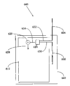
FIG. 6 illustrates a balanced dipole antenna 600 according to one
embodiment of the present invention. Antenna 600 comprises a radiator 604, a
counterpoise 608, a PWB 612 and a balun 616.
A signal source 620 is connected to balun 616. Signal source 620 has First
and second terminals 624 and 628, respectively. First terminal 624 is
connected
to balun 616, whereas second terminal 628 is grounded. In one embodiment,
signal souxce 620 is mounted on PWB 612. In o~>eration, signal source 620
provides a single ended RF signal to .balun 616 by First terminal b24.
In addition to signal source 620, PWB 612 supports on board circuitry,
such as, a receiver, a transmitter, and other signal processing circuitry
needed
fox a mobile phone's operation. PWB 612 has a grouund plane 644 that provides
a ground For ail on board circuitry.
In general, the purpose of a balun is to connect a balanced antenna to an
unbalanced source (or an unbalanced transmission line). In this embodiment,
balun 616 connects radiator 604 and counterpoise 608 to an unbalanced source,
that is, signal source 620. Since the output of signal source 620 is single
ended,
it is unbalanced. If the single ended output from signal source 620 is
directly
coupled to radiator 604 and counterpoise 608, it would result in unbalanced
currents in antenna 600. Thus, balun 616 is used to convert an unbalanced
source to a balanced source.
Balun 616 has first and second output terminals 632 and 636,
respectively. First and second output terminals 632 and 636 are connected to
radiator 604 and counterpoise 608, respectively. Balun 616 converts the single
ended signal to first and second signals that are provided to radiator 604 and
counterpoise 608, respectively. First and second signals have equal
magnitudes,
but are out of phase by 180 degrees. The operation of balun 616 is described
in
detail later.
In order for antenna 600 to operate satisfactorily, counterpoise 608 must
be electrically isolated from ground plane 644 of PWB 612. Isolation of
counterpoise 608 ensures that current will not flo~cw from counterpoise 608 to
ground plane 644. If counterpoise 608 is not electrically isolated from ground
plane 644, unbalanced currents will Flow along ground plane 644, thereby
resulting in a distorted radiation pattern. Isolation for counterpoise 608 can
be
CA 02353927 2001-06-06
WO 00/35048 PCT/US99/29095
7
provided by maintaining a gap between PWB 612 and counterpoise 608. For
example, counterpoise 608 can be placed parallel to PWB 612 as shown in FIG.
6. Alternatively, counterpoise 608 can be constructed on PWB 612 by various
known techniques described later. In that case, counterpoise 608 is generally
separated from ground plane 644 by a dielectric material.
When radiator 604 and counterpoise 608 are excited by a first and a
second signal, respectively, having equal magnitude, but which are out of
phase
by 180 degrees, balanced currents circulate in the radiator and the
counterpoise.
As a result, antenna 600 produces a symmetric radiation pattern.
Counterpoise 608 will generally be enclosed inside the mobile phone's
housing 640. In other words, counterpoise 608 will not be visible from the
outside. Radiator 604, on the other hand, will generally extend out of mobile
phone's housing 640. Thus, from the exterior, the present invention will not
alter a mobile phone's appearance.
In one embodiment, radiator 604 and counterpoise 608 have substantially
similar dimensions and/or shapes. However, radiator 604 and counterpoise
608 may have dissimilar shapes and/or dimensions. Counterpoise 608 may be
printed on PWB 612. Alternatively, counterpoise 608 may be a metallic strip
embedded in a mobile phone's case. Counterpoise 608 may be constructed
using other techniques known in the art.
Although, the balanced dipole antenna according to the present
invention has been described as a linear dipole antenna, it will become
apparent
to one skilled in the art, that the underlying concept behind the present
invention can be adapted to other antennas in mobile phones as well. In fact,
the concept of the present invention can be advantageously utilized in other
types of antennas in mobile phones to thereby provide balanced currents.
In one embodiment, the length of antenna 600 is 7~, where ~, is a
wavelength corresponding to an operating frequency. The length of the
antenna is the total length of radiator 604 and counterpoise 608. Other
lengths
can be used, such as; ~,/2, ~,/4, etc. In one embodiment, antenna 600 is sized
to
operate over a cellular frequency band (approximately 900 MHz). In another
embodiment, antenna 600 is sized to operate over a PCS frequency band
(approximately 1.9 GHz}.
CA 02353927 2001-06-06
WO 00135048 PCT/U599/29095
FIGS. 7A and 7B illustrate computer simulated field patterns of antenna
100, that is, a conventional whip antenna used in a typical mobile phone,
operating at 1.99 GHz. FIG. 7A illustrates a front f.-ace pattern 702
{measured
from the front of the mobile phone) and FIG. 7S illustrates a side view
pattern
704 {measured from the side of the mobile phone). In both cases, the field
patterns of antenna 100 are asymmetric. As a result, antenna 100 does not
transmit or receive signals uniformly in all directions.
FIGS. 8A and 8B illustrate computer simulated electric field patterns of
balanced dipole antenna 600 operating at 1.99 GHz. FIG. 8A illustrates a front
face pattern and FIG. 8B illustrates a side view pattE?rn. In both cases, the
field
patterns are quite symmetric. In the case of the front face pattern, the
maximum electric field is 2.08 dB at -5.38 degrees, while in the case of the
side
view pattern, the maximum electric field is 1.94 dB at 0 degree. FIGS. 8A and
8B clearly demonstrate the improvements in field patterns exhibited by the
balanced dipole antenna according to the present invention over a conventional
antenna.
FIG. 9 illustrates a balun 900 in accordance with one embodiment. Balun
900 receives a single ended, unbalanced signal from ;a signal source and
outputs
a balanced signal to a dipole antenna. Balun 900 comprises two inductors 904,
908 and two capacitors 912, 116. Inductor 904 and capacitor 912 are connected
at one end to a signal source 920. Inductor 908 ins connected at one end to
capacitor 912 while the other end of inductor 908 is grounded. Capacitor 916
is
connected at one end to inductor 904 while the other end of capacitor 916 is
grounded. Output signals 924 and 928 are balanced and are phase shifted from
each other by 180 degrees.
FIG. 10 illustrates a balun 1000 in accordance with another embodiment.
Balun 1000 comprises a power splitter 1004 that receives a single ended output
from a signal source 1024 and outputs a balanced signal at output terminals
1008 and 1012. An inductor or choke 1016 is connected in series to an output
terminal 1012. Output terminal 1008 is connected to a radiator 1030, while
output 1012 is connected to a counterpoise 1020 through inductor 1016.
The function of the power splitter 1004 is to split a signal from signal
source 1024 into two signals each having an equal magnitude. The first signal
is
provided to radiator 1030. The second signal is phase shifted 180° by
inductor
CA 02353927 2001-06-06
WO 00/35048 PCT/US99/29095
9
1016 and the phase shifted signal is then provided to counterpoise 1020.
Baluns
900 and 1000 are described as illustrative examples only.
PIG. 11 illustrates a folded balun 1100 that allows direct connection of a
coaxial line 1102 to a dipole antenna 1108. A coax outer conductor 1112 is
connected to a pole 1116 fed from a center conductor 1120. Coax 1112 runs
alongside a feeder coax 1104 for a quarter wavelength. Another pole 1128
connects directly to the shield of feeder coax 1104. While a few selected
baluns
have been described, it will become apparent to persons skilled in the art
that
other types of baluns can be easily used in the present invention.
While various embodiments of the present invention have been
described above, it should be understood that they have been presented by way
of example only, and not limitation. Thus, the breadth and scope of the
present
invention should not be limited by any of the above-described exemplary
embodiments, but should be defined only in accordance with the following
claims and their equivalents.
WHAT IS CLAIMED IS: