Note: Descriptions are shown in the official language in which they were submitted.
CA 02354066 2001-06-O1
WO 00/33459 PCT/US99IZ~853
DESCRIPT10N
Constant Gain Constant Phase RF Power Block
Background Of The Invention
1. Field of the Invention
S The present invention pertains generally to the field of power transistors
and, more
particularly, to methods and apparatus for providing a constant gain, constant
phase RF
power transistor block for use in, e.g., a base station receivers in a high
frequency wireless
communication networks.
2. Backeround
The use of radio frequency (RF) power transistors, for example, as amplifiers
in
wireless communication networks, is well known. With the considerable recent
growth in
the demand for wireless services, such as personal communication services
(PCS), the
operating frequency of wireless networks has increased dramatically and is now
well into
the gigahertz (GHz). At such high frequencies, consistent performance
characteristics of
RF power transistor amplifier devices becomes increasingly more complex.
In particular, RF amplifier requirements demand highly Linear performance to
meet
the demands of new digital systems, such as CDMA, HDTV, WCDMA, GSM, etc.
Cellular systems are especially demanding, because the power transistor
devices are
expected to maintain the same output characteristics, even if the main power
fails and
back-up DC battery kicks in. This is problematic, since the voltage supplied
by such back-
up DC battery systems can vary widely.
Production of IZF power transistors on a large scale basis is also a problem,
because of natural variables which the devices possess. In particular, the
transistor devices
have natural variances in output gain and signal phase shift, especially over
varying input
voltages. Thus, in commercial implementations, significant time and effort is
needed to
first characterize each RF transistor device over the range of expected
operating voltages,
and then attempt to "hme" the device to deliver a desired output gain and
phase.
However, the ability to successfully tune transistor devices is limited, due
to the fact that
the transistors will often exhibit differing gain and/or phase variations over
identical
operating voltage changes.
One known technique is to match the transistor output to a higher impedance,
c.g.,
50 ohms, which greatly reduces the possibility of variations in gain or phase
causod by
being placed in differing amplif cr circuit configurations. While this
technique can
SUBSTITUTE SHEET (RULE 26)
CA 02354066 2001-06-O1
WO 00/33459 PCT/US99~17853
2
greatly reduce problems in proving constant performance gain and phase delay
output
across different transistor devices, it does not completely solve the problem.
This is
because all RF transistors, if taken in a large enough sample size, will have
gain and phase
delay variations for any specific voltage. This variation can make large scale
production
of advanced RF amplifiers extremely time consuming and costly. Further, if the
operating
voltage provided to the amplifier changes, such as when a base station loses
main power
and goes on battery back-up, the gain and phase delay changes in the devices
will not be
known, without time consuming and expensive individual "try and fail" tuning.
By way of illustration, even if two RF transistor devices could be "tuned" in
respective identical amplifier circuits to have output gain of 11 dB gain, 6
degrees phase
change at an input voltage of 28 v dc, a drop in the input voltage to 27.5 v
do would likely
cause different results in the respective RF transistors, e.g., with the
output of one
changing to 10.9 dB and 6 degrees phase delay, and the other changing to 10.7
dB and 5.8
degrees phase delay. This difference in operating characteristics between
transistor
devices is problematic for the manufactures and users of the RF transistors.
Thus, it would be advantageous to provide RF power transistor amplifier
devices
that have a constant gain and phase delay output over a wide variation in
input voltages.
Summary Of The Invention
In accordance with a first aspect, the present invention provides a constant
gain,
constant phase RF power block, e.g., for use in a RF amplifier apparatus. In a
preferred
embodiment, the power block includes a DC to DC power supply circuit having as
an
input a varying DC voltage and as outputs a constant supply voltage and a
constant bias
voltage. A power transistor circuit is provided adjacent the power supply
circuit, the
power transistor circuit having as inputs the constant supply voltage and the
constant bias
voltage, and further configured to receive and amplify an RF signal.
In accordance with a further aspect of the invention, the power supply circuit
includes means for setting the supply and bias voltage levels. In one
preferred
embodiment, a first laser trimmable resistor is provided for setting the
supply voltage
second laser trimmable resistor is provided for setting the bias voltage. In
this manner, the
constant supply and bias voltages may be easily tuned to a desired level
during assembly
of the power block device. In. an alternate preferred embodiment, the supply
and bias
voltages are set with respective potentiometers.
In accordance with a still further aspect of the present invention, the power
supply
circuit may comprise either a sepic converter (i.e., which either steps up or
steps down the
input voltage) or a forward converter (i.e., which steps down the input
voltage).
CA 02354066 2001-06-O1
WO.00/33459 PCT/US99l17853
3
In accordance with yet another aspect of the present invention, the input and
amplified RF signals are each matched to a relatively high impedance, e.g.,
approximately
fifty ohms in a preferred embodiment.
In another preferred embodiment, the present invention provides and amplifier
apparatus, comprising a heat sink. A DC to DC power supply circuit haring as
an input a
varying DC voltage and as outputs a constant supply voltage and a constant
bias voltage,
includes a transformer housing secured to the heat sink. A power transistor
device having
as inputs the constant supply voltage and the constant bias voltage, includes
a mounting
flange secured to the heat sink. In accordance with a still further aspect of
the present
invention, the transformer housing and flange are attached to the heat sink
proximate each
other.
As will be apparent to those skilled in the art, other and further aspects and
advantages of the present invention will appear hereinafter.
Brief Description Of The Drawings
i 5 Preferred embodiments of the present invention are illustrated by way of
example,
and not by way of limitation, in the figures of the accompanying drawings, in
which like
reference numerals refer to like components, and in which:
FIG. 1 is a simplified block diagram of a constant gain, constant phase RF
power
block provided in accordance with the present invention;
FIG. 2 is a partial side view of a prototype design of preferred a constant
gain,
constant phase delay RF power block, illustrating use of a common heat sink
for the
respective dc/dc converter and RF transistor components of the power block;
FIG. 3 is a schematic illustration of a preferred dc/dc converter circuit for
use in
the RF power block of FIG. 2; and
FIG. 4 is a schematic illustration of a preferred RF amplifier circuit for use
in the
RF power block of FIG. 2.
Detailed Description Of The Preferred Embodiments
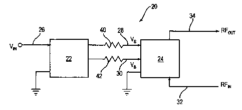
Referring to FIG. 1, a preferred constant gain, constant phase delay RF power
block 20 includes generally a DC to DC power supply circuit 22 having as an
input a
varying DC voltage 26 and as outputs a constant supply voltage 28 and a
constant bias
voltage 30. The power supply circuit 22 may be a step up; step down, or a
sepic converter,
i.e., which is capable of either stepping up or stepping dawn the input
voltage 26 to
generate the output supply voltage 28.
CA 02354066 2001-06-O1
WO 00/33459 PCTNS99/27853
4
By way of example, in one preferred embodiment, the power supply circuit 22
includes a sepic converter that can provide a constant output voltage of
approximately
twenty-eight volts DC from an input voltage 26 that may vary over a range of
nine to
thirty-six volts DC. By way of further example, in another preferred
embodiment, the
power supply circuit 22 includes a step down converter that can provide a
constant output
supply voltage of approximately twenty-eight volts DC from an input voltage 26
that may
vary over a range of thirty-six to seventy-two volts DC. As is apparent to
those skilled in
the art, any number of converter topologies may be employed, including
multiple
converter topologies, depending on the particular input voltage range that
will be
encountered in a given application and the required output supply voltage 28.
The 1tF power block 20 also generally includes an RF power transistor circuit
24,
which has as inputs the constant supply voltage 28 and the constant bias
voltage 30,
respectfully. The power transistor circuit 24 is configured to receive as a
further input an
ItF signal input 32, wherein the RF signal 32 is amplified and output 34 by
the power
transistor circuit 24.
In order to better stabilize the transistor circuit 24, which generally
operates a
relatively low impedance, both the RF input signal 32 and (amplified) output
signal are
matched to a relatively high impedance, e.g., 50 ohms in a preferred
embodiment.
A first laser trimmable resistor 40 is used to set the supply voltage, and a
second
laser trimmable resistor 42 is used to set the bias voltage. In this manner,
during
assembly, the supply and bias voltage outputs 28 and 30 may be adjusted (or
"tuned' by
laser ablation of a portion of the respective resistors 40 and 42. In an
alternate preferred
embodiment (not shown), the supply and bias voltages may be set with
respective
potentiometers.
An advantage of the RF power block 20 over the prior art is that the gain and
phase
delay of the RF output signal 34 may be held constant over a broad range of
input voltages
26. Prior to deployment of the RF power block 20 in an amplifier apparatus,
the
respective supply and bias voltages 28 and 30 are preferably tuned (i.e., by
ablating
portions of the respective resistors 40 and 42) to give the amplified RF
signal 34 a desired
gain and phase delay. Because (as explained above) each RF power transistor
will have
slightly different performance characteristics, the respective input voltages
28 and 30 may
also vary to achieve identical gain and phase delay outputs between devices.
In other
words, variations in a given RF power transistor are compensated for by
adjusting the
voltage it "sees."
By way of example, two exemplary RF power blocks (designated as 20 and 20')
may have the following characteristics: For block 20, in order to achieve a
constant output
CA 02354066 2001-06-O1
WO 00/33459 PCT/US99/Z7853
S
gain of I 1 dB and 6.2 degrees phase delay, the input supply and bias voltages
are tuned to
28.2 v and 3.S v; respectively. For block 20', in order to achieve an
identical constant
output gain of 11 dB and 6.2 degrees phase delay, the input supply and bias
voltages are
tuned to 27.9 v and 3.3 v, respectively. An advantage of this aspect of the
present
S invention, however, is that once the initially input voltages (28 and 30)
are tuned, the
output gain and phase will be substantially identical across different devices
and over a
broad range of input voltages.
Referring to FIG. 2, a further aspect of the present invention is illustrated,
as
follows:
An amplifier device including an RF power block SO comprises a metal heat sink
S2, e.g., made of copper or aluminum. Bonded atop portions of the heat sink is
a printed
circuit (pc) board S 8. Other portions of the heat sink S2 remain exposed,
with device
wells SS and S7 formed in the heat sink S2 to accommodate a transformer
housing S4 and
RF power transistor device 56, respectively, of the RF power block S0. In
particular, a
1 S bottom surface S3 of the transformer housing S4 is attached (e.g., by
solder, screws, or
some other accepted method) to the heat sink surface in device well SS. A
bottom surface
S9 of a mounting flange S 1 of the transistor device S6 is similarly attached
to the heat sink
surface in device well S7.
The transformer housing S4 has leads 62 and 64 and the transistor device S6
has
leads 66 and 68 coupled to the pc board S8, wherein the respective leads
62,64,66,68 are
merely shown for illustration. In fact, each device S4 and S6 will have
multiple other
leads coupled to the pc board, depending on the particular implementation. The
power
block SO further includes power supply control circuitry 70 disposed on the pc
board S8
and coupled to a transformer (not shown) in the transformer housing S4 via one
or more of
2S the leads 62 and 64. Bias control circuitry 72 is located on the pc board
between the
transformer housing S4 and RF transistor device S6, and is connected to the
transformer
via one or more of leads 62 and 64, and to the transistor device via One or
more of the
leads 66 and 68. Further RF signal processing circuitry 74 is also coupled to
the power
transistor device S6 via one or more of the leads 66 and 68.
As will be apparent to those skilled in the art, other power supply
construction
~~9ues may be employed, such as, e.g., planar or integrated magnetics,
depending
upon the particular application in which the RF power block is employed.
Like the RF power transistor device, the transformer (and thus the housing S4)
generates significant heat, and requires a direct heat sink contact. Co-
locating both
3S devices S4 and S6 on the same heat sink S2 provides for significant cost
saviags, as the
heat sink S2 represents a substantial portion of the cost of a typical RF
apparatus.
CA 02354066 2001-06-O1
WO 00/33459
6
PCTNS99/27853
FIGS. 3 and 4 are schematic diagrams of a presently preferred RF power block
20
and are provided to better illustrate the preferred embodiment of the present
invention
shown in FIG. I, wherein like components are given the same reference numbers.
Generally, the power supply circuitry includes a transformer 80 with a primary
side
winding 82 and one or more secondary windings 84. Operation of the power
supply is
controlled by a primary winding tr~i~r switch 86 operated by PWM control
circuitry
88. The output bias voltage is set through transistor 90.
In an alternate embodiment, it may be desirable to dynamically control the
supply
and bias voltages, e.g., by adjusting the duty cycle of the PWM controller 88
based on
feedback monitoring of the actual gain and phase delay of the device. Although
such a
system would allow for more precise control of the gain and phase delay of the
power
block, it would be more expensive to implement.
While preferred embodiments and applications of a constant gain, constant
phase
delay RF power block have been shown and described, as would be apparent to
those
skilled in the art, many modifications and applications are possible without
departing from
the inventive concepts herein.
Thus, the scope of the disclosed invention is not to be restricted except in
accordance with the appended claims.