Note: Descriptions are shown in the official language in which they were submitted.
..., . - ..
CA 02354139 2008-11-18
DISPLAY DEVICES
This invention relates to display devices.
One specific class of display devices is those that use an organic material
for light
emission. Light-emissive organic materials are described in PCT/W090/13148 and
US 4,539,507, the contents of both of which may be referred to for further
details.
The basic structure of these devices is a light-emissive organic layer, for
instance a
film of a poly(p-phenylenevinylene ("PPV"), sandwiched between two electrodes.
One of the electrodes (the cathode) injects negative charge carriers
(electrons) and the
other electrode (the anode) injects positive charge carriers (holes). The
electrons and
holes combine in the organic layer generating photons. In PCT/W090/13148 the
organic light-emissive material is a polymer. In US 4,539,507 the organic
light-
emissive material is of the class known as small molecule materials, such as
(8-
hydroxyquinoline)aluminum ("A1q3 "). In a practical device one of the
electrodes is
typically transparent, to allow the photons to escape the device.
Figure 1 shows the typical cross-sectional structure of an organic light-
emissive
device ("OLED"). The OLED is typically fabricated on a glass or plastic
substrate
1 coated with a transparent first electrode 2 such as indium-tin-oxide
("ITO"). Such
coated substrates are commercially available. This ITO-coated substrate is
covered
with at least a layer of a thin film of an electroluminescent organic material
3 and a
final layer forming a second electrode 4, which is typically a nzetal or
alloy. Other
layers can be added to the device, for example to improve charge transport
between
the electrodes and the electroluminescent material.
If light that is incident on the display can be reflected back towards a
viewer,
especially from the region of pixels that are intended to appear dark, then
the
apparent contrast between the pixels of the display can be reduced. This
reduces the
effectiveness of the display.
CA 02354139 2001-06-08
WO 00/35028 PCT/GB99/04050
2
Many display devices are used in applications where power consumption is a
crucial consideration - examples are battery-powered devices such as portable
computers and mobile phones. There is therefore a drive to improve the
efficiency of display devices.
According to one aspect of the present invention there is provided a light-
emissive
device comprising: a light-emissive region; a first electrode located on a
viewing
side of the light-emissive region for injecting charge carriers of a first
type; and a
second electrode located on a non-viewing side of the light-emissive region
for
injecting charge carriers of a second type; and wherein there is a
reflectivity-
influencing structure located on the non-viewing side of the light-emissive
region
and including a light absorbent layer comprising graphite and/or a fluoride or
oxide
of a low work function metal.
According to a second aspect of the present invention there is provided a
light-
emissive device comprising: a light-emissive region; a first electrode located
on a
viewing side of the light-emissive region for injecting charge carriers of a
first type;
and a second electrode located on a non-viewing side of the light-emissive
region
for injecting charge carriers of a second type; and wherein there is a
reflectivity-
influencing structure located on the non-viewing side of the light-emissive
region
and including a light-reflective layer and a light-transmissive spacing layer
between the second electrode and the light-reflective layer, the thickness of
the
spacing layer being such as to space a reflective plane of the light-
reflective layer
by approximately half the wavelength of the optical mode of the device from at
least part of the light-emissive region.
The first electrode is preferably at least partially light-transmissive, most
preferably substantially transparent, at least to light of some or all of the
wavelengths that can be emitted from the device. The first electrode could,
for
example, be formed of ITO (indium-tin oxide), TO (tin oxide) or gold. The
first
electrode is preferably disposed in a viewing direction from the light-
emissive
CA 02354139 2001-06-08
WO 00/35028 PCT/GB99/04050
3
region - that is between the light-emissive region and an expected location of
a
viewer. The first electrode may be in the form of a layer. Where the device
includes more than one pixel more than one first electrode could be provided
to
allow (in co-operation with the second electrode) each pixel to be
individually
addressed.
The second electrode may be at least partially light-transmissive, suitably
substantially transparent, at least to light of some or all of the wavelengths
that
can be emitted from the device. This could be achieved by forming the second
electrode from a light-transmissive material and/or by the second electrode
being
relatively thin, for example less than 2, 5, 10, 20 or 30nm in thickness.
Suitable
materials for the second electrode include lithium, calcium and ITO.
Alternatively,
the second electrode could be reflective or non-reflective/light absorbent. In
that
case, the second electrode preferably itself provides the reflectivity-
influencing
structure. Where the second electrode is light-absorbent it could be formed of
a
light-absorbent materials such as a fluoride or oxides of a low work function
metal
such as Li, Ca, Mg, Cs, Ba, Yb, Sm etc. (together, optionally, with a
conductive
material such as Al, which could be co-deposited with the oxide or fluoride),
or of
a low work function metal incorporating and preferably co-deposited with a
light-
absorbent material such as carbon (graphite). The said low work function metal
may have a work function below 4.0eV. The said low work function metal may
have a work function below 3.5eV. The said low work function metal may have a
work function below 3.2eV. The said low work function metal may have a work
function below 3.0eV. A suitable range of thickness for the second electrode
is in
the range from 50 to 1000nm, preferably from 100 to 300 nm.
The first electrode and/or the second electrode preferably comprise
electrically
conductive material, for example metallic material. One of the electrodes (the
hole-injecting electrode) preferably has a work function of greater than 4.3
eV.
That layer may comprise a metallic oxide such as indium-tin oxide ("ITO") or
tin
oxide ("TO") or a high work function metal such as Au or Pt. This may be the
first
electrode or the second electrode. The other electrode (the electron-injecting
CA 02354139 2001-06-08
WO 00/35028 PCT/GB99/04050
4
electrode) preferably has a work function less than 3.5 eV. That layer may
suitably be made of a metal with a low work function (Ca, Ba, Yb, Sm, Li etc.)
or
an alloy or multi-layer structure comprising one or more of such metals
together
optionally with other metals (e.g. Al). This may be the second electrode or
the
first electrode. The rear electrode is preferably at least partially light-
absorbent.
This may be achieved by incorporating a layer of light-absorbent material such
as
carbon in the electrode. Such material is preferably also electrically
conductive.
The reflectivity-influencing structure could be located adjacent the second
electrode. The reflectivity-influencing structure then suitably influences the
reflectivity of the rear (non-viewing side) of the device, being (for example)
substantially light-absorbent or substantially light-reflective. The
reflectivity-
influencing structure may include distinct substantially light-absorbent and
substantially light-reflective areas.
In the first aspect of the invention the reflectivity-influencing structure
may
comprise a light-absorbent layer. Such a layer is suitably for reducing
reflection
by or through the second electrode of light emitted from the light-emissive
region
and/or absorbing light that has been transmitted through the second electrode
and/or absorbing light that is incident on the device from another source.
Such a
light-absorbent layer is preferably located adjacent to the second electrode;
alternatively the light-absorbent layer could be spaced from the second
electrode,
for example by an insulating material. The presence of the reflectivity-
influencing
structure adjacent or more generally behind the second electrode suitably
renders
the second electrode substantially non-reflective to light emitted from the
light-
emissive region. Such a light-absorbent layer is preferably formed from a
light-
absorbent material - for example the light-absorbent layer of the reflectivity-
influencing structure could comprise graphite. Where the device comprises a
plurality of individual pixels the light-absorbent layer is preferably common
to a
plurality of pixels.
CA 02354139 2001-06-08
WO 00/35028 PCT/GB99/04050
In the second aspect of the invention the reflectivity-influencing structure
may
comprise a light-reflective layer. Such a layer is suitably for influencing
the
coincidence within the device of the optical field (e.g. an anti-node of the
optical
field) and a part of the light-emissive region. Such a part of the light-
emissive
region is suitably a region at which there is some or significant
electron/hole
recombination (preferably to generate photons). The said part is preferably a
principal recombination site or plane of the light-emissive layer. The said
part is
most preferably the peak recombination site or plane of the device. The
reflectivity-influencing structure preferably comprises a light-transmissive
spacing
layer between the second electrode and such a light-reflective layer, suitably
for
spacing the light-reflective layer from the light-emissive layer and
preferably by a
predetermined spacing. The spacing layer could be provided by material
integral
with the second electrode itself - for example by virtue of the thickness of
the
second electrode. The thickness of the spacer is preferably such as to space a
reflector of the reflection-influencing structure from at least part of the
light-
emissive region by approximately half the wavelength of the optical mode of
the
device. That reflector may be one of the major surfaces of the reflective
layer
(those closer to and further from the light-emissive layer) or may be a
reflective
structure (such as a distributed Bragg reflector) defined by the reflective
layer.
The thickness of the spacer is most preferably such as to space the reflector
by
approximately or substantially half the wavelength of the optical mode of the
device from the region of the light-emissive region at which the optical field
is
approximately or substantially at its peak.
The light-absorbent or light-reflecting layers mentioned above of the
reflection-
influencing structure are preferably in optical communication with the light-
emissive layer of the device so that light from the light-emissive layer may
reach
the light-absorbent or light-reflecting layers.
The reflection-influencing structure is preferably electrically conductive,
suitably to
permit electrical contact to be made to the second electrode through the
reflection
influencing structure.
CA 02354139 2001-06-08
WO 00/35028 PCT/GB99/04050
6
According to a third aspect of the present invention there is provided a light-
emissive device comprising: a light-emissive region; a first electrode located
on a
viewing side of the light-emissive region for injecting charge carriers of a
first type;
and a second electrode located on a non-viewing side of the light-emissive
region
for injecting charge carriers of a second type; and a contrast enhancing
structure
located on the non-viewing side of the light-emissive region and including a
reflective structure having different reflectivity for different wavelengths
of incident
light, and having a reflectivity peak encompassing an emission wavelength of
the
light-emissive region. ln this aspect of the invention the reflective
structure is
suitably a distributed Bragg reflector. In this aspect of the invention the
second
electrode suitably comprises a layer located on the non-viewing side of the
reflective structure and a plurality of through paths passing through the
reflective
structure for electrical conduction between the said layer of the second
electrode
and the light-emissive region. The through paths preferably occupy less than
15% or less than 10% of the emissive area of the device. The through paths may
occupy between 15% and 5% of the emissive area of the device. In this aspect
of
the invention the cathode may comprise a transparent layer located between the
reflective structure and the light-emissive region. That transparent layer may
be
in contact with the through paths.
In general, the light-emissive material is suitably an organic material and
preferably a polymer material. The light-emissive material is preferably a
semiconductive and/or conjugated polymer material. Alternatively the light-
emissive material could be of other types, for example sublimed small molecule
films or inorganic light-emissive material. The or each organic light-emissive
material may comprise one or more individual organic materials, suitably
polymers, preferably fully or partially conjugated polymers. Example materials
include one or more of the following in any combination: poly(p-
phenylenevinylene) ("PPV"), poly(2-methoxy-5(2'-ethyl)hexyloxyphenylene-
vinylene) ("MEH-PPV"), one or more PPV-derivatives (e.g. di-alkoxy or di-alkyl
derivatives), polyfluorenes and/or co-polymers incorporating polyfluorene
, _ _.-.. ,.,,. ....
CA 02354139 2008-11-18
7
segments, PPVs and related co-polymers, poly(2,7-(9,9-di-n-octylfluorene)-(1.4-
phenylene-((4-secbutyiphenyt)imino)-1,4-phenyfene)) ("TFB"), poly(2,7-(9,9-di-
n-
octytfluorene) (1,4-phenylene-((4methyiphenyl)imino)-1,4-phenylene-((4 -
methylphenyl)imino) - 1,4phenyfene)) ("PFM"), poly(2,7 - (9,9 - di-n-
octyifluorene)
- (1,4-phenylene-((4-methoxyphenyl)imino)-1,4-phenylene- ((4-
methoxyphenyi)imino)-l,4phenyfene)) ("PFMO"), poly (2,7-(9,9-di-n-
octyifluorene) ("F8") or (2,7-(9,9-di-n-octylfluorene)-3,6-Benzothiadiazoie)
("F8BT'). Aiternative materiais indude small molecule materials such as AIq3.
One or more charge-transport tayers may be provided between the light-emissive
region and one or both of the electrodes. The or each charge transport layer
may
suitably comprise one or more polymers such as polystyrene suiphonic acid
doped polyethylene dioxythiophene ("PEDOT-PSS"), pofy(2,7-(9,9-di-n-
octyifluorene)-(1,4-phenyfene-(4-imino(benzoic acid))-1,4-phenylene-(4
imino(benzoic acdd))-1,4phenylene)) (`BFA"), polyaniline and PPV.
Any impiied physical orientation of the device is not necessariiy related to
Its
physical orientatlon during use or manufacture.
The present invention will now be described by way of eaaniple with reference
to the
acconmpanying drawings, in which:
figure 1 is a cross-section of a conventional organic light-emissive device
("OLED");
figure 2 is a cross-section of a first device;
figure 3 is a plan view of a second device;
figure 4 is a cross-section of the device of figure 3 on the line A-A'; and
figure 5 is a cross-section of a third device;
figure 6 is a plan view of a fourth device;
figure 7 is a cross-section of the fourth device; and
figure 8 shows the reflectivity of a DBR against wavelength.
The figures are not to scale.
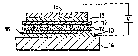
The device of figure 2 comprises an anode electrode layer 10, and a cathode
electrode 11. Located between the electrode layers is a layer 12 of light-
emissive
CA 02354139 2008-11-18
8
materiai. The anode electrode is formed of transparent ITO. The cathode
electrode is formed of calcium. The cathode is sufficientiy thin that It is
not
significantly reflective. Behind the cathode is a iayer 13 of carbon. Wheri a
suitabie voltage Is appiied across the electrodes i'ight is emitted fnorn the
light-
emissive material substantially omnidiredionaAy. Some of the light is emitted
forwards towards the anode and passes directly out of the device through the
anode. Some of the light is emitted backwards towards the cathode. Incident
light that shines on to the display from an extemai source can be absorbed by
the
carbon layer 13. Because this I'ight is absorbed It does not refiect back
towards a
viewer - this can Improve the effect produced by the display, as desaibed in
detail
below.
The device of figure 2 may be formed starting with a commercially-available
glass
sheet coated with ITO. The glass sheet (14 In figure 2) fonns the substrate
for
subsequent deposition steps. The glass sheet could be a sheet of sodalime or
borosiiicate glass of a thickness of, for instance, 1 mm. Instead of. giass
other
materials such as Perspex could be used. The thickness of the ITO coadng is
suitably around 100 to 150nm and the ITO suitably has a sheet resistance of
between 10 and 30 0/0. iOver the ITO anode Is deposited a hole transport or
injectlng layer 15. The hole transport layer is fomied from a solution
containing
PEDOT:PSS with a ratio of PEDOT to PSS of around I to 5. The thiduness of the
hole transport layer is suitabiy around 50nm. The hole transport layer is spin-
coated from soiution and then baked typically at 200 C for 1 hour in a
nitrogen
environment: Then an etecbVuminescent layer 12 'comprising 20% TFB in 5BTF8
Is coated over the hole transpori: layer by spin-coating typIca0y to a
thidcness of
90nm. The term 5BTF8 refers to poy (2,7-(8,9-dt-n-octylfluorene) ("F8*) doped
with 5% poiy-(2,7-(9,8-di-n-octylfluorene)-3,6-benzothiadiazoie) ("FBBT').
Then a
transparent or semitransparent layer of a low work function materiai such as
caicium is' thennaiiy evaporated on to 'the electroluminescent layer In vacuo
at a
base pressure of less than 10-8mbar to form the cathode iayer 11. The
thickness
of this layer is preferabiy greater than around 1nm but less than the
thidcness at
which the caidum layer would be non-transparent - typically around 20nm. Over
CA 02354139 2001-06-08
WO 00/35028 PCT/GB99/04050
9
this layer is deposited by electron beam evaporation a layer 13 of carbon with
a
thickness of between 100 and 500nm at base pressures less than 10"8mbar. On
this layer is deposited by sputter deposition a layer 16 of aluminium with a
thickness of between 100 and 1000nm at base pressures less than 10"8mbar. In
this embodiment the low work function layer 11 is chosen to act as an
efficient
electron injector for injecting electrons into the light-emissive region. The
carbon
layer 13 acts as a light-absorbing layer yet has a conductivity that is low
enough
not to significantly increase the drive voltage of the device. The sputtered
aluminium layer 16 acts as an encapsulant, having a compact morphology with
low pinhole density and small grain size. Contacts can be attached to the
device
(between layers 16 and 10) and it can finally be sealed in epoxy resin for
environmental protection.
Figures 3 and 4 show a multi-pixel display device that makes use of the
principle
described above in connection with the device of figure 2. The device of
figures 3
and 4 comprises a set of parallel anode electrode strips 20 in a common anode
plane and a set of parallel cathode electrode strips 21 in a common cathode
plane
spaced from the anode plane. Between the anode and cathode electrodes is a
light-emissive layer 22. The areas where anode and cathode electrode strips
overlap define pixels of the display device. By using a passive matrix
addressing
scheme individual pixels can be caused to emit light. (The device could
alternatively be configured to allow active matrix or other addressing schemes
to
be used). Figure 4 shows that each cathode electrode comprises three layers:
an
injection layer 75 of a low work function material such as calcium adjacent to
the
emissive layer 22, an intermediate layer 76 of a light-absorbent material such
as
carbon (graphite) and a conduction layer 77 of a highly conductive material
such
as aluminium. Together these make up a cathode plane 81. In general, the
injection layer is suitably of a material that has good properties of
injection into the
light-emissive layer 22; the intermediate layer is suitably of a material that
has
good light-absorbency properties and the conduction layer is of a highly
conductive material. The conduction layer may be significantly thicker than
the
other layers and preferably helps to distribute charge evenly along the
electrode
CA 02354139 2001-06-08
WO 00/35028 PCT/CB99/04050
structure. Where the material chosen for one of the layers can also perform
the
function of another layer then that other layer could be omitted. For
instance, if
the selected light emissive material were one into which good charge injection
could be achieved from carbon then the layer 75 could be omitted, and/or if
the
layers 75 and/or 76 provided adequate conduction then the layer 77 could be
omitted. The light absorbent layer 76 preferably lies between the other two
layers
(where present), in which case it should be electrically conductive, but it
could lie
behind the other two layers Alternatively, or in addition, a light absorbent
layer
covering the whole structure could be provided (layer 29 in figure 4). If that
layer
were of a conductive material such as carbon then an insulating layer 23 could
be
provided to prevent shorting between the cathode strips 21.
The effect of the light-absorbent layer 76 is to absorb light that is incident
on the
display and could otherwise be reflected from the display causing a reduction
in
contrast. This is illustrated by light rays 80 in figure 4, which are absorbed
by
layers 23 and 29. The light-absorbent layer therefore helps to increase
contrast.
The light-absorbent layer may also help to reduce transmission within the
device
itself of light emitted from the light-emissive layer 22. This can help to
increase
contrast by avoiding such light emerging from the device at a location where
it
appears to come from a different pixel from the one from which it was emitted.
One of the contacts from the display driver is applied to the layer 77.
A carbon layer or other non-reflective layer could also be provided in front
of the
light-emissive layer 22 in the lateral spaces between the pixels to further
reduce
reflection of ambient light.
The principles described above in relation to the devices of figures 2 to 4
can
therefore improve contrast between adjacent pixels of a device and improve the
pattern of light emission from a single pixel by reducing emission of more
obliquely angled light and reducing reflection of ambient light.
CA 02354139 2001-06-08
WO 00/35028 PCT/GB99/04050
11
Figure 5 shows another display device. The device of figure 5 comprises an
anode electrode layer 40, and a cathode electrode 41. Located between the
electrode layers is a layer 42 of light-emissive material. The anode electrode
and
the cathode electrode are formed of transparent ITO. Alternatively, for
example,
the electrodes could be formed from a thin layer of a low work function metal
such
as calcium adjacent to an transparent spacing layer formed from a material
such
as ITO, ZnSe, ZnS etc.). When a suitable voltage is applied across the
electrodes
light is emitted from the light-emissive material substantially
omnidirectionally.
Some of the light is emitted forwards towards the anode and passes directly
out of
the device through the anode. Some of the light is emitted backwards towards
the
cathode, through which it passes into a reflection structure indicated
generally at
43. The reflection structure comprises a reflective layer 44 and a transparent
spacing layer 46. The spacing layer lies between the cathode 41 and the
reflective layer 44 and spaces the reflective layer from the light-emissive
region
42. The reflective layer reflects backwardly emitted light forwards so that it
can
pass back through the cathode electrode 41, the light-emissive layer 42 the
anode
electrode 40 and the glass substrate 47 and out of the device (see ray 48).
In figure 5 curve 49 illustrates the form of the optical field and region 50
illustrates
the zone in the device at which electron/hole recombination to generate
photons
is most intense. The equivalent features are illustrated at 60 and 61
respectively
for the device of figure 1. The thickness of the spacing layer in the device
of
figure 5 is ideally chosen so that the plane (or one of the planes) of the
reflective
layer 44 that acts to return backwardly emitted light is spaced from the
emissive
layer by a distance such that at at least one emission frequency of the device
the
peak of the optical mode of the whole reflective arrangement (see curve 49)
coincides with the region of peak electron/hole recombination in the light-
emissive
layer of the device. The effect of this is to arrange that the area of light
generation
in the device is at a more efficient plane of the device of figure 5 than in
the device
of figure 1, by tuning the peak of the optical field (anti-node) to coincide
with the
hole/electron recombination zone of the emissive layer. This optimises (or at
least
partially optimises) the location for efficient light generation for a given
CA 02354139 2001-06-08
WO 00/35028 PCT/GB99/04050
12
wavelength. The wavelength for which the device is optimised preferably is or
is
near the peak intensity emission wavelength. This ideal arrangement calls for
very precise spacing of the respective layers; however, considerable benefits
can
be gained by arranging the layers approximately or substantially in that way.
The device of figure 5 may be formed by a similar route to that described
above
for the device of figure 2 up to the formation of the cathode electrode. Then
for
the device of figure 5 the spacing layer 46 is formed by depositing ITO, ZnSe,
ZnS
or the like to the required thickness, preferably on top of a thin layer of a
low work-
function metal such as calcium. Over the ITO spacing layer the reflective
layer 44
is formed from reflective material such as aluminium. In an alternative
embodiment a conducting dielectric stack next to or spaced from the cathode
could be used as the reflector. Such a stack could be formed, for example, of
alternating layers of ITO and NiO.
In another alternative embodiment, one of the electrodes could be formed of a
reflectivity influencing material. The anode or the cathode could be
reflective or
non-reflective (light-absorbent). This could be achieved by choosing a
material
with the desired reflectivity properties and the preferred charge conduction
and
injection properties. An electrically suitably material could be treated (e.g.
by
surface treatment or incorporation into it of a reflectivity influencing
additive) to
obtain the desired reflectivity properties.
One specific example is for the rear electrode (the one furthest from a
viewer) to
be non-reflective. In a device arranged generally as those in figures 1 to 5,
this
calls for a non-reflective cathode. (in other devices the anode may be the
rear
electrode). One suitable material for a reflective or non-reflective cathode
is
LiF:Al. When the Al component of a LiF:AI film is greater than 50% the LiF:Al
films are reflective. When the Al component is between 50% and 30% the films
are non-reflective. When the Al component is <30% the films are semi-
transparent but also have very high resistivities. Therefore, in the range
50:50 to
70:30 LiF:AI LiF/Al films are useful for making a black (non-reflective)
cathode.
CA 02354139 2001-06-08
WO 00/35028 PCT/GB99/04050
13
An example device having a non-reflective rear electrode (in this case the
cathode) can be manufactured as follows. On to a glass substrate a 150nm thick
layer of ITO is deposited to act as an anode electrode. Then a 50nm thick
layer of
PEDOT/PSS is deposited to act as a hole transport layer. Over that an 80nm
thick layer of a polyfluorene based electroluminescent polymer is formed.
Finally
the non-reflective cathode layer is deposited as a 200nm thick layer of co-
evaporated LiF and Al, with the LiF:AI evaporation rates being 60:40. On top
of
this layer a 400nm thick Al layer is deposited. In varying this specific
design of
device it should be noted that the range of potential thickness for the LiF:Ai
layer
depends on the composition since the greater the proportion of LiF in the
layer the
more transparent the layer becomes. For layers of composition 60:40 LiF:AI
200nm is just thick enough. A suitable range of thickness is from 50 to
1000nm.
Alternative non-reflective cathode materials include generally fluorides and
oxides
of low work function metals such as Li, Ca, Mg, Cs, preferably together with
an
inherently highly conductive metal such as Al or Cu (although in some
situations
Cu may be less preferred because of its tendency to quench polymers'
electroluminescence). Specific examples include CsF, MgF, CaF, LiO, CaO,
which could be co-evaporated with Al or sputtered from a composite target
including Al. The required ratios of the conductor (Al) with the insulating
fluorides
and oxides can easily be determined by experimentation in each case but might
be expected to be similar to those discussed for the LiF:AI system above.
Another alternative route to a low reflectivity or non-reflective or cathode
is to co-
evaporate or sputter a low work function material with carbon. Examples
include
the low work function metals Ca, Li etc and also the fluorides and oxides
listed
above.
Figure 6 is a plan view and figure 7 a cross-sectional view of another
alternative
device. The device comprises an anode electrode 60, a hole transport layer 62,
a
cathode electrode 63, a light-emissive layer 64 and a distributed Bragg
reflector
(DBR) layer 65. The DBR is located on the non-viewing side of the light-
emissive
CA 02354139 2001-06-08
WO 00/35028 PCT/GB99/04050
14
layer. The bulk (66) of the cathode 63 is located on the non-viewing side of
the
DBR. To allow charge to pass from the bulk of the cathode to the light-
emissive
region cathode vias 67 are provided through the DBR. The vias occupy a
relatively small proportion of the area of the device: for example around 15%
to
5%. To even out charge injection into the emissive layer a further layer 68 of
the
cathode which is sufficiently thin to be transparent is provided between the
DBR
and the light-emitting region. If the DBR were conductive, or the vias were
closely spaced, or uniformity could otherwise be achieved then the layer 68
could
be omitted. The mesh-like arrangement of vias (see figure 6) could be formed
by
means of deposition through a shadow mask.
A DBR comprises of a stack of regularly alternating higher- and lower-
refractive
index dielectrics (light transmissive materials) fabricated to fulfil the
Bragg
condition for reflection at particular wavelengths. This occurs when the
optical
path of the periodicity in the dielectric stack corresponds to half a
wavelength, and
the reflectivity is further optimised when the DBR stack obeys the following
equation:
'/z nid, + n2d2,
where n,, n2 are the respective refractive indices; d,, d2 are the
corresponding
component film thicknesses in the DBR; and X is the desired reflection
wavelength. Figure 8 shows the reflectivity of a DBR against wavelength, the
reflectivity peaking at that optimum and being much lower for other
wavelengths.
In the device of figures 6 and 7 the DBR is arranged so that the emission
wavelength of the light-emissive layer (or its principal emission wavelength)
lies
within the reflectivity peak of the DBR, and most preferably at or near the
maximum reflectivity of the DBR. The effect of this is that the DBR can act to
increase the contrast of the device without significantly reducing its
efficiency.
Light emitted rearwards from the light-emissive layer is reflected efficiently
(e.g.
with around 95% to 100% reflectivity) back towards a viewer by the DBR.
Incident
light that is not at or near the emission wavelength of the light-emitting
layer, and
therefore not within the reflectivity peak of the DBR, is reflected much less
(e.g.
CA 02354139 2001-06-08
WO 00/35028 PCT/GB99/04050
only 5% to 10%) and tends to be absorbed by the DBR, improving the contrast of
the device. The peaky reflectivity of the DBR may also serve to enhance colour
purity of the emission from the device.
The vias may be reflective to a range of wavelengths, so it is preferred to
minimise the area occupied by the vias, for example to below 15% and
preferably
below 10%.
Some variations on the devices described above will now be described. In any
of
the devices one or more charge transport layers (e.g. layers 15, 70, 71) may
be
formed between the light-emissive layer and either or both of the electrodes
to
assist charge transport between the respective electrode and the light-
emissive
layer and/or to resist charge transport in the opposite direction. The
principles
described above could be applied to other types of organic or inorganic
display
devices. One specific alternative example is the class of display devices that
use
sublimed molecular films for light emission, as described for example in
"Organic
Electroluminescent Diodes", C. W. Tang and S. A. VanSlyke, Appl. Phys. Left.
51,
913-915 (1987). The locations of the electrodes could be reversed so that the
cathode is located at the front of the display (closest to the viewer) and the
anode
is at the back. Other materials or classes of materials could be used instead
of
those mentioned above, although this may impair performance of the devices.
The applicant draws attention to the fact that the present invention may
include
any feature or combination of features disclosed herein either implicitly or
explicitly or any generalisation thereof, without limitation to the scope of
any of the
present claims. In view of the foregoing description it will be evident to a
person
skilled in the art that various modifications may be made within the scope of
the
invention.