Note: Descriptions are shown in the official language in which they were submitted.
CA 02354434 2001-07-26
Process and Apparatus for the Printing of Digital Image Information
Field of the Invention
The invention relates to processes and apparatus for the pixel by pixel
printing of
digital image information onto a planar picture carrier in a printing device
by way of a
movable printing head.
Background Art
The manufacture of physical prints of digital originals is increasingly
carried out
by a printing process, whereby inkjet printers are normally used. A high-
performance
inkjet printer which is typically used for these purposes is described in EP-A
1 009 158.
Borderless pictures are often desired by the photographic industry. However,
when inkjet printers are used, this is associated with problems to which a
satisfactory
solution has not yet been found. In an often applied method for the
manufacture of
borderless pictures, a picture format to be printed is selected which is
smaller than the
picture carrier format, so that pictures with an unprinted border are
produced, and the
unprinted borders are cut off. This method requires relatively expensive
cutting
operations and additionally produces undesired picture carrier waste. In
another common
method, the picture format to be printed is selected larger than the picture
carrier format.
However, this wastes printing ink and furthermore, there is a danger of
soiling by the
printing inks applied outside the picture carrier, and the removal of the
printing inks
applied outside the picture carrier is relatively expensive.
It is a further danger with inkjet printers the individual nozzles of the
printing
heads may clogg. Although it is possible to maintain the printing nozzles
clear and
thereby functional by frequent flushing or other cleaning, this results in a
relatively high
printing ink consumption. Furthermore, the printing heads become prematurely
worn by
the frequent cleaning and the printing process must be interrupted relatively
frequently.
It is also known to print special test patterns from time to time, by way of
which it can be
determined visually or by photoelectric scanning and analysis of the scanning
signals
whether and, if desired, which printing nozzles have failed. A visual
inspection is
unsuited for high-performance printers, because of the danger of producing
large amounts
1
CA 02354434 2001-07-26
of waste. The known automatic systems with photoelectric scanning are only
adapted for
relatively large print dots (ink droplets) and for a relatively small number
of inkjets and
are therefore not suited for modern high-performance printers with very high-
resolution
and a correspondingly large number of very fine ink nozzles.
High-performance inkjet printers include a plurality of print heads, which
must be
exactly mutually oriented in a costly manner, since incorrect adjustments lead
to visible
disturbances in the printed image. Visible disturbances are further caused by
incorrect
location of printing dots from individual printing nozzles and by different
sizes of
printing dots from individual printing nozzles. Although the latter can be
averaged out
(corrected or compensated for) to some degree by multiple printing passes,
that
significantly reduces the printing speed.
A further problem of inkjet printers is to correct color reproduction, which
is
subject to variations due to changes in the picture carrier material, the
printing inks, the
printing head characteristics and environmental conditions such as temperature
and
humidity. Although an exact color reproduction can be achieved by limiting the
number
of picture carrier materials used (printing media, printing substrates) and by
carefully
profiling each combination of printing modes and picture carrier materials,
this is
achieved at the cost lost flexibility with respect to the usable picture
carrier materials and
printing inks. When a new picture carrier material is added, a new profile
must first be
created at additional expense and by employing specially trained personnel.
It is now a primary object of the present invention to solve the problem of
manufacturing borderless pictures in a simple and economic manner. A waste of
picture
carrier material and printing ink is thereby to be particularly avoided. It is
a further
object of the invention to combine the solution of the problem for the
manufacture of
borderless pictures with the provision of the prerequisites for getting the
other above
mentioned difficulties with inkjet and comparable printers under control.
This object of the invention is achieved by the printing process in accordance
with
the invention , wherein the borders of the picture carrier are detected,
preferably by way
of a photoelectric sensor, and the printing of the pixels of the digital
picture which lie
beyond the borders of the picture carrier is suppressed. When the borders are
detected
with sufficient precicion, a borderless printing is possible in this manner
without wasting
2
CA 02354434 2001-07-26
printing ink. It is thereby understood, that the format of the picture to be
printed should
be selected marginally larger than the format of the picture carrier.
When the photoelectric sensor is suitably constructed, it can also be used for
the
photoelectric scanning or measurement of co-printed print head test patterns,
in
accordance with a further aspect of the invention. The functional condition of
the print
head or print heads of the printing apparatus can then be determined by
analyzing with
suitable algorithms the measured data produced by the sensor, and
corresponding
measures can then be initiated. The production of waste can be reliably
prevented in this
manner.
When the photoelectric sensor is adapted for densiometric or colorimetric
measurement tasks, it can also be used for the measuring of co-printed color
test patterns,
according to a further aspect of the invention. In this manner, changes in the
color
reproduction quality can be recognized in time by measurement technology and
corrected
by suitable measures.
The most basic and general idea of the present invention consists in the use
of a
single, specially constructed multifunctional sensor for a series of very
different
photoelectric measurement tasks. All the above described problems with inkjet
printers
and comparable printers can be addressed in a simple manner by way of this
special
multifunctional sensor (and a corresponding control or analysis arrangement
for the
measured data produced by the sensor).
Brief Description of the Drawings
The invention will be described in the following with reference to the
drawings,
wherein
Figure 1 shows a principle schematic of the preferred embodiment of the
printing
device in accordance with the invention;
Figure 2 shows an exemplary embodiment of a photoelectric multifunctional
sensor provided in the printing device in accordance with the invention;
Figure 2a is a schematic view of the inspection region of the sensor shown in
Figure 2;
Figure 3 is a schematic illustration of the progression of the position of the
CA 02354434 2001-07-26
borders of a picture carrier;
Figure 4 is a function sketch for the illustration of the detection of the
borders of
the picture carrier;
Figure 5 is a schematic illustration of a mask;
Figure 6 is a schematic illustration of masked image information;
Figures 7 to 9 show typical test patterns for control of the functional
condition of
the printing heads and the color reproduction quality; and
Figures 10 to 12 show the typical measured data diagrams belonging to the
situations shown in Figures 7 to 9.
Detailed Description of the Preferred Embodiment
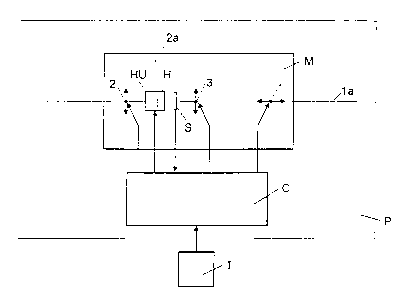
The printing apparatus referred to in Figure 4 in its entirety as P includes
in a
housing or frame (not illustrated) an ink jet printing unit HU which normally
consists of
several inkjet print heads H, which are fed by not illustrated reservoirs for
printing inks of
different colors. Further provided in the housing are positioning means l,
illustrated only
symbolically by a double arrow, for a sheet or web shaped picture carrier M to
be printed
(normally paper of suitable quality). The positioning means provide for the
displacement
of the picture carrier M in or through the printing device P in a defined
matter along a
displacement path 1 a relative to the printing unit HU or relative to the
print heads H,
whereby a control C controls the movements in a manner generally known.
Furthermore,
advancing means 2 controlled by the control C, which are also only
symbolically
indicated by a double arrow, are provided in the printing device P, by which
the printing
head unit HU or the print heads H are adjustable along a displacement path 2a
extending
essentially transverse to the path of moment 1 a of the picture carrier.
The picture carrier M and the printing heads H are thereby movable relative to
one another in a generally known manner in two orthogonal directions, so that
each print
head H can be positioned under the control of the control C at any desired
location of the
picture carrier M. The print heads H of the printing head unit HU are
controlled by the
control C and print on the picture carrier M the digital image information I
wish was fed
to the control C by an external computer or like. The image information I is
printed pixel
by pixel onto the picture carrier M in a manner generally known and in the
form of fine
4
CA 02354434 2001-07-26
ink droplets.
In the practical embodiment, the printing device can be constructed, for
example,
as a drum recorder as described in all detail in EP-A 1009 158. Such a drum
recorder
typically includes a rotating clamping drum for the recording medium (the
picture carrier)
and a printing unit which is stationary relative to the rotational movement of
the clamping
drum, which consists of 1 or more print heads displaceable parallel to the
axis. The
whole surface of the image carrier held on the clamping drum is passed over by
rotation
of the clamping drum on the one hand and displacement of the printing heads
parallel to
the axis of the tensioning dmm on the other hand. The rotational or
circumferential
direction of the tensioning drum corresponds to the displacement path la in
Figure 1 and
the direction of the clamping drum axis corresponds to the displacement track
2a in
Figure 1.
Up to this point, the printing apparatus in accordance with the invention
fully and
wholly corresponds to conventional inkjet printing devices and, therefore,
does not
require any further explanation for the person skilled in the art.
According to the most preferred aspect of the present invention, the printing
device is equipped with a photoelectric multifunctional sensor S which can be
moved
back and forth parallel to the print heads H over the whole width of the
picture carrier M
by way of a drive means 3 also controlled by the control C and only
symbolically
identified by a double arrow. Alternatively, the sensor S can also be
mechanically
connected with the print head unit HU and positioned for movement therewith.
The
sensor S photoelectrically scans the picture carrier M positioned thereunder,
whereby the
scanning signals produced by the sensor S are processed by the control C in a
manner
which will be described later and analyzed for the process in accordance with
the
invention.
The principal construction of the photoelectric sensor S is apparent from
Figure 2.
It is constructed as a color enabled remissions sensor of high local
resolution and includes
essentially a light source in the form of several light emitting diodes 11, a
capturing
optics 12, and a photoelectric converter 13, which itself is made of a linear
or two-
dimensional field of photoelectric converter elements. The light source
exposes, or the
light emitting diodes 11 expose the picture carrier M under the sensor S to
measuring
CA 02354434 2001-07-26
light essentially at an angle of 45°.
The measuring light remitted from the surface of the picture carrier M is
captured
by the capturing optics 12 under 90 ° and directed onto the
photoelectric converter 13,
which converts it into corresponding electric signals.
For improvement of the contrast, the light emitting diodes 11 preferably emit
the
colors complementary to the printing inks used, i.e. typically red, blue or
green. Instead
of the colored light emitting diodes, sources of white light can be provided
in
combination with suitable color filters.
The capturing optics 12 is preferably formed by a field of gradient-index
glass
fibers, but can also be realized as a conventional object lens.
The photoelectric converter 13 is preferably realized in CCD or CMOS
technology and has a relatively high linear resolution of, for example 10 ~.
The length of
the converter can be, for example, 20-30 mm, which corresponds to a number of
2000 to
3000 converter elements [pixels] per line. The converter 13 can include one or
more
lines of converter elements and is connected to the control C by way of a
driver electronic
13a. The electric signals produced by the individual converter elements and
corresponding to the measuring light received are transmitted in a known
manner by the
driver electronic 13a to the control C.
Color enabled photoelectric scanning devices (sensors) which operate pixel by
pixel with photoelectric converter elements fields (CCD arrays and the like)
as well as the
driver electronics and signal processors required therefor are known in the
color
measuring technology from digital cameras and therefore do not require any
further
explanation for the person skilled in the art.
The capturing optics 12 and the converter 13 can be realized as an analog or
digital camera, for example, which already includes the driver and signal
processing
electronic 13a for the photoelectric converter elements.
The sensor S photoelectrically scans the picture carrier pixel by pixel
respectively
in a narrow, rectangular inspection region with high local resolution, whereby
densiometric color measurements are also possible with the use of colored
measuring
light. Such an inspection region is illustrated in Figure 2a and referred to
by reference
number 15. The length of a typical inspection region is about 20-30 mm, the
width about
CA 02354434 2001-07-26
p, to several mm. The linear local resolution in longitudinal direction is
typically
about 10 ~.. Of course, the dimensions of the inspection region can also be
differently
selected without departing from the framework of the present invention.
In the normal case, the sensor S is oriented such that the longitudinal extent
of the
inspection region 15 is parallel to the displacement path of the print heads H
or the sensor
S itself. However, the sensor S can also be positioned in such a way that the
longer side
of the inspection region I ~ is rotated an angle of preferably 45 ° to
the displacement path
of the print heads H.
Because of its special construction according to the invention, the sensor S
can be
used for all required measurement tasks, in order to solve the above mentioned
problems
with inkjet printers during printing.
According to a first aspect of the invention, the sensor is used for capturing
the
exact local progression of the borders of the picture carrier M. The
information obtained
on the location of the borders is thereby used for blocking out of the image
elements
(pixels) of the digital image information I to be printed which are located
beyond the
borders, so that image elements which are located outside the borders are not
printed.
This is further described in the following, whereby it is assumed for reasons
of simplicity
that the picture carrier M is in the form of any web material so that
generally only the two
opposite lateral borders of the picture carrier need be detected. The case of
picture
carriers in sheet form or the capturing of borders extending transverse to the
direction of
movement of the picture carrier M is dealt with further below.
As illustrated strongly exaggerated in Figure 3, the location of the lateral
borders
R~ and RZ of the picture carrier M varies within certain limits relative to a
stationary
coordinate system in the printing device, for example, because inexactness of
the
positioning means 1 which are hard to prevent in practice and possibly also
because of
variations in the width of the picture carrier itself. Since the movement of
the print heads
and therefore the location of the printed picture is also with respect to this
stationary
cordinate system, more or less large marginal regions of the image information
or images
I to be printed as identified by rectangles come to lie outside the picture
carrier M. The
image regions lying outside the borders of the picture carrier M are
identified as Ie in
Figure 3. In order to be able to eliminate in accordance with the invention
these picture
CA 02354434 2001-07-26
regions Ie, or the pixels forming them, which means being able to suppress
these picture
elements, the local position of the two lateral borders R~ and Rz of the
picture carrier
must be known at each point along the longitudinal extent of the picture
carrier.
Figure 4 schematically illustrates how the capturing of the location of the
lateral
borders of the image carrier M takes place in principle by way of the sensor
S. One
coordinate axis of the already mentioned stationary coordinate system which
extends
parallel to the direction of movement 2a of the sensor is called x, the axis a
defines the
level or signal strength of the electric signals produced by the individual
converter
elements of the sensor S, and corresponding to the intensity of the measuring
light
impinging thereon. The two coordinate axes p define the relative location
(pixel
coordinates) of the individual converter elements of the sensor thereon.
The sensor is transversely moved by the control C across the width of the
picture
carrier M into two positions indicated S' and S" in Figure 4 having the local
coordinates
x' and x", in which it or the inspection region captured by it is located over
the borders Rl
and RZ of the picture carrier M. At those positions, the converter elements
receiving
measuring light from within regions inward from the border of the picture
carrier M
deliver a high signal level, while the remaining converter elements do not
receive
measuring light and therefore produce a low signal level. The converter
elements which
fall within the level changes are determined by the control C by suitable
analysis of the
measurement signals and their relative locations p' and p" (pixel coordinates)
on the
sensor are determined. The pixel coordinates p' and p" together with the
location
coordinates x' and x" of the sensor provide the exact positions of the two
borders Rl and
RZ of the picture carrier M. The picture carrier M is now advanced by a path
increment
in direction of the displacement path la and the whole process repeated until
the local
progression of the two borders has been captured over the whole length of the
image
carrier M.
An alternative approach consists in that first the complete local progression
of
only one border Rl is captured and subsequently the path of the other border
R2. This
approach is advantageous especially when the printing device P is constructed
as a drum
recorder according to EP-A 1 009 158. The sensor is thereby first positioned
over one
border of the image carrier fastened to the clamping drum and then the
clamping drum
s
CA 02354434 2001-07-26
rotated once through 360 °. Subsequently, the sensor is positioned over
the other border
and the tensioning drum is again the rotated through 360 °. During each
rotation of the
clamping drum, the local position of respectively one of the two lateral
borders along the
whole fastened image carrier is determined and stored.
By way of the stored local progression of the borders of the image carrier M,
a
mask is calculated in the control C and positioned over the image information
I to be
printed. The mask identities all those pixels I~ of the image information I to
be printed,
which are located outside the previously captured borders Rl and RZ of the
picture carrier
M. Superposing the mask over the image information I is carried out in a way
so that the
digital color values of the affected pixels I~ are set at "transparent" so
that those pixels I
are not printed. Such a mask is schematically illustrated in Figure 5 and
referred to as 16.
Figure 6 schematically illustrates the printable image information I'
remaining after
superposition of the image information I with the mask 16.
The above described approaches capture the borders of the image carrier M
before
the printing of the image information I. This presumes that the image carrier
M can be
reproducably positioned to in the printing device with sufficient precision.
If this is not
possible due to the construction of the printing device, the capturing of the
borders and
the calculation and superposition of the mask must be carried out "on-the-fly"
line by line
during the printing operation. The local position of one border of the image
carrier M is
thereby captured for each printing line defined by the transverse movement of
the print
heads H along the displacement path 2a and the position of the picture carrier
M along
the displacement path 1 a, and a partial mask is calculated therefrom and
superposed onto
the image information I (for this printing line), so that pixels (of this
printing line) which
are located outside of this border not printed. The print heads H together
with the sensor
S are then advanced normally and the line of image information is printed. As
soon as the
opposite border of the image carrier enters the inspection region of the
sensor S, the local
position of this opposite border is captured and a second partial mask
calculated
therefrom and superposed onto the image information (of this printing line) so
that the
pixels (of this printing line) which are located outside this border are also
not printed.
The process is subsequently repeated in the opposite direction and so on until
the whole
image information is printed.
9
CA 02354434 2001-07-26
As already mentioned, borders extending transverse to the advancement
direction
1 a of the picture carrier M can also be captured with the sensor S. In the
normal
orientation of the sensor S orthogonally to the advancement direction 1 a, the
signal levels
of practically all converter elements of the sensor S simultaneously change
during
passage over a transversely extending border. The local position of the
respective border
can be determined from the temporal or three-dimensional information of this
level
change and the mask calculated therefrom (in combination with the location
information
of the two lateral borders). Analog to the capturing of the two lateral
borders, the
preceding and subsequent borders of the picture carrier can also be captured
"on-the-fly",
when a capturing before printing is not possible, for example, because of the
mechanical
parameters of the printing device. When the sensor S is positioned rotated
relative to the
displacement path 2a of the print heads H at a specific angle, especially 45
°, the
capturing of the preceding or following borders can be carried out similar to
the manner
described in connection with Figure 4.
Of course, the control C can also be constructed to interrupt the printing
process
or not even start it and to output a corresponding warning, if the captured
borders of the
picture carrier are located outside a preselected tolerance range.
According to a second aspect of the present invention, the sensor S is also
used
for the measurement of from time to time (co-) printed test patterns, by way
of which the
functional condition and the mutual adjustment of the print heads H can be
automatically
tested.
Figures 7-10 schematically describe the approach for the recognition of print
nozzles of the print heads H which have failed, for example, because of
clogging. A test
pattern 10 is printed therefor, which is created by single or multiple
activation of all
nozzles of one color of respectively one print head H during advancement of
the picture
carrier. Each functioning nozzle thereby prints a short line, while missing
lines are
caused by clogged nozzles. To prevent ambiguities during this scanning, at
least one of
the lines of the test pattern is longer (or shorter) than the others. In
contrast to those test
patterns used for visual inspection, the test pattern 10 can be maintained
very small and
therefore can be positioned between the pictures to be printed or close to the
border of the
picture career.
CA 02354434 2001-07-26
The test pattern 10 is singly or multiply scanned with-the sensor S transverse
to
the lines of the test pattern. During each scanning, the typical signal trace
as partially
illustrated in Figure 10 is created by way of the individual converter
elements (pixel
coordinate p) of the sensor S. Each line of the test pattern 10 actually
present creates a
negative signal peak, while the corresponding signal peak is missing when the
line is
missing because of nozzle failure. The control C can determine from the signal
trace by
counting of the peaks and identification of the missing peaks whether and
possibly which
nozzles of the respective printing head H have failed. When the failure of one
or more
printing nozzles has been recognized in this way, it is automatically decided
by way of a
preselected criterion, whether the printing process must be interrupted and
maintenance
(cleaning, replacement) of the print head requested or initiated or whether
the printing
process can be continued with the remaining functional printing nozzles.
Because, when
not too many printing nozzles have failed, it is possible to divide the tasks
of the failed
nozzles over the remaining functional nozzles in a known manner. This approach
is
generally known as software nozzle replacement. The cleaning of the print
heads H can
also be carried out, possibly with the help of known cleaning agents and
methods, under
the control of the control C.
Figures 8 and 11 schematically illustrate the procedure for the testing of the
mutual adjustment of the print heads upon detection of incorrect locations of
printed dots
of individual print nozzles. A test pattern 20 is printed which is structured
similar to the
test pattern 10 but with the distinction that it is printed with more than one
print head H
(H 1 and H 2 in the illustrated example). As is apparent, in this example the
two printing
heads H1 and H 2 are incorrectly adjusted, since the two lines 21 and 22 of
the test
pattern 20 are too close to one another. Furthermore, one of the nozzles of
the print head
H2 produces an incorrect positioning for the print dots produced thereby (line
23). The
typical signal trace over the pixel coordinate p generated upon scanning of
the test pattern
20 is illustrated in Figure 11 (partially). The control C again analyzes these
signal traces.
Thereby not only the number of lines present his determined, but also their
relative
positions (pixel coordinate). The positions of the individual lines are
compared with
preset positions. Upon the occurrence of deviations, is automatically decided
whether or
not a correction measure is required. The correction measure can consist on
the one hand
11
CA 02354434 2001-07-26
in a mechanical readjustment of the print heads H or in the use of a software
correction,
which can compensate for the incorrect adjustment of the printing heads and
also the
incorrect locations of the printing dots produced by the nozzles. The
mechanical
readjustment of the printing heads H can possibly also be carried out
automatically by the
control C by way of adjustment means. The adjustment means can be, for
example,
motor driven set screws or other actuators for the adjustment of the print
heads.
According to a further aspect of the present invention, the sensor S is also
used for
the measuring of color test patterns, by way of which the color reproduction
quality of the
print device can be tested and corrected if necessary. Figures 9 and 12
schematically
illustrate the approach required therefor.
A color test pattern 30 is printed, which consists of a number of (9 in the
illustrated example) small color test fields of different colors. Typically,
the colors of the
printing inks used (cyan, yellow, magenta, black) and the edited primary
colors (red,
blue, green) as well as black and some gray shades are used. The color
measurement
fields of the color test pattern are scanned with the sensor S, whereby each
color
measurement fields is measured with each measurement light color. Figure 12
shows a
typical signal trace over the pixel coordinate p for one scanning passage
(three captured
color measurement fields with one measurement light color). The intensity
values
determined for the individual color measurement fields for each measurement
light color
are compared to reference values previously stored in the control C and the
deviations
determined. When the deviations fall outside a preselected tolerance range, a
correction
measure is initiated.
A suitable correction measure can be, for example, the adjustment or new
generation of the apparatus profile of the printing device P (printer output
profile) and the
subsequent carrying out of all printing processes with the new profile.
Methods and
apparatus for the generation of apparatus profiles are described in the color
management
literature and are known to the person skilled in the art.
An alternative possibility for an automatic correction measure consists in
influencing the size of the ink droplets produced by the nozzles of the print
heads H by
corresponding adjustment of the driver voltages applied to the nozzles. By
changing the
droplet sizes, the color reproduction characteristic of the printing device
can be
12
CA 02354434 2001-07-26
automatically controlled within certain limits.
It is required for this approach that the color test pattern 30 include
halftone color
test fields in the pure colors of the colored inks used, i.e. color test
fields in the colors of
the printing inks with a respective areal coverage of less than 100 percent.
These
halftone color test fields are measured in the manner described by way of the
sensor S
and their color densities are determined and compared with reference values.
When the
color density measured for a printing ink falls outside a preselected
tolerance range, the
droplet size for this color ink is, depending on the deviations, increased or
reduced by
way of the control C. In this manner, the color reproduction quality of the
printing device
can be automatically maintained constant within certain limits.
13