Note: Descriptions are shown in the official language in which they were submitted.
CA 02355171 2008-11-05
METHOD OF APPLYING A PHASE CHANGE
THERMAL INTERFACE MATERIAL
BACKGROUND OF THE INVENTION
The present invention relates broadly to a phase change, thermal interface
material which
is interposable between, for example, the heat transfer surfaces of a heat-
generating, electronic
component and a thermal dissipation member, such'as a heat sink or circuit
board, for the
conductive cooling of the electronic component. More particularly, the
invention relates to the
spray application of such material to the heat transfer surface of the
component or dissipation
member to achieve a relatively thin film thickness thereon which minimizes the
thermal
impedance between the component and dissipation member.
Circuit designs for modern electronic devices such as televisions, radios,
computers,
medical instruments, business machines, communications equipment, and the like
have become
increasingly complex. For example, integrated circuits have been manufactured
for these and
other devices which contain the equivalent of hundreds of thousands of
transistors. Although the
complexity of the designs has increased, the size of the devices has continued
to shrink with
improvements in the ability to manufacture smaller electronic components and
to pack more of
these components in an ever smaller area.
As electronic components have become smaller and more densely packed on
integrated
boards and chips, designers and manufacturers now are faced with the challenge
of how to
dissipate the heat which is ohmicly or otherwise generated by these
components. Indeed, it is
well known that many electronic components, and especially power semiconductor
components
such as transistors and microprocessors, are more prone to failure or
malfunction at high
temperatures. Thus, the ability to dissipate heat often is a limiting factor
on the performance of
the component.
Electronic components within integrated circuit traditionally have been cooled
via forced
or convective circulation of air within the housing of the device. In this
regard, cooling fins have
CA 02355171 2001-06-13
WO 00/36893 PCT/US99/20750
2
been provided as an integral part of the component package or as separately
attached thereto for
increasing the surface area of the package exposed to convectively-developed
air currents.
Electric fans additionally have been employed to increase the volume of air
which is circulated
within the housing. For high power circuits and the smaller but more densely
packed circuits
typical of current electronic designs, however, simple air circulation often
has been found to be
insufficient to adequately cool the circuit components.
Heat dissipation beyond that which is attainable by simple air circulation may
be effected
by the direct mounting of the electronic component to a thermal dissipation
member such as a
"cold plate" or other heat sink. The heat sink may be a dedicated, thermally-
conductive metal
plate, or simply the chassis or circuit board of the device. However, beyond
the normal
temperature gradients between the electronic component and the heat sink, an
appreciable
temperature gradient is deveioped as a thermal interfacial impedance or
contact resistance at the
interface between the bodies.
That is, and as is described in U.S. Patent No. 4,869,954, the faying thermal
interface
surfaces of the component and heat sink typically are irregular, either on a
gross or a microscopic
scale. When the interfaces surfaces are mated, pockets or void spaces are
developed
therebetween in which air may become entrapped. These pockets reduce the
overall surface area
contact within the interface which, in turn, reduces the heat transfer area
and the overall
efficiency of the heat transfer through the interface. Moreover, as it is well
known that air is a
relatively poor thermal conductor, the presence of air pockets within the
interface reduces the rate
of thermal transfer through the interface.
To improve the heat transfer efficiency tlirough the interface, a layer of a
thermally-
conductive, electrically-insulating material typically is interposed between
the heat sink and
electronic component to fill in any surface irregularities and eliminate air
pockets. Initially
employed for this purpose were materials such as silicone grease or wax filled
with a thermally-
conductive filler such as aluminum oxide. Such materials usually are semi-
liquid or solid at
normal room temperature, but may liquefy or soften at elevated temperatures to
flow and better
conform to the irregularities of the interface surfaces.
For example, U.S. Patent Nos. 4,473,113 and 4,299,715 disclose a wax-like,
heat-
conducting material which is combined with another heat-conducting material,
such as a
beryllium, zinc, or aluminum oxide powder, to form a mixture for completing a
thermally-
CA 02355171 2001-06-13
WO 00/36893 PCT/US99/20750
3
conductive path from a heated element to a heat sink. A preferred wax-like
material is a mixture
of ordinary petroleum jelly and a natural or synthetic wax, such as beeswax,
palm wax, or
mineral wax, which mixture melts or becomes plastic at a temperature above
normal room
temperature. The material can be excoriated or ablated by marking or rubbing,
and adheres to the
surface on which it was rubbed. In this regard, the material may be shaped
into a rod, bar, or
other extensible form which may be carried in a pencil-like dispenser for
application.
U.S. Patent No. 3,928,907 discloses a method of optimizing thermal conduction
between
a heat source such as a transistor, and a porous, laminated wire mesh heat
sink by providing an
interface mounting pad of a high thermal conductivity metal. The pad is built
up by flame
spraying molten metai particles of copper onto the porous metal surface.
U.S. Patent No. 4,466,483 discloses a thermally-conductive, electrically-
insulating
gasket. The gasket includes a web or tape which is formed of a material which
can be
impregnated or loaded with an electrically-insulating, heat conducting
material. The tape or web
functions as a vehicle for holding the meltable material and heat conducting
ingredient, if any, in
a gasket-like form. For example, a central layer of a solid plastic material
may be provided, both
sides of which are coated with a meltable mixture of wax, zinc oxide, and a
fire retardant.
U.S. Patent No. 4,473,113 discloses a thermally-conductive, electrically-
insulating sheet
for application to the surface of an electronic apparatus. The sheet is
provided as having a
coating on each side thereof a material which changes state from a solid to a
liquid within the
operating temperature range of the electronic apparatus. The material may be
formulated as a
meltable mixture of wax and zinc oxide.
U.S. Patent No. 4,764,845 discloses a thermally-cooled electronic assembly
which
includes a housing containing electronic components. A heat sink material
fills the liousing in
direct contact with the electronic components for conducting heat therefrom.
The heat sink
material comprises a paste-like mixture of particulate microcrystalline
material such as diamond,
boron nitride, or sapphire, and a filler material such as a fluorocarbon or
paraffin.
U.S. Patent Nos. 5,250,209 and 5,167,851 disclose a water-soluble, thermally-
conductive
grease useful for the thermal coupling of electronic chips and heat sinks. The
thixotropic,
dielectric grease comprises a hydrophilic liquid polymer carrier and a
microparticulate,
thermally-conductive filler.
CA 02355171 2001-06-13
WO 00/36893 PCT/US99/20750
4
The greases and waxes of the aforementioned types heretofore known in the art,
however, generally are not self-supporting or otherwise form stable at room
temperature and are
considered to be messy to apply to the interface surface of the heat sink or
electronic component.
To provide these materials in the form of a film which often is preferred for
ease of handling, a
substrate, web, or other carrier must be provided which introduces another
interface layer in or
between which additional air pockets may be formed. Moreover, use of such
materials typically
involves hand application or lay-up by the electronics assembler which
increases manufacturing
costs.
Alternatively, another approach is to substitute a cured, sheet-like material
or pad for the
silicone grease or wax material. Such materials may be compounded as
containing one or more
thermally-conductive particulate fillers dispersed within a polymeric binder,
and may be provided
in the form of cured sheets, tapes, pads, or films. Typical binder materials
include silicones,
urethanes, thermoplastic rubbers, and other elastomers, with typical fillers
including aluminum
oxide, magnesium oxide, zinc oxide, boron nitride, and aluminum nitride.
Exemplary of the aforesaid interface materials is an alumina or boron nitride-
filled
silicone or urethane elastomer which is marketed under the name CHO-THERM by
the
Chomerics Division of Parker-Hannifin Corp., 77 Dragon Court, Woburn, MA
01888.
Additionally, U.S. Patent No. 4,869,954 discloses a cured, form-stable, sheet-
like, thermally-
conductive material for transferring thermal energy. The material is formed of
a urethane binder,
a curing agent, and one or more thermally conductive fillers. The fillers,
which may include
aluminuin oxide, aluminum nitride, boron nitride, magnesium oxide, or zinc
oxide, range in
particle size from about 1-50 microns (0.05-2 mils).
U.S. Patent No. 4,606,962 discloses an electrically and thermally conductive
adhesive
transfer tape for attaching individual semiconductor dies or chips to
conductive substrates. The
transfer tape comprises a flexible, low-adhesion carrier web to which is
lightly adhered a layer of
an adhesive containing electrically and thermally conductive particles. The
particle containing
adhesive layer is removed from the carrier web and compressed between the die
and the substrate
for attaching the die to the substrate.
U.S. Patent No. 4,654,754 discloses a "thermal link" for providing a thermal
pathway
between a heat source and a heat sink. In one embodiment, a thermally
conductive elastomeric
material, such as a silicone filled with silver-copper particles, is formed
into a mat having a
CA 02355171 2001-06-13
WO 00/36893 PCT/US99/20750
plurality of raised sections. The raised sections deform under low pressure to
conform to the
space between the heat source and the heat sink.
U.S. Patent No. 4,782,893 discloses a thermally-conductive, electrically-
insulative pad
for placement between an electronic component and its support frame. The pad
is formed of a
5 high dielectric strength material in which is dispersed diamond powder. In
this regard, the
diamond powder and a liquid phase of the high dielectric strength material may
be mixed and
then formed into a film and cured. After the film is formed, a thin layer
thereof is removed by
chemical etching or the like to expose the tips of the diamond particles. A
thin boundary layer of
copper or other metal then is bonded to the top and bottom surfaces of the
film such that the
exposed diamond tips extend into the surfaces to provide pure diamond heat
transfer paths across
the film. The pad may be joined to the electronic component and the frame with
solder or an
adhesive.
U.S. Patent Nos. 4,842,911; 4,685,987; and 4,602,678 disclose a composite
interfacing
for the withdrawal and dissipation of heat from an electronic, solid-state
device by an associated
heat sink. The interfacing consists of dual layers of a compliant silicone
rubber carried on either
side of a porous glass cloth. The layers are filled with finely-divided heat-
conducting particles
which may be formed of alumina or another metal oxide, or an electrically-
conductive material
such as nickel or graphite. One of the silicone layers is pre-vulcanized, with
the other being
cured and bonded in place once the interfacing has been applied to the heat
sink surface for
abutment with the electronic device.
Commonly-assigned U.S. Patent No. 4,869,954 discloses a form-stable material
for use
in transferring thermal energy from an electronic component to a heat sink.
The material is
formulated as the reaction product of a urethane resin and a curing agent, and
is filled with one or
more thermally conductive fillers such as zinc oxide, aluminum oxide,
magnesium oxide,
aluminum nitride, or boron nitride. The material may be formed as inciuding a
support layer of a
glass cloth, plastic mesh or film, or a metal mesh or foil.
U.S. Patent No. 4,965,699 discloses a printed circuit device which includes a
memory
chip mounted on a printed circuit card. The card is separated from an
associated cold plate by a
layer of a silicone elastomer which is applied to the surface of the cold
plate.
U.S. Patent No. 4,974,119 discloses a heat sink assembly which includes an
electronic
component supported on a printed circuit board in a spaced-apart relationship
froin a heat
CA 02355171 2001-06-13
WO 00/36893 PCT/US99/20750
6
dispersive member. A thermally-conductive, elastomeric layer is interposed
between the board
and the electronic component. The elastomeric member may be formed of silicone
and
preferably includes a filler such as aluminum oxide or boron nitride.
U.S. Patent No. 4,979,074 discloses a printed circuit board device which
includes a
circuit board separated from a thermally-conductive plate by a pre-molded
sheet of silicone
rubber. The sheet may be loaded with a filler such as alumina or boron
nitride.
U.S. Patent No. 5,060,114 discloses a conformable, gel-like pad having a
thermally-
conductive filler for conducting heat away from a packaged electronic power
device. The pad is
formed of a cured silicone resin which is filled with a thermally-conductive
material such as
aluminum powder, nickel, aluminum oxide, iron oxide, beryllium oxide, or
silver. A thin sheet of
a thermally-conductive metal such as aluminum is positioned in contact with
the surface of the
conformable pad for increased thermal transfer.
Commonly-assigned U.S. Patent No. 5,137,959 discloses a thermally-conductive,
electrically insulating interface material comprising a thermoplastic or cross
linked elastomer
filled with hexagonal boron nitride or alumina. The material may be formed as
a mixture of the
elastomer and filler, which mixture then may be cast or molded into a sheet or
other form.
U.S. Patent No. 5,151,777 discloses an interface device of thermally coupling
an
integrated circuit to a heat sink. The device includes a first material, such
as copper, having a
high thermal conductivity, which is provided to completely surround a
plurality of inner core
regions. The inner core regions contain a material such as an iron-nickel
alloy having a low
coefficient of thermal expansion.
Commonly-assigned U.S. Patent No. 5,194,480 discloses another thermally-
conductive,
electrically-insulating filled elastomer. A preferred filler is hexagonal
boron nitride. The filled
elastomer may be formed into blocks, sheets, or films using conventional
methods.
Commonly-assigned U.S. Patent Nos. 5,213,868 and 5,298,791 disclose a
thermally-
conductive interface material formed of a polymeric binder and one or more
thermally-
conductive fillers. The fillers may be particulate solids, such as aluminum
oxide, aluminum
nitride, boron nitride, magnesium oxide, or zinc oxide. The material may be
formed by casting or
molding, and preferably is provided as a laminated acrylic pressure sensitive
adhesive (PSA)
tape. At least one surface of the tape is provided as having channels or
through-holes formed
CA 02355171 2001-06-13
WO 00/36893 PCT/US99/20750
7
therein for the removal of air from between that surface and the surface of a
substrate such as a
heat sink or an electronic component.
U.S. Patent No. 5,309,320 discloses a "conduction converter" for a printed
circuit board
having electronic components. The converter includes a body of a thermally
conductive dielectric
material, such as an alumina-filled RTV silicone, which is molded to the exact
configuration of
the electronic components. The converter may be clamped intermediate a cold
plate and the
circuit board to conductively remove heat from the electronic components.
U.S. Patent No. 5,321,582 discloses an electronic component heat sink assembly
which
includes a thermally-conductive laminate formed of polyamide which underlies a
layer of a boron
nitride-filled silicone. The laminate is interposed between the electronic
component and the
housing of the assembly.
Commonly-assigned U.S. Patent No. 5,510,174 discloses a thermally-conductive,
titanium diboride (TiB2) filler providing improved thermal conductivity at low
application
pressures. The filler may be incorporated into elastomers, films, and tapes.
U.S. Patent No. 5,545,473 discloses a thermally conductive interface for
electronic
components. The interface is formed of an open structure fluoropolymer
material such as an
expanded polytetrafluoroethylene. Thermally conductive particles, which may be
formed of a
metal or metal oxide, or another material such as boron nitride, aluminum
nitride, diamond
powder, or silicone carbide, are attached to portions of the fluoropolymer
material.
U.S. Patent Nos. 5,533,256 and 5,471,027 disclose a method of joining a multi-
layered
ceramic (MLC) electronic package. The method involves the use of a double-
sided, pressure-
sensitive, thermally-conductive adhesive tape to directly bond the heat sink
to an upper, exposed
surface of the chip as mounted on a circuit board.
U.S. Patent No. 5,679,457 discloses a mechanically conformable, thermally-
conductive
interface for use in connecting printed circuit boards to heat sinks, metal
chassises, or heat
spreaders. The interface is formed of a silicone polymer of controlled
molecular weight which is
loaded filled with alumina, boron nitride, or another thermally-conductive,
electrically insulating
particulate filler. A surface layer of a pressure sensitive adhesive may be
applied to the interface,
with a release film being provided as an undersurface layer.
International Publication No. WO 96/37915 discloses an electronic assembly
including
an active circuit having surface mount components, an insulating layer, and an
aluminum heat
CA 02355171 2001-06-13
WO 00/36893 PCT/US99/20750
8
sink. The insulating layer comprises an unfilled thermoplastic sheet having
adhesive layers on
opposite sides thereof. The adhesive layers preferably are selected as a
thermoplastic or
thermosetting adhesive or pressure sensitive adhesive formulation containing a
thermally-
conductive and, optionally, electrically-conductive filler material which may
be a metallic,
inorganic, or ceramic particulate. The unfilled sheet preferably is a thin
film of an engineering
thermoplastic such as a polyester, polyetherimides, polyimide, or the like. A
preferred adhesive
is a solvent-borne, water-based, or hot melt thermoplastic adhesive.
Sheets, pads, and tapes of the above-described types have garnered general
acceptance
for use as interface materials in the conductive cooling of electronic
component assemblies such
as the semiconductor chips, i.e., dies, described in U.S. Patent No.
5,359,768. In certain
applications, however, heavy fastening elements such as springs, clamps, and
the like are
required to apply enough force to conform these materials to the interface
surfaces in order to
attain enough surface for efficient thermal transfer. Indeed, for some
applications, materials such
as greases and waxes which liquefy, melt, or soften at elevated temperature
continue to be
preferred as better conforming to the interface surfaces under relatively low
clamping pressures.
Recently, phase change materials have been introduced which are self-
supporting and
form-stable at room temperature for ease of handling, but which liquefy or
otherwise soften at
temperatures within the operating temperature range of the electronic
component to form a
viscous, thixotropic phase which better conforms to the interface surfaces.
These phase change
materials, which may be supplied as free-standing films, or as heated screen
printed onto a
substrate surface, advantageously function much like greases and waxes in
conformably flowing
within the operating temperature of the component under relatively low
clamping pressures of
about 5 psi (35 kPa). Such materials are further described in co-pending U.S.
application Serial
No. 08/801,047, filed February 14, 1997, and in counterpart International
Publication No. WO
97/41599, and are marketed commercially under the names THERMFLOWT"' T3 10,
T705, and
T710 by the Chomerics Division of Parker-Hannifin Corp., 77 Dragon Court,
Woburn, MA
01888. Other phase change materials are marketed commercially by the Bergquist
Company
(Minneapolis, MN) under the tradename "HI-FLOWT"'," and by Orcus, Inc.
(Stilwell, KS) under
the tradename "THERMAPI-IASE."
It will be appreciated, however, that further improvements in phase change
interface
materials and in methods of applying the same would be well-received by the
electronics
CA 02355171 2001-06-13
WO 00/36893 PCT/US99/20750
9
industry. In this regard, it has been observed that many new heat sinks are
manufactured has
having close tolerances and machined-smooth heat transfer surfaces with
variances in the range
of only about 1-2 mil (0.025-0.05 mm). However, it is known that dry films
within such
thickness range are difficult to manufacture, handle, and cut. Especially
desired therefore would
be a method of applying a phase change thermal material to a heat transfer
surface in a relatively
thin film layer of between about 1-2 mil (0.025-0.05 mm). Such a layer would
be thick enough to
fill the gaps between the heat transfer surface and a mating heat transfer
surface, but would
minimize thermal impedance therebetween for improved heat transfer as compared
to the thicker,
i.e., 4-25 mil (0.1-0.63 mm), dry or screen printed films heretofore known in
the art.
BROAD STATEMENT OF THE INVENTION
The present invention is directed to a thermal interface material which is
interposable
between the faying heat transfer surfaces of a heat-generating, electronic
component and a
thermal dissipation member. The interface material is of a phase change
variety which melts or
otherwise softens at a temperature or range within the operating temperature
range of the
electronic component to better conform under relatively low clamping forces to
the thermal
interfaces for improved heat transfer from the electronic component to the
thermal dissipation
member. Unlike the greases or waxes of such type heretofore known in the art,
however, the
interface material of the present invention is form-stable and self-supporting
at room temperature.
Advantageously, the material is applied as a fluent composition which is
coated as an
aerosol or atomized spray onto one or both of the heat transfer surfaces of
the electronic
component and dissipation member. Such application develops a relatively thin
film layer, i.e.,
less than about 2 mil (0.05 mm), of the material on the heat transfer surface
which minimizes the
thermal impedance within the interface. The fluent composition may be applied
using automated
equipment to, for example, the interface surface of the thermal dissipation
member which may be
a plate fin, pin-fin, corrugated, or other heat sink. Alternatively, the
formulation may be
dispensed from a conventional aerosol spray can.
In accordance with the precepts of the present invention, the fluent
composition is
formulated as a solution, emulsion, dispersion, suspension, or other admixture
of: (I) a phase
change material (PCM) and; (11) a compatible diluent. In a preferred
embodiment, the PCM
comprises: (a) from about 25 to 50% by weight of a pressure sensitive adhesive
(PSA)
CA 02355171 2001-06-13
WO 00/36893 PCT/US99/20750
component having a melting temperature of from about 90-100 C; (b) from about
50 to 75% by
weight of an a-olefinic, thermoplastic component having a melting temperature
of from about
30-60 C; and (c) from about 20 to 80% by weight of one or more thermally-
conductive fillers.
The PCM is rendered fluent via its adjustment to about 10-30% total solids and
a viscosity of
5 between about 10-25 cps with the diluent which preferably is an organic
solvent such as toluene,
xylene, methyl ethyl ketone, methyl isobutyl ketone, naphtha, or a mixture
thereof. Following
the spray application of the composition onto one or both of the heat transfer
surfaces of the
electronic component and dissipation member, the solvent is evaporated or
otherwise volatized
such that a generally self-adherent, thin film layer of the PCM remains on the
one or both of the
10 heat transfer surfaces as the interface material.
It therefore is a feature of an illustrated embodiment of the present
invention to provide a
method for the application of a thermally-conducting, phase change material to
a heat transfer
surface within an assembly including a heat-generating electronic and a
thermal dissipation
member disposable in thermal adjacency with the electronic component to define
an interface
therebetween. The material is of a variety which is form-stable at normal room
temperature in a
first phase and conformable within the interface in a second phase, and has a
transition
temperature from the first phase to the second phase within the operating
temperature range of
the electronic component.
The phase change material is provided for application as a fluent, curable
composition
which is an admixture of the material and a diluent which may be an organic
solvent. The fluent
composition is sprayed onto the heat transfer surface to cover at least a
portion thereof. The
deposited composition then is cured, such as by volatilization or other
evaporation of the diluent,
to form a film layer of the phase change material on the heat transfer
surface. Preferably, such
film layer is less than 2 mil (0.5 mm) thick.
The present invention, accordingly, comprises the combination of elements and
arrangement of parts and steps which are exemplified in the detailed
disclosure to follow.
Advantages of the present invention includes the application of a phase change
thermal interface
material which melts or otherwise softens for improved conformability, but
which is self-
supporting and form-stable at room temperature for ease of handling. Further
advantages include
applying a low thermal impedance, thin film layer of phase change thermal
interface material to
the heat transfer surface of an electronic component or thermal dissipation
member. These and
CA 02355171 2001-06-13
WO 00/36893 PCT/US99/20750
11
other advantages will be readily apparent to those skilled in the art based
upon the disclosure
contained herein.
BRIEF DESCRIPTION OF THE DRAWINGS
For a fuller understanding of the nature and objects of the invention,
reference should be
had to the following detailed description taken in connection with the
accompanying drawings
wherein:
Fig. I is a fragmentary, cross-sectional view of an electrical assembly
wherein a heat-
generating electronic component thereof is conductively cooled in accordance
with the present
invention via the provision of a thin film interlayer of a thermally-
conductive, phase change
material within the thermal interface between the heat transfer surfaces of
the component and an
associated thermal dissipation member;
Fig. 2 is a magnified view of a portion of the phase change material of Fig. I
showing the
morphology thereof in enhanced detail;
Fig. 3 is a perspective, somewhat schematic view illustrative of the method of
the present
invention for the spray application of the phase change thermal interface
material of Figs. I and 2
to the thermal dissipation member of Fig. 1; and
Fig. 4 is a cross-sectional view taken through the plane represented by line 4-
4 of Fig. 3
showing the thermal interface material and dissipation member thereof as
additionally including a
protective reiease sheet covering the outward surface of the interface
material.
The drawings will be described further in connection with the following
Detailed
Description of the Invention.
DETAILED DESCRIPTION OF THE INVENTION
Certain terminology may be employed in the description to follow for
convenience rather
than for any limiting purpose. For example, the terms "upper" and "lower"
designate directions
in the drawings to which reference is made, with the terms "inner,"
"interior," or "inward," and
"outer," "exterior," or "outward" referring, respectively, to directions
toward and away from the
center of the referenced element. Terminology of similar import other than the
words specifically
mentioned above likewise is to be considered as being used for purposes of
convenience rather
than in any limiting sense.
CA 02355171 2008-11-05
12
Referring to the drawings wherein corresponding reference characters indicate
corresponding elements throughout the figures, shown generally_ as 10 in Fig.
I is an electrical
assembly which includes a heat-generating digital or analog electronic
component 12, supported
on an associated printed circuit board (PCB) or other substrate, 14.
Electrical component 12 may
be an integrated microchip, microprocessor, transistor, or other power
semiconductor device, an
ohmic or other heat-generating subassembly such as a diode, relay, resistor,
transformer,
amplifier, diac, or capacitor, or, alternatively, another heat-generating
source. Typically,
component 12 will have an operating temperature range of from about 60-100 C.
For the
electrical connection of component 12 to board 14, a pair of leads or pins,
16a and 16b, are
provided as extending from either end of component 12 into a soldered or other
connection with
board 14. Leads 16 additionally may support component 12 above board 14 to
define a gap,
represented at 17, of about 3 mils (75 microns) therebetween. Alternatively,
component 12 may
be received directly on board 14.
As supported on board 14, electronic component 12 presents a first heat
transfer surface,
18, which is disposable in a thermal, spaced-apart adjacency with a
corresponding second heat
transfer surface, 22, of an associated thermal dissipation member, 20.
Dissipation member 20 is
constructed of a metal material or the like having a heat capacity relative to
that of component 12
to be effective is dissipating thermal energy conducted or otherwise
transferred therefrom. For
purposes of the present illustration, thermal dissipation member 20 is shown
as a heat sink having
a generally planar base portion, 24, from which extends a plurality of cooling
fins, one of which
is referenced at 26. With assembly 10 configured as shown, fins 26 assist in
the convective
oooling of component 12, but alternatively may be received within an
associated cold plate or the
like, not shown, for further conductive dissipation of the thermal energy
transferred from
component 12.
The disposition of first heat transfer surface 18 of electronic component 12
in thermal
adjacency with second heat transfer surface 22 of dissipation member 20
defines a thermal
interface, represented at 28, therebetween. A thermally-conductive
interfacing, 30, is interposed
as an interlayer within interface 28 between heat transfer surfaces 18 and 22
for providing a'
conductive path therethrough for the transfer of thermal energy from component
12 to dissipation
member 20. Such path may be employed without or in conjunction with convective
air
CA 02355171 2001-06-13
WO 00/36893 PCT/US99/20750
13
circulation for effecting the cooling of component 12 and ensuring that the
operating temperature
thereof is maintained below specified limits.
Although thermal dissipation member 20 is shown to be a separate heat sink
member,
board 14 itself may be used for such purpose by alternatively interposing
interfacing 30 between
surface 32 thereof and corresponding surface 34 of electronic component 12. In
either
arrangement, a retention clip, spring, or clamp or the like (not shown)
additionally may be
provided for securing dissipation member 20 to component 12 and for applying
an external
clamping pressure, represented at 32, of about 5 psi (35 kPa). Such pressure
improves the
interface area contact between interfacing 30 and the heat transfer surfaces
18 and 22 or 32 and
34.
In accordance with the precepts of the present invention, interfacing 30 is
formed of a
self-supporting film layer of a thermally-conductive, phase change material
("PCM"). By "self-
supporting," it is meant that interfacing 30 is generally free-standing
without the support of a web
or substrate which would introduce another layer into the thermal interface
between which air
pockets could be formed. Preferably, the film of interfacing 30 will have a
thickness between
about 1-2 mils (0.025-0.5 mm), and preferably less than about 2 mils (0.05
mm).
The thermally-conductive PCM forming interfacing 30 is formulated to be form-
stable at
normal room temperature, i.e., about 25 C, in a first phase, which is solid,
semi-solid, glassy, or
crystalline, but to be substantially conformable in a second phase, which is a
liquid, semi-liquid,
or otherwise viscous, generally-thixotropic melt, to interface surfaces 18 and
22 of, respectively,
electronic component 12 and thermal dissipation member 20. The phase
transition temperature
of the material, which may be its melting or glass transition temperature, is
preferably between
about 40-80 C, and is tailored to fall within the operating temperature of
electronic component
12.
Further in this regard, reference may be had to Fig. 2 wherein an enlarged
view of a
portion of interface 28 is illustrated to detail the internal morphology
thereof during the
energization of electronic component 12 effective to heat interfacing 30 to a
temperature which is
above its phase transition temperature. Interfacing 30 accordingly is shown to
have been melted
or otherwise softened from a form-stable solid or semi-solid phase into a
flowable or otherwise
conformable liquid or semi-liquid viscous phase which may exhibit relative
intermolecular chain
movement. Such viscous phase provides increased surface area contact with
interface surfaces
CA 02355171 2008-11-05
14
18 and 22, and substantially completely fills interface 28 via the exclusion
of air pockets or other
voids therefrom to thereby improve both the efficiency and the rate of heat
transfer through
interface. Moreover, as depending on, for example, the melt flow index or
viscosity of
interfacing 30 and the magnitude of any applied external pressure 36 (Fig. 1),
the interface gap
between surfaces 18 and 22 may be narrowed to further improve the efficiency
of the thermal
transfer therebetween. Any latent heat associated with the phase change of the
material forming
interfacing 30 additionally contributes to the cooling of component 12.
In one preferred embodiment, the PCM of interfacing 30 is formulated as a form-
stable
blend of: (a) between about 25% and about 50% by weight of a pressure
sensitive adhesive (PSA)
component having a melting temperature of between about 90-100 C; (b) between
about 50%
and about 75% by weight of an a-olefinic, thermoplastic component having a
melting
temperature of between about 30-60 C; and (c) between about 20% and 80% by
weight of one or
more thermally-conductive fillers. "Melting temperature" is used herein in its
broadest sense,
and as interchangeable with "melting point," "softening temperature," and
"softening point" to
indicate a transition from a form-stable crystalline or glassy solid phase to
a flowable liquid,
semi-liquid, or otherwise viscous, thixotropic phase or melt which may be
generally
characterized as exhibiting intermolecular chain rotation. In this regard, the
specified
components typically will exhibit the stated softening or melting points as
determined by means
of differential scanning calorimetry (DSC) or differential thermal analysis
(DTA). For
amorphous materials not having a clearly defined melting peak, the term
melting temperature also
is used interchangeably with glass transition point at which the such
materials may be
, characterized as exhibiting intramolecular chain rotation.
The PSA component generally may be of an acrylic-based, hot-melt variety such
as a
homopolymer, copolymer, terpolymer, interpenetrating netwotk, or blend of an
acrylic or
(meth)acrylic acid, an acrylate such as butyl acrylate or other alcohol ester,
and/or an amide such
as acrylamide. The term "PSA" is used herein in its conventional sense to mean
that the
component is formulated ias having a glass transition temperature, surface
energy, and other
properties such that it exhibits some degree of tack at normal room
temperature. Acrylic hot-melt
PSAs of such type are marketed commercially by Heartland Adhesives,
Germantown, WI, under
the trade designations "H600" and "H251."
CA 02355171 2001-06-13
WO 00/36893 PCT/US99/20750
The a-olefinic thermoplastic component preferably is a polyolefin which may be
characterized as a "low melt" composition. A representative material of the
preferred type is an
amorphous polymer of a C I O or higher alkene which is marketed commercially
by Petrolite
Corporation, Tulsa, OK, under the trade designation "VYBAR 260." Such
material may be
5 further characterized as is set forth in Table 1.
Table I
Physical Properties of Representative
Olefinic Polymer Component (VYBAR 260)
Molecular Weight 2600 g/mol
Melting Point (ASTM D 36) 130 F (54 C)
Viscosity(ASTM D 3236)
@ 210 F (99 C) 357.5 cP
Penetration (ASTM D 1321)
@ 77 F (25 C) 12 mm
Density (ASTM D 1168)
@ 75 F (24 C) 0.90 g/cm3
@ 200 F (93 C) 0.79 g/cm3
Iodine Number (ASTM D 1959) 15
By varying the ratio of the PSA to the thermoplastic component within the
specified
limits, the thermal and viscometric properties of the interfacing formulation
may be tailored to
provide controlled thermal and viscometric properties. In particular, the
phase transition
temperature and melt flow index or viscosity of the formulation may be
selected for optimum
thermal performance with respect to such variables as the operating
teinperature of the heat
generating electronic component, the magnitude of any applied external
pressure, and the
configuration of the interface. Generally, a phase transition temperature of
between about 40-
80 C is considered preferred for the interface material of the present
invention.
In the described formulation, the resin components form a binder into which
the
thermally-conductive filler is dispersed. The filler is included within the
binder in a proportion
sufficient to provide the thermal conductivity desired for the intended
application. The size and
CA 02355171 2001-06-13
WO 00/36893 PCT/US99/20750
16
shape of the filler is not critical for the purposes of the present invention.
In this regard, the filler
may be of any general shape including spherical, flake, platelet, irregular,
or fibrous, such as
chopped or milled fibers, but preferably will be a powder or other particulate
to assure uniform
dispersal and homogeneous mechanical and thermal properties. The particle size
or distribution
of the filler typically will range from between about 0.25-250 microns (.01-10
mil), but may
further vary depending upon the thickness of interface 28 and/or interfacing
30. The filler
preferably is selected as being electrically-nonconductive such that
interfacing 30 may provide a
dielectric or electrically-insulating, but thermally-conductive barrier
between electronic
component 12 and thermal dissipation member 20. Suitable thermally-conductive,
electrically
insulating fillers include boron nitride, titanium diboride, aluminum oxide,
aluminum nitride,
magnesium oxide, zinc oxide, silicon carbide, beryllium oxide, antimony oxide,
and mixtures
thereof. Such fillers characteristically exhibit a thermai conductivity of
about 25-50 W/m- K.
For reasons of economy, an aluminum oxide, i.e., alumina, is especially
preferred. With such
thermally-conductive fillers, interfacing 30 typically will exhibit, as per
ASTM D5470, a thermal
conductivity of between about 0.1-1 W/m- K and a thermal impedance of less
than about 1 C-
in2/W (6 C-cm2/W).
Additional fillers and additives may be included in the formulation depending
upon the
requirements of the particular application envisioned and to the extent that
the thermal
conductivity and electrical properties of the formulation are not compromised.
Such fillers and
additives may include conventional wetting agents or surfactants, opacifying
or anti-foaming
agents, chain extending oils, tackifiers, pigments, lubricants, stabilizers,
flame retardants such as
decabromodiphenyl oxide, and antioxidants. The formulation may be compounded
in a
conventional mixing apparatus.
In accordance with the precepts of the present invention, prior to its
application to
thermal dissipation member 20, the PCM of interfacing 30 is rendered fluent
via its admixing
with a diluent which may be an organic solvent such as toluene, xylene, methyl
ethyl ketone,
methyl isobutyl ketone, naphtha, or a mixture thereof. By "fluent," it is
meant that the admixed
composition, which may be a solution, emulsion, dispersion, suspension, or
other mixture,
exhibits representative fluid flow characteristics allowing it to be atomized
or otherwise sprayed
under pressure and at a given flow velocity through a dispensing nozzle or
other orifice, which
CA 02355171 2001-06-13
WO 00/36893 PCT/US99/20750
17
may have an opening of between about 0.04-0.06 inch (1-1.5 mm). Preferably,
the composition
is adjusted to about 10-30% total solids and a viscosity of between about 10-
25 cps.
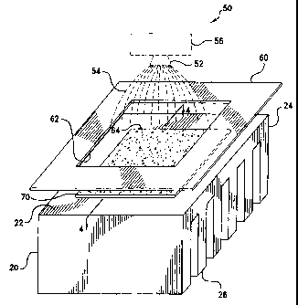
Referring next to Fig. 3, an illustrative spray application of the admixed PCM-
diluent
composition to a thermal dissipation member such as heat sink 20 of Fig. 1 is
described in
connection with the system shown at 50. System 50 includes a nozzle, 52, with
an orifice of a
select diameter, through which the composition is delivered onto the heat sink
heat transfer
surface 22 as the atomized or other spray stream referenced at 54. Nozzle 52
is provided to be in
fluid communication with a material supply, represented in phantom by block
56, which may be
part of an automated spray apparatus or, alternatively, an aerosol can.
For confining spray 54 to a select area of heat transfer surface 22, a
removable mask, 60,
optionally may be interposed between surface 22 and nozzle 52. Mask 60 is
provided as having
one or more apertures, one of which is referenced at 62, with margins
corresponding to the
desired outer periphery, referenced at 64, of interfacing 30 which is shown in
Fig. 3 as the
generally rectangular pad referenced at 70. Alternatively, the composition may
be sprayed from
nozzle 52 without the use of a mask 60 to cover substantially the entirety of
surface 22.
So deposited onto surface 22, the composition may be cured to hardened or
solidify into
a form stable, generally self-adherent film by drying, volatilizing, or
otherwise evaporating the
diluent. In this regard, depending upon the diluent, the coated heat sink may
be heated in an
oven, furnace, or the like to an elevated temperature of between about 70-125
C effecting the
volatilization of the diluent. Alternatively, the composition may be dried
under ambient
conditions or under conditions of reduced humidity to evaporate the diluent
leaving a residue film
of the PCM on surface 22. Film thicknesses of less than about 2 mil (0.05 mm)
may be achieved
using the spray application of the present invention.
Unlike greases or waxes, the cured pad 70 advantageously is form-stable at
normal room
temperature in a solid, semi-solid, crystalline, or glassy phase which is
converted at elevated
temperatures into a flowable liquid, semi-liquid, or otherwise viscous,
thixotropic phase. In its
form-stable phase, however, pad 70 and heat sink 20 may be shipped and handled
without
causing the PCM to slump, sag, or run, and thereby facilitates the attachment
of heat sink 20 to its
associated electronic component 12 (Fig. 1).
CA 02355171 2008-11-05
18
For further ease of use, and as may be seen with reference to Fig. 4, the
exposed surface
72 of PCM pad 70 may be coated with a thin layer 74, of a silicone, acrylic or
other pressure
sensitive adhesive to affix heat sink 20 to component 12 during installation.
As is common in the
adhesive arts, a release sheet,,76, may be provided as a strip of a waxed,
siliconized, or other
coated paper or plastic sheet or the like having a relatively low surface
energy so as to be
removable without appreciable lifting of pad 70 from surface 22.
Representative release sheets
include face stocks or other.films of plasticized polyvinyl chloride,
polyesters, cellulosics, metal
foils, composites, and the like.
With pad 70 so applied and with release sheet 76 protecting the adhesive layer
74
thereof, heat sink 20 may be packaged and shipped as an integrated unit to an
electronics
manufacturer, assembler, or other user. The user then simply may remove
release sheet 76 to
expose the adhesive layer 74, position such layer on heat transfer surface 18
of electronic
component 12 (Fig. 1), and lastly apply a clip or other another means of
external pressure to heat
sink 20 in thermal adjacency with component 12
The Example to follow, wherein all percentages and proportions are by weight
unless
otherwise expressly indicated, is illustrative of the practicing of the
invention herein involved, but
should not be construed in any limiting sense.
EXAMPLE
A phase change thermal interface was prepared in accordance with the present
invention
for characterization. A commercial boron nitride (BN)-filled, form-stable PCM
.(THERMFLOWTM 705, Parker Chomerics, Woburn, MA) was thinned with organic
solvents to
about 15% total solids by weight to yield a fluent, liquid solution. The
solution was sprayed
using a packaged spray can with a ball agitator onto the bottom surface of a
commercial 1.75 inch
(4.5 cm) by 1.75 inch (4.5 cm), pin fin heat sink (Wakefield Engineering,
Inc., Beverly, MA),
and then=dried to leave an adherent film residue having a thickness of about 2
mil (0.05 mm).
The heat sink so prepared was surface mounted using a clip under an
application pressure
of less than about 5 psi (35 kPa) to an Intel Pentium II 266 MHz
microprocessor chip.
CA 02355171 2001-06-13
WO 00/36893 PCT/US99/20750
19
Differential temperature measurements were obtained using thermocouples
attached to the chip
case and heat sink, with the ambient temperature within the computer also
being measured. At
steady-state, i.e., after about 40 minutes, final temperature measurements
were recorded.
The experimental results, wherein all temperatures are in C, are summarized
in Table 2
as compared to the performance of a similar assembly incorporating a
conventional dry film
thermal =interface material (THERMFLODJTm 705, Parker Chomerics) having a
thickness of
about 5 mil (0.125 mm).
Table 2
Comparative Thermal Performance of Experimental
Sprayed and Conventional Dry Film PCM Interfaces
Sample Thickness Tambient Tcase Tsink ATcase-sink
Sprayed 2 mil (0.05 mm) 35.0 54.15 53.72 0.43
Dry 5 mil (0.125 mm) 34.0 53.65 53.7 0.65
The foregoing results confirm that a sprayed, thin film phase change thermal
interface
offers improved performance as compared to a thicker, conventional dry film.
The interfaces of
the present invention accordingly may be employed in high density, high
frequency, or other
critical service applications with a high degree of confidence.
As it is anticipated that certain changes may be made in the present invention
without
departing from the precepts herein involved, it is intended that all matter
contained in the
foregoing description shall be interpreted as illustrative and not in a
limiting sense. All
references cited herein are expressly incorporated by reference.