Note: Descriptions are shown in the official language in which they were submitted.
CA 02355689 2001-06-15
WO 00/38448 PCT/EP99/10014
FLEXIBLE CDMA COMBINER
Field of the invention
The present invention relates to a combiner for combining
digital data samples from a predetermined number of inputs to
a predetermined number of outputs, for example from a
predetermined number of channels, onto a predetermined number
of carriers of a digital communication system.
In telecommunication systems, a large number of channels,
e.g. user channels containing voice or data signals, may be
transmitted together via the same transmission medium, for
example, via the same radio frequency band. A multitude of
access schemes for placing the data of the user channels on
the transmission medium is known. One class of transmission
schemes simultaneously transmits a plurality of different
user channels, e.g. in a radio frequency band, in such a way
that they overlap in, the time domain as well as in the
frequency domain. A well-known access scheme of this class is
the CDMA (Code Divie;ion Multiple Access) scheme.
Although the invention is not limited to the CDMA scheme and
may be used in any digital communication system where a
number of digital data samples from a predetermined number of
inputs (e. g. user criannels or some sort of preadded channels)
must be combined flexibly onto a predetermined number of
outputs, (e. g. carr~_ers), the invention in particular relates
to a flexible CDMA c:ombiner, where the digital data samples
are represented by weighted chips generated in a base station
of a CDMA radio communication system.
Background of the invention
Fig. 1 shows a typical block diagram of a conventional
baseband CDMA transmitter in a CDMA base transceiver station
CA 02355689 2001-06-15
WO 00/38448 2 PCT/EP99/100I4
BTS. Data on a plurality of user channels ch-l, ch-2,...ch-n
are input to a channel encoder 1. Apart from channel coding
itself, the channel encoder 1 may perform a QPSK modulation,
time-alignment of the user data etc. The channel encoder 1
outputs a possibly camplex-valued output data symbol stream
(ODSS) which is input. to a spreader/power weighting unit 2
which receives spreading codes and power weights for the
individual channels. Each user channel is spread with a
specific spreading code and after spreading each channel is
power weighted before all channels cpl, cp2, . . . cpn are output
to a combiner 3 where they axe combined. Note that cpl,
cp2,... cpn may refer to the real and imaginary parts of
complex-value channels. The output of the spreader/power
weighting unit 2 are sets of weighted chips which are output
at a chip rate CLK. That is, within each period t~-tl, tl-
t2,...tk_1-tk a single weighted chip of each channel is
output parallely. Each weighted chip contains a predetermined
number of bits, i.e. each digital data sample has a
predetermined bit width (hereinafter denoted as in bit) due
to power weighting.
In a CDMA communication system a (geographical) area is
divided into several regions which are called sectors. In
each sector, at least one and possibly more carriers are used
where each carrier represents a particular frequency band.
Within each sector the carrier can have a different number of
channels. In the following description, the term "sector-
carrier" represents basically a combination of a particular
sector with a particular carrier (frequency band). The task
of the combiner 3 is to combine the data of all the channels,
which must be transmitted in a specific sector and on a
specific carrier. Thus, the combiner 3 is essentially an
adder which adds up the discrete instantaneous values of all
channels belonging to a given sector-carrier. As is indicated
in Fig. 1 there may be m sector-carriers sc-1, sc-2,...sc-m.
CA 02355689 2001-06-15
WO 00/38448 3 PCT/EP99/10014
Typically, in a CDNI~~ transmitter, the number of channels to
be added for each such sector-carrier is fixed by the
hardware implementation. Since a separate (but identical)
combiner hardware i:~ used for each sector-carrier, this
results in an equal number of channels on each sector-carrier
of a base transceiver station BTS. On the other hand, in
contradiction to this fixed equal number of channels, the
network operator of a CDMA system faces in practice a
different load in each of the sector-carriers. Therefore, the
network operator would like to configure a variable number of
user channels for each sector-carrier. For example, a base
transceiver station BTS on a highway requires a higher number
of user channels in the sectors covering this highway,
whereas other sectors (for example covering a rural or
mountainous area) may only have to handle a few user
channels. Furthermore, the load in the individual sectors
might also change over time, e.g. during rush-hours, holiday
seasons or trade fairs.
Thus, having a fixed number of channels per sector-carrier
implies that the network operator has always to provide a
high number of user channels for all sector-carriers no
matter whether or not they are actually required in a
particular point in time.
Thus, it is desirable to provide the network operator with a
flexible combiner, which allows the network operator to
tailor the number of available channels per sector-carrier
according to the load conditions in the system. With the
flexible combiner the network operator could buy a standard
base transceiver station BTS having the capability to process
a certain total number of channels, and could adapt the base
transceiver station BTS to the actual distribution of
channels over the sectors and carriers without wasting
ressources. The flexible combiner could return benefits also
to the supplier with less cost for adapting his equipment to
the customer's needs.
CA-02355689 2001-06-15 __-..____.._ __ _. 'C ,
27-11-2000 cP 009910014
4
Prior art solutions
When the number of channels to be combined onto a specific
sector-carrier is fixed and does not change over time a
combines as shown in Fig. 2-1 and denoted with reference
numeral 3-1 can be used. In this combiner.3-1 the channels
~P1 ~ ~P2 ~ ~3 ~ ~P4 are invariably combined onto the sector-
carrier sc-1 and the channels cpn_3, ~Qn-2~ ~Pn-1~ ~Pn are
combined onto the sector-carrier sc-m. The channels are
respectively added in pairs in the adders ADD1, and stored in
intermediate flip-flops FF1 whereafter the respective outputs
are added by an adder ADD2 and the output of the adder ADD2
,.. is stored in a further intermediate flip-flop FF2. This type
of circuit must be provided for each of the m sector-
carriers. For the example in Fig. 2-1, where 4 channels per
sector-carrier are combined, n (total number of channels) is
equal to m*4 (m: number of sector-carriers). The combines 3-1
in Fig. 2-1 has the disadvantage that the channels are
invariably combined onto the sector-carriers and furthermore,
the combines 3-1 needs; quite an extensive hardware, since the
respective circuits need to be provided m-times.
Fig. 2-2 shows a combines 3-2 which allows to reduce the
hardware complexity. Such a combines is described .in EP 98
121 518.9 showing the preamble of claim 1 and filed by the
same applicant as the present application. Essentially, the
combines 3-2 in Fig. 2-2 comprises m adders ADDS, rn flip-
flops FF5 and m flip-flops FF&. The outputs of the flip-flops
FF5 are respectively coupled to the input of the adder ADD5
which also receives the output of a respective multiplexes
MUX which is also provided m-times. If in Fig. 2-2, similarly.
as in Fig . 2 -1, again ~4 channels ( such as cpl , cp2 , cp3 , c~4 or
~Pn-3 ~ ~n-2 ~ ~Pn-1 ~ ~Pn) ~~re to be combined onto each sector-
carrier, then the resp~=_ctive adder ADDS and the respective
multiplexes MUX have to be operated at four times the chip
rate CLK in order to add one weighted chip of each of the
respective four channe:Ls in a single chip period 1/CLK. The
AMENDED SHEET
,. "n,_,
c
CA 02355689 2001-06-15
27-11-2_000 EP 009910014
limiting factor in Fig. 2-2 is thus the maximum operating
frequency of the adder.
The combiner 3-2 of Fig. 2-2 provides more flexibility than
the combiner 3-1, since for combining e.g. 8 instead of 4
channels per sector-carrier, the adder ADD5 could operate-at
twice the rate (i.e. 8*CLK) and the MUX could be provided
with 8 instead of 4 inputs while in the combiner 3-1 a
further hierarchical adder-stage would be necessary. However,
the flexibility problem, i.e. that e.g. cpI can only be used
for the output sc-1, remains the same.
Fig. 2-3 shows a combiner 3-3 which increases the
flexibility. The circuit in Fig. 2-3 is a modification of the
circuit shown in Fig. 2-1. In Fig. 2-3 the combiner 3-3
comprises a number of multiplexers MUX at each input of the
respective adder ADDS. For each sector-carrier, for example
the sector-carrier sc-1, the adder ADDS and the flip-flop FF3
are provided n/2-times and the multiplexer MUX is provided n-
times. A control signal. sel is applied to the individual
multiplexers MUX in order to allow the adding of
predetermined ones of the n-channels onto a single sector-
carrier. If certain channels are not configured for one
sector-carrier, they are set to 0 by the signal sel applied
to the multiplexes. Whilst the circuit in Fig. 2-3 is far
__ more flexible than the one in Fig. 2-2, since the combines
3-3 allows to combine any input user channel onto any desired
sector-carrier, there :is an extensive hardware necessary in
order to realize the circuit.
GB 2 295 527 A relates to a rake combiner/despreader
apparatus. Real and imaginary data samples are input
parallely from shift register bit-wides into a set of
registers, respectively provided for the real and imaginary
data samples. At the output of each set of registers an
add/sub tree is provided commonly for all the registers. Two
switches respectively feed the added/subtracted data samples
,AMENDED SHEET
_._ __
CA 02355689 2001-06-15 --
27-11-x:000 EP 009910014
~a
into a accumulator means which is provided for carrying out a
matched filter operation. Thus, a set of n bits from n inputs
stored in n registers are combined onto m bit positions in
the respective accumulator.
Summary of the invention
As explained above, the disadvantage of the combiner 3-1 in
Fig. 2-1 is that it provides the same maximum number of e.g.
4 channels to a respective sector-carrier. Furthermore, each
channel is invariably attributed to a specific sector-
carrier. Therefore, it is for example not possible to feed
any of the channels cpn_3... cpn to a sector-carrier other than
~4MENDED SHEET
CA 02355689 2001-06-15
WO 00/38448 PCT/EP99/10014
6
sc-m. Thus, the circuit in Fig. 2-1 offers no flexibility and
the hardware is inefficiently used. The combiner 3-2 infFig.
2-2 uses the hardware more efficiently due to the provision
of the multiplexer IHUX, but it still has no flexibility
because it still provides the same number of e.g. 4 channels
to a predetermined sector-carrier and does not allow to feed
the channels to an arbitrarily selected sector-carrier.
Whilst the combiner 3-3 maximizes the flexibility and allows
to combine any channel onto any desired sector-carrier, the
hardware is very extensive to realize such a circuit. That
is, hardware is wasted, because some of the adders may not be
needed in particular ones of the sectors. If one considers
that a typical number for n in a CDMA radio communication
system is n = 24 (furthermore, in a practical implementation,
each of 24 input channels to the combiner could be
constituted by 32 px~eadded channels, i.e.
cpl=chl+ch2+...ch32; cp2=ch33+ch34+...ch64 etc.,where "ch"
denotes a particular- user channel), there is an extremely
high hardware effort. necessary to realize the flexibility in
channel combining when using the circuit 3-3 in Fig. 2-3.
The object of the present invention is to provide a combiner
which can combine in a flexible way a predetermined number of
user channels onto a. predetermined number of carriers without
using complicated hardware.
Solution of the object
This object is solved according to the invention by a
combiner for combining digital data samples from a
predetermined number n of inputs onto a predetermined number
m of outputs, said digital data samples having a
predetermined bit width and arriving parallely at said
combiner as data sets respectively consisting of one data
sample from each input at a predetermined common sample rate
CLK, including a plurality of k subprocessing units SU1,
SU2,...,SUi_1, SUi,...,SUk which each comprises
CA 02355689 2001-06-15
WO 00/38448 PCT/EP99/10014
7
an input register for downsampling and storing arriving data
sets at a clock rates of CLK/k; and a multiplex/add means for
receiving said data sets stored in said input register and
for outputting at said clock rate of CLK/k, for each of said
m outputs, an added data sample respectively formed by an
addition of predetermined ones of said stored data samples;
and a selector for cyclically selecting at said common data
rate CLK from said multiplex/add means of said subprocessing
units a respective output data set consisting of said m added
data samples; and wherein the sampling phase of the input
register of subprocEasing unit SUi is delayed by 1/CLK with
respect to the samp~.ing phase of the input register of the
subprocessing unit ~~Ui_1 with i in the range of 2,...,K .
Such a combiner provides for two kinds of flexibility, namely
each input channel can reach each output and the number of
input channels to beg combined onto an output can be variable
from output to output. The principle idea of the invention is
to provide a plurality of subprocessing units each of which
is provided with a respective set of data samples at each
k-th chip period, i.e. at a rate of CLK/k. In the
subprocessing units the selection and adding is carried out
at an oversampling rate which is higher than the chip rate.
The output of each scubprocessing unit is an intermediate
downsampled result for the outputs (sector-carriers) Z to m.
The selector reads out these intermediate results and
interleaves them to form a result at the chip rate CLK.
Therefore, instead of providing a large number of
multiplexers as in F'i.g. 2-3, the basic concept of the
invention is to provide subprocessing units k-times whilst
increasing the processing rate in the subprocessing units.
Therefore, the flexibility is maintained and the hardware
complexity is minimized. Thus, the hardware costs can be
reduced.
_ -.- _ - -- - _ __--
CA 02355689 2001-06-15
27-11-x'.000 cP 009910014
8
Advantageous embodinnents
Each adder in the subprocessing unit can preferably comprise
a first adder register taking in said samples selected by
said multiplexer at said clock rate of OS*CLK and an addition
unit receiving as inputs an output from said first adder
register and an output from an adder multiplexer and
outputting added samples of said inputs to a second adder
register taking in said added samples at said clock rate of
OS*CLK, said adder mu:Ltiplexer receiving as inputs an output
from said second adder register and a digital "0" signal,
w similarly as the adder shown in Fig. 2-2.
Further advantageous embodiments of the invention are listed
in the dependent claims. Hereinafter, the invention would be
described with reference to its advantageous embodiments.
However, it should be noted that the teaching as disclosed in
the description is not limited to the specially preferred
embodiment which is currently considered to be the best mode
of the invention.
Brief description of the drawings
_. Fig. 1 shows a principle block diagram of a baseband CDMA
transmitter;
Fig. 2-1 shows a firsts example of a CDMA combiner according
to the prior art;
Fig. 2-2 shows a second example of a CDMA combiner according
to the prior art;
,AMENDED SHEET
CA 02355689 2001-06-15
WO 00/38448 PCT/EP99/10014
9
Fig. 2-3 shows a third example of a CDMA combiner according
to the prior art;
Fig. 3 shows a principle overview diagram for explaining
the principle of the invention;
Fig. 4 shows an embodiment of the subprocessing unit Sk
shown in :fig. 3 together with the input means IM,
the output means OM and the selector M3; and
Fig. 5 shows the combiner of Fig. 3 where a more concrete
circuit configuration is shown for each of the
subproces:aing units S1, S2 together with a control
logic CL;
Fig. 6 shows a functional block diagram of a RAKE
receiver; and
Fig. 7 shows a functional block diagram of a RAKE receiver
using a combining technique according to the
invention.
It should be noted that in the drawings the same reference
numerals denote the same or similar parts throughout.
Hereinafter, the pr~~nciple of the invention will be described
with reference to F~_g. 3.
Principle of the invention
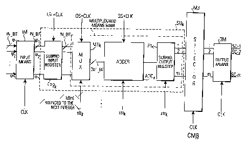
Fig. 3 shows a principle block diagram of a combiner CMB
operating according to the principles of the invention. It
should be noted that: Fig. 3 and the following figures refer
to a CDMA communication system, where the digital data
samples are respectively weighted chips output from a
spreader/power weighting unit ~ as shown in Fig. 1. However,
the invention can be: applied to any other application (e. g.
in a RAKE receiver) where digital data samples from a
plurality of inputs are to be combined onto a number of
outputs in a very flexible way.
CA 02355689 2001-06-15
WO 00/38448 PCT/EP99/10014
As shown in Fig. 3, digital data samples, such as weighted
chips (each set has a predetermined bit width as explained
below) arrive parallely at said combiner CMB. In Fig. 3 a
"set of weighted chips" denotes the samples arriving e.g.
between tp and tl. 'Thus, a set of weighted chips consists
exactly of n weight.=d chips, i.e. one chip per channel. As
explained with reference to Fig. 1, the data sets of weighted
chips arrive at a predetermined common sample rate (chip
rate) CLK. It should be understood that in the CDMA system
each weighted chip consists of a predetermined number of
bits. The sets of wfsighted chips are applied in a specific
manner to subproces;~ing units SU1, SU2...,SUk at the chip
rate. In total there. are k subprocessing units SU1, SU2...,
SUk and a selector M3 is provided for all subprocessing
units. As is indicated with the block "out" on the right side
of the selector M3, the output "out" from the combiner CMB
are m added (combined) weighted chips for m sector-carriers.
The output from the selector M3 also has a rate equal to the
chip rate.
Whilst in Fig. 3 each small squared box in the block "in" on
the left side corre:~ponds to one weighted chip of each
channel, the small :squared boxes in the block "out" on the
right side of the selector M3 correspond to added data
samples, i.e. a predetermined number of digital data samples,
i.e. a predetermined number of channels have been added up
for each sector-carrier at each output clock period 1/CLK.
Although the hatching used on the left side squared boxes and
on the right side squared boxes is the same, it should be
understood, that they boxes on the right side correspond to
added weighted chip: whereas the boxes on the left side
correspond to single weighted chips per channel.
As is indicated with the arrow on the right side of the
subprocessing unit E;U1, each subprocessing unit calculates
the combination of digital data samples for m sector-
carriers. That is, in contrast with the prior art combiners
CA 02355689 2001-06-15
WO 00/38448 PCT/EP99/10014
11
shown in Fig. 2-1, Fig. 2-2 and Fig. 2-3, in the inventive
combiner in Fig. 3 no hardware (or even parts of hardware) is
specifically dedicated to a particular sector-carrier.
However, there is a. hardware subprocessing unit which
calculates output values (added digital data samples) for all
sector-carriers. Since one such subprocessing unit cannot
produce all results at the chip rate, k subprocessing units
working on downsampled input sequences are used such that
more time is gained to calculate the results for all sector-
carriers within one subprocessing unit sequentially. After
having calculated all m results within one subprocessing unit
for a set of weighted chips, i.e. for a set of digital data
samples collected from predetermined user channels, the
selector M3 switches through all results corresponding to
this subprocessing unit and outputs a set of m values.
Exactly one chip period later the selector M3 reads out all
results from the next subprocessing unit, for example the
subprocessing unit SU2. As is shown in the block "out" on the
right side of the selector M3, the result is that in the chip
period tk-tk~.l the subprocessing unit SU1 outputs its
results, i.e. the added weighted chips for all m sector-
carriers. This is followed in the next chip period by the
output from the subprocessing unit SU2 and this is continued
until the subprocessing unit SUk outputs its results in the
clock period beginning with tzk-1. Exactly at the end of
reading out the data from the subprocessing unit SUk, it is
the subprocessing unit SU1 which has finished its selection
and adding process for the next set of weighted chips and
therefore in the chip period beginning with t2k again the
subprocessing unit SU1 is read out.
As explained before, the processing is therefore distributed
to k subprocessing units which however must operate at a
higher (i.e. oversampling) rate. Thus, no subprocessing unit
is dedicated to a specific channel. The subprocessing units
SU1, SU2... SUk are respectively provided for combining
respective weighted chips for all m sector-carriers and the
selector M3 performs a cyclic reading of the subprocessing
CA 02355689 2001-06-15
WO 00/38448
PCT/EP99/I0014
12
units. One can say that each subprocessing unit is dedicated
to combine channels at a rate k times inferior to the chip
rate and to produce outputs for all sector-carriers at this
reduced rate, i.e. SU1 for the chip periods tk-tk+1~ t2k-
t2k+1 etc., SU2 for the chip periods beginning with tk+1~
t2k+1 etc.
In order that the selector M3 can respectively access or read
out the respective subprocessing units SU1, SU2,...SUk in the
respective chip period, the subprocessing units must operate
at a higher speed such that in the worst case each
subprocessing unit is capable to produce per k/CLK period
(i.e. not per 1/CLK .period) m added weighted chips resulting
from an addition of weighted chips from all n channels.
Therefore, if n designates the number of channels, and k
designates the number of subprocessing units, then an
oversampling rate OS of OS=n/k must be used for the adding
process within each :~ubprocessing unit. This is indicated
with the rectangular blocks bll, b12~ b2~ b3 of the data sets
shown above each subprocessing unit. That is, the respective
set of weighted chip: must be held k chip periods, i.e. the
clock rate for inputting and holding new data in the
subprocessing unit i:~ CLK/k if CLK designates the chip rate
at the input. Since the selector M3 cyclically reads out data
from k subprocessing units, it :is clear that the
subprocessing units must finish their combining (adding) of
data values for n input chips and m sector-carriers within k
chip periods.
That is, since each subprocessing unit must add at most n
weighted chips at a rate of CLK/k (to calculate m results),
its adder must operate at n*CLK/k, i.e. at OS*CLK. That is,
not the number of results is decisive but the total number of
additions which are needed fox all results together.
For example, within the time period tQ-tk, the addition and
holding for all weighted chips of the blank squared boxes in
CA 02355689 2001-06-15
WO 00/38448 PCT/EP99/10014
13
the block bll is carried out. Only k chip periods later the
next set of chips (vertically hatched b12) need to be
processed in the subprocessing unit SU1, since the k-1 other
subprocessing units take care of the adding of chips in the
chip periods starting with tl...tk-1 (left... right hatched
squared boxes). This processing is taken over by the
subprocessing unit SU2 etc. up to the chip period tk_1 in
which the data is combined by a subprocessing unit SUk.
Therefore, the respective blocks bll, b12, b2, b3
respectively indicate that the input data is held for k
pulses of the clock CLK. It is also clear, that due to the
sequentially arriving data sets at periods tp, tl, t2...tk-1,
tk the start of a processing in subprocessing unit SUi is
delayed by exactly one chip period with respect to the
previous subprocess:ing unit SUi_x.
As indicated with the block bpipe, within the processing
units the results for each sector-carrier are generated
sequentially. That as, first the added weighted chip for the
first sector-carrier 1 is calculated wherein the adding is
performed sequentially for the required channels.
Subsequently, the added weighted chip for the second sector-
carrier is produced.. Since the processing for the second
sector-carrier can only start once the processing for the
first sector-carrier has been finalized, the processings per
sector-carrier are delayed as indicated in the block bpipe.
However, all m resu7_ts are ready when the next set of chips
arrives, such that t:he first subprocessing unit SU1 can again
start with a proces~~ing for the weighted chips beginning at
tk. Thus, the solution is based on a kind of delayed pipeline
processing together with the cyclical reading by the selector
M3. This procedure uses the processing capabilities very
efficiently and therefore reduces the hardware costs.
It should be noted that the order of processing for the
sector-carriers within each subprocessing unit is fully
CA 02355689 2001-06-15
WO 00/38448 PCT/EP99/10014
14
flexible. Only one restriction exists, namely that each
weighted chip can only be added to one sector-carrier output.
Furthermore, it should be noted, that the number of
subprocessing units k can be freely selected. Of course, at
each cycle of OS*CLK one channel can be processed depending
on the oversampling rate OS. For example, if the oversampling
rate is OS=8 and the number of channels is n=24, then
k=n/OS=3 subprocessing units will be used operating
internally at a processing speed of OS*CLK=8*CLK.
Therefore, one can say that an input means IM inputs the sets
of weighted chips (sets of digital data samples) at the chip
rate to all subprocf~ssing units SU1, SU2, SUk. After
downsampling by a factor of k, each subprocessing unit then
calculates sets of rn added weighted chips at the downsampled
rate using a processing clock of OS*CLK. The selector M3
reads out the sets of added weighted chips cyclically from
the subprocessing units at the common chip rate CLK. An
output means OM outputs the respective data sets.
As can be understood from the above description of the
combiner CMB in Fig. 3 according to the invention, there is
the flexibility that: each sector-carrier can be provided (at
chip rate) with added weighted chips resulting from arbitrary
combinations of input weighted chips of an arbitrary number
of channels, i.e. from all n channels if there is the
necessity to do so. On the other hand, only k subprocessing
units operating at t:he higher speed of OS*CLK are needed.
Thus, the hardware amount necessary is drastically reduced
while the flexibility to combine any channel with any other
channel onto arbitrary sector-carriers is fully provided.
Furthermore, the following advantages are achieved by the
combiner according to the invention:
1. The flexibility to allocate a variable number of
channels to each sector-carrier is achieved. This is
very much needed by the network operator to be able to
CA 02355689 2001-06-15
WO 00/38448 PCT/EP99/10014
~5
configure the number of available channels to fit the
expected traffic conditions (highway t~ mountains).
2. The flexibility to temporarily add more channels to a
sector-carrier is provided, something that is needed for
the operator to handle different traffic loads at
different times (e.g. holiday times, repair of a
neighboring base station, trade fares, ...) as explained
in the introduction.
3. The flexibility to provide any combination of an
arbitrary subset of channels to any given sector-carrier
such that the ~~hannels can be switched from another
sector-carrier at a given time due to the foreseen or
predicted traffic gradient.
4. The component reuse is very high resulting in very
little hardwarE~ costs. At least 85% of the hardware can
be saved in comparison with the solution in Fig. 2-3.
5. It is possible to generate a generic hardware for the
customer. That is, the hardware can be tailored by the
customer himse7_f/herself to his/her needs. This reduces
the costs for t:he manufacturer, since less variants and
less customizations in production will be necessary.
Hereinafter, a more specific block diagram of the combiner
CMB shown in Fig. 3 is illustrated and discussed in Fig.4,
whereas a specific circuit configuration of the subprocessing
units
SUk shown in Fig. 4 is illustrated in Fig. 5.
First embodiment of the invention
A combiner CMB shown in Fig. 4, combines digital data samples
from a predetermined number n of channels, e.g. user
channels, cpZ, cp2, . . . , cpn onto a predetermined number m of
_ -- _- ____-____ -__.___. -____ __ _ _____
CA 02355689 2001-06-15
27-11-2000 cP 009910014
16
outputs, e.g. sector-carriers sc-1, sc-2, ..., sc-m of a
digital radio communi<:ation system. It is also possible that
the channels are preadded channels. For example, in a
practical implementation, the n=24 input channels to the
combines could each be: constituted by 32 preadded channels,
i . a . cpl=chl+ch2+. . . ch?~2 ; cp2=ch33+ch34+. . . ch64 etc . , where
"ch" denoted a particular user channel.
The digital data samples have a predetermined bit width
in bit and arrive parallely at said combines as data sets
respectively consisting of n data samples at a predetermined
common data samples rate CLK. That is, at each fixed point in
time "tk" n data samples belonging to n channels arrive.
There are provided a plurality of k subprocessing units of
which the subprocessing unit SUk is shown in Fig. 4. An input
means IM inputs the data sets to each of said k subprocessing
units at said common data rate CLK.
As shown in Fig. 4, each of said subprocessing units SUk
comprises an input register R2k for storing the data sets at
a clock rate of CLK/k. A multiplexes Mlk is provided for
sequentially selecting a predetermined number of data samples
from a respective data set stored at said input register for
each of said m sector-carriers at a clock rate of OS*CLK,
where OS is an oversampling factor and k=n/OS. From a control
-- unit CL (shown in Fig. 5) the multiplexes Mlk receives a
select signal sltk which indicates the channels to be
combined.
An adder ADDk is proviaed for adding, fox each of said m
sector-carriers, said selected data samples into a respective.
added data sample (added weighted chip) at said clock rate
OS*CLK. An output register Flk is provided to store for said
m sector-carriers an output data set comprising said m added
data samples. The multiplexes Mlk, the adder ADDk and the
output register.Flk form, as shown in Fig. 4, a so-called
multiplex/add means MAM which is hereinafter also called the
data sample addition means.
I~MENDED SHEET -
CA 02355689 2001-06-15
WO 00/38448 PCT/EP99/10014
17
A selector M3, generally already described above with
reference to Fig. 3, cyclically selects at said common data
rate CLK from a respective output register of said
subprocessing units a respective output data set. An output
means OM outputs the selected data sets on said sector-
carriers SC-1,...SC-m at said common data rate CLK.
Although not shown in Fig. 4, of course the subprocessing
units SUk are provided k-times, whereas the input means IM,
the selector M3 and the output means OM are only provided
once, as will be further explained with reference to Fig. 5.
As is shown in Fig. 4, each respective data set consisting of
n data samples is held in the .input register R2k at the clock
rate of CLK/k. Since: the multiplexes MUX and in particular
the adder operate at the clock rate of OS*CLK (where OS =
n/k) it is possible to add for m sector-carriers sequentially
all input weighted chips. The timing within the subprocessing
unit is adjusted according to the worst case scenario, i.e.
for one sector-carrier the added weighted chip can consist of
an addition of all n input weighted chips from n channels
stored in the input register R2k. That is, the worst case
scenario is that all. cpl-cpn are added onto one sector carrier.
Therefore, all other sector-carriers give the value 0 (a
particular input channel cpi can then only go to one
determined sector-carrier scj and not to more than one).
If some added weighted chips only consist of an addition of a
smaller number of input weighted chips, then of course the
results can be stored in the intermediate output register Flk
earlier. However, this poses no problem, since the selector
M3 only accesses the. output register Flk at the rate CLK/k,
such that an earlier_ storage of values in the output register
is within the necessary reading timings of the selector M3.
Furthermore, as shown in Fig. 4, the adder ADDk must receive
a reset signal rstk from the control unit CL (shown in Fig.
CA 02355689 2001-06-15
WO 00/38448 18 PCT/EP99/10014
5) whenever the adding of the data samples has been finalized
for a given sector-carrier. That is, every k chip periods the
adder is reset at most m-times (if e.g. all m sector-
carriers are used, as in the above explained worst case
scenario). The output register Flk receives a storage signal
strk from the control logic CL when it is supposed to store
or read out a specific data set.
The input register R2k is necessary, since the data values
input from the input means IM must be kept available for a
period of time longer than the chip period. Otherwise, the
multiplexer MUX can not select flexibly all weighted chips
from all n channels to be added to one of the sector-
carriers. Whilst the multiplexer MUX performs a selection of
chip data, the adder ADDk performs a sequential adding of all
the chip data selected sequentially by the multiplexer MUX.
As explained above, the output register is necessary, since
the result (the added chip value or added digital data sample
value) may be available earlier for the case when not all n
chips are added and allocated to one sector-carrier.
Hereinafter, a more specific circuit configuration of the
block diagram of the inventive combiner CMB shown in Fig. 4
will be described with reference to Fig. 5.
Example of the subprocessing units
As explained with reference to Fig. 4 above, the input data
sets (sets of weighted chips in a CDMA system) arrive at the
combiner CMB at the chip rate CLK. Each digital data sample
(each weighted chip) is first stored in the input means IM
which is constituted by a register R1 in Fig. 5. As is shown
in Fig. 5, the storage takes place at the chip rate CLK. Each
digital data sample has a certain bit width in bit and the
input means R1 comprises a set of registers where the number
of the registers coz-responds to n, i.e. for n input channels
n words of a bit width in bit are to be stored (per channel
in'bit). There are n registers R1 because n input channels
CA 02355689 2001-06-15
WO 00/38448 PCT/EP99J10014
19
input respectively weighted chips or in general digital data
samples.
As explained above, the processing in the subprocessing unit
SU1, SU2,...SUk takes place with an oversampling factor OS
with respect to CLK Cfor example CLK = 4 MHz, OS = 8).
Therefore, the subprocessing unit is provided k = n/OS times.
Consider the example of n=24 and OS=8: at each cycle of
OS*CLK, one channel can be processed. To process all channels
within one subprocessing unit, 24 cycles of the rate OS*CLK
are needed. Since new sets of weighted chips arrive at the
rate CLK, these have to be stored at other subprocessing
units. At n/OS cycles of CLK, the results for all sector-
carriers are calculated within a substructure. Therefore, a
total number of k = 24/8 = 3 subprocessing units is needed to
process all channels; within one subprocessing unit.
Therefore, the contents of the register R1 changes at the
chip rate CLK. As explained above, within each subprocessing
unit SU1, SU2...SUk the respective weighted chips have to be
available longer than the chip period. Therefore, the input
registers R21, R22, R2k are provided with input values at the
rate CLK/k where it should be understood that also each of
the input registers R2 has a predetermined bit width in bit.
However, whenever a set of data values arrives, they are
parallely applied to each subprocessing unit SU1, SU2 as
shown in Fig. 5, thE: only difference being that the
subprocessing unit with the next higher index starts its
processing with a delay of a chip period 1/CLK. Thus, the
sampling phase of the input register R2i of subprocessing
unit SUi is delayed by 1/CLK with respect to the sampling
phase of the input register R2i_1 of the subprocessing unit
SUi-1. The registers R2, preferably realized as flip-flops,
have a rate of CLK/lc, wherein the subprocessing unit with the
next index is delayed by one clock cycle as is indicated in
Fig. 3. For example, if the same values as explained above
are used, then each register set R21, R22... has to have a
rate of CLK/3, since there are k=3 subprocessing units.
CA 02355689 2001-06-15
WO 00/38448 PCT/EP99/10014
The multiplexes M11 of the first subprocessing unit switches
the channels through. in the order, in which the channels
(more specifically their respective single weighted chips)
have to be added up for each sector-carrier sequentially. The
select signal sltk from the control unit CL indicates to the
respective multiplexes the indices of the channels to be
combined. That is, s~ltk does not indicate how many channels
are to be added, but which channel is to be switched through.
That is, the multipl.exer M11 (and also the other multiplexers
receives a select signal sltl from the control logic CL in
order to sequentially select data values from those values
stored in the input register R21. Of course, the multiplexes
also increases the bit width of the channels. Since the adder
must have a fixed bi.t width at its input and in the worst
case all channels are added to each other where the result is
transferred to one aector-carrier, the bit width may increase
to out bit =/(ld(n(~;in bit_1))\, wherein /x\ denotes the
ceiling operation selecting the smallest integer value equal
to or larger than x. If the value of a weighted chip,
represented in a twos-compliment, is negative, then the
multiplexes M11 prepends logic ones to the most significant
bits, otherwise zeros.
For example, when in~bit=3 and cp4 has the value -2, then the
twos complement of ~.> using 3 bits is 010. Inverting this
leads to 101 and adding 1 gives 110 H -2. When out bit=5 and
cp4 has the value -2,, then the twos complement of 2 using 5
bits is 00010, inverting this leads to 11101 and adding 1
gives 11110 t-~ -2. That is, for expanding the 3 bits which
are stored in regisi~er R21 (110) to 5 bits, the bit positions
4, 5 must be filled with ones. A negative value is always
recognizable at the most significant bit (here bit 3). If
this value is 1 (=negative) this means that the preceding
bits positions 4,5 are set to 1. If alternatively the most
CA 02355689 2001-06-15
WO 00/38448 PCT/EP99/10014
21
significant bit is 0 (=positive) the preceding bit positions
4, 5 are set to 0.
As is indicated in Fig. 5, the multiplexes M11 is connected
with the respective register which stores the respective
input weighted chip value from the respective channel cpl,...
cpn parallely and respectively outputs a single selected
weighted chip depending on the select signal sltl.
An adder ADDk, shown in Fig. 4, comprises a first adder
register R31, R32... taking in said samples selected by said
multiplexes at said clock rate of OS*CLK and an addition unit
SUM1, SUM2... receiving as inputs an input from said first
adder register and an output from an adder multiplexes MUX,
M21, M22... and outputting added samples of said inputs to a
second adder register R41, R42.., taking in said added
samples at said clock rate of OS*CLK, said adder multiplexes
receiving as inputs an output from said second adder register
R41, R42... and a digital "zero" signal. Furthermore, the
adder multiplexes ML:rX receives a reset signal rstk (rstl,
rst2,...) from the control logic CL. Essentially, the
combination of M11, R31, SUM1, R41 and M21 is according to
the combining apparatus disclosed in the above mentioned
European patent application EP 98 121 518.9 which is herein
incorporated in the present application via reference.
As is indicated in F'ig. 5, the registers R3 after the
respective multiplexes M1 have an oversampling rate of
OS*CLK. At each OS*CLK cycle another weighted chip of a
particular channel is stored, where the order of channel
indices will be fixed by the control logic by means of the
select signals sltk Csltl, slt2,...). The circuit after R3 is
basically an accumulator structure with the possibility to
switch the value 0 to the other input line of the adder. The
result of each sector-carrier is now calculated sequentially
within each subproce:ssing unit by adding the switched through
CA 02355689 2001-06-15
WO 00/38448 22 PCT/EP99/10014
' weighted chips. When a new result is being calculated for a
sector-carrier, a zero value is switched to the second input
line of the adder w~_th the help of M2. This means, that the
first channel, which has to be calculated for this sector-
carrier is added with 0. This is stored in R4 which is driven
by the same oversampling rate OS*CLK. Now, there is the
possibility to coup7_e back this result and add it with the
next channel (weight:ed chip) selected by the n-to-1
multiplexer M1. When a result is obtained for a sector-
carrier, the contro7_ logic gives an enable signal to one of
the flip-flops F1 which constitute the subprocessing output
register F11 shown in Fig. 4. Thereafter, the result for
another sector-carrier can be calculated with the accumulator
structure.
When all results are' calculated for every sector-carrier
within one subprocessing unit and these are stored in the
said flip-flops Fl, they are switched through by the
multiplexer M3 to tree set of registers R5 operated again at
the chip rate. The flip-flops F1 constitute the adder output
registers Flk shown in Fig. 5. The register R5 corresponds to
the output means OM shown in Fig. 4.
In parallel, as is indicated in Fig. 3, the next set of
weighted chips (data sets) is processed by the second
subprocessing unit SU2 in the same way (the subprocessing
unit SU2 does not wait until the subprocessing unit SU1 has
finished its operations and calculations). Therefore, the
control signals for this subprocessing unit are basically the
same. It is important to note that the processing in the next
subprocessing unit is delayed by one CLK cycle, since the
second set of weighted chips is stored one CLK cycle after
the first one and it: has to be processed in the same order
(it should be noted that order here means the sequence in
which the multiplexe:x M1 switches through the weighted
chips). For a sector-carrier, a continious stream of combined
output values is provided at the chip rate, wherein each
output value consists of a combination of one or more input
CA 02355689 2001-06-15
WO 00/38448 23 PCT/EP99/10014
samples arriving at 'the same time as is schematically
indicated in Fig. 3.
In all the above examples of flip-flops, it should be
understood that "f-lip-flop" designates an element, which is
clocked at a certain clock rate. An enable signal causes the
storage of the input of the flip-flop by the next active
clock edge.
That is, in Fig. 5 t:he data sets are respectively stored in
the input registers :R2 for a time period corresponding to the
clock rate of CLK/k. The multiplexer M1 performs a sequential
selection of chips (digital data samples) dependent on the
select signal sltk of the control unit CL. The adding
structure consisting of the register R3, the adder SUM, the
register R4 and the multiplexer M2 operates to add the
sequentially selected weighted chip values into a single
combined (added) weighted chip value which is then provided
to the respective sector-carrier, i.e. to the respective
flip-flop F11 provided for this specific sector-carrier.
Whenever the adding ;process is started for a given output,
the multiplexer M21, in response to the reset signal rstl,
switches through a "0" value which is then applied to the
respective adding unit SUM1.
The circuit of the combiner CMB in Fig. 5 allows the flexible
combination of channels in each subprocessing unit, since the
register R1 parallely applies the data set to the respective
input registers R21, R22 etc. The adding structure of the
register R3, SUM, R4 and the multiplexer M2 operate according
to known principles, namely sequentially to add up all chip
values for the relevant sector-carrier.
It should be stressed that the combiner according to the
invention can also be applied to complex-valued inputs. In
such an application, the combiner according to Figs. 3 to 5
may be realised twice (once for the real parts and once for
the imaginary parts of the inputs), wherein the control
CA 02355689 2001-06-15
WO 00/38448 2 4 PCT/EP99/10014
signals slt, rst and str are the same for the two combiners.
Alternatively, one may build a combiner with twice as many
inputs and twice as many outputs. Such an implementation is
described below with reference to Figs. 6 and 7.
Second embodiment of the invention
In addition to using the combiner according to the invention
in CDMA transmitters as explained with reference to Fig. 4,
S, the combiner can also be applied to CDMA receivers, in
particular to so-called RAKE receivers (see, e.g., K.D.
Kammeyer: "Nachricht:eniibertragung", B.G. Teubner, 2nd
edition, 1996, pp. E~58-672) .
Fig. 6 shows a funct=ional block diagram of a RAKE receiver.
Basically, it comprises a number L of so-called RAKE fingers
RF1, RF2, ..., RFL, a combiner RADD as well as a receiving
unit REC. In each RAKE finger the received complex baseband
signal RC sampled at: chip rate is multiplied with an
appropriately delaye=d channel-specific pseudo noise sequence
PN(dl), PN(d2),... F~N(dL) in the first multiplier ml, m2...mL
is added over the period of the PN sequence in the adder
SUM1, SUM2, SUML and is multiplied with an estimated channel
coefficient h *L-1, h *L-2,. h *p in the second multiplier
ml', m2'...mL', where the asterisk denotes complex
conjugation. Differe=nt delays dl, d2, ...dL are used for the
multiplication with the PN sequence in each RAKE finger. The
combiner RADD combines all outputs xl, x2 ...xL from the RAKE
fingers to the inputs Y of the receiving unit REC.
It should be underst=ood that Fig. 6 shows the functional
blocks necessary for the reception of a single channel. In
practice, many channels need to be received. In this case for
each channel a set of RAKE fingers as well as an additional
combiner are required. In Fig.7 the i-th RAKE finger for the
j-th channel is denoted RFij while the j-th addition node is
designated with RADDj, where i=1,..., L and j=1, ..., P. It
CA 02355689 2001-06-15
WO 00/38448 2 5 PCT/EP99/10014
is the task of each combiner R.ADD~ to combine (add)
predetermined ones of the RAKE finger outputs xl~, x2~, ...,
xL~ into a single output signal y~. Thus, considering all
adders R.ADD1, ...., RADDp together, the task of the overall
combiner RADD is to combine predetermined ones of the L*P
inputs onto a total of P outputs.
This task can be solved advantageously by the combiner
proposed in this invention. However, depending on the
modulation scheme used, the inputs and outputs of RADD may be
complex valued, so that the real and imaginary parts of the
inputs xi~ and outpuas y~ correspond to separate inputs and
outputs of the inventive combiner. Comparing the Figures 7
and 3-5, the following correspondences exist between the
respective inputs and outputs of the combiners and the
respective numbers c>f inputs an d outputs:
Re{x" ~ _ ~p, Re{yl ~ = scl 2LP = n
Im~x"~ _ ~pz Im{y,~=sc2 2P=m
Re{xz,~ _ ~p3 .
Im~xzz~ _ ~Pa ,
Re{yP} = sc(2P-1)
Im~yP } = sc2P
Re{xL,} _ ~PzL.I
Im{xL, ~ _ ~PzL .
Re { X LP ~ _ ~Q 2LP-I
Im{X LP} _ T zLP
CA 02355689 2001-06-15
WO 00/38448 2 6 PCT/EP99/10014
Thus, the inventive combiner explained above with reference
to Fig. 3-5 can be advantageously used for the combiner~RADD
of the RAKE receiver shown in Fig. 6, 7.
It should also be noted that, in this application, the
combiner according i~o the invention allows for a further
reduction in the hardware effort required. If the combiner
was realized as a separate hardware for each channel (c.f.
Fig. 2-1, 2-2), in <~ realistic application, it would have to
have a high number o.f inputs (e. g. L=8), because the number
of inputs would havfs to correspond to the number of Rake
fingers required in the worst case. For P=32 channels, a
total of LP=256 Rake finger processing units RFi~ would be
required in this example. On the other hand, when any Rake
finger output xi~ can be combined onto any receiving unit
RECD, as is the case with the combiner according to this
invention, the tota:L number LP of Rake finger processing
units can be calculated from the average number L of Rake
fingers necessary for each channel. For L=3, a total of 256-
LP=256-96=160 Rake :Finger processing units can be spared in
the above example while still providing the possibility to
allocate more than the average number L to some receiving
units.
Industrial applicability
The present invention can be used with any digital
communication system and not only with a CDMA communication
system using weighted chips for the combination of data from
the respective user channels. That is, the invention can be
applied to any apparatus where a need exists to add several
inputs in a flexible way in order to obtain added outputs. In
particular, without however being limited thereto, the
digital radio communication system is a CDMA radio
communication system, said digital data samples are weighted
chips output by a s;preading/power weighting unit of a CDMA
base transceiver station BTS of said CDMA system and said
CA 02355689 2001-06-15
cP 009910014
27-11-2000
27
outputs or carriers a=re sector-carriers respectively provided
for sectors of said CI~MA system.
Thus, the invention can be used in all digital communication
systems where a need :is generated that the digital data of a
plurality of user channels must be combined onto a
predetermined sector-carrier of a number of m sector-
carriers.
What has been describe=d above only refers to a particularly
preferred embodiment. That is, various modifications and
variations can be carried out within the invention as defined
with the appended cla~~ms.
Reference numerals in the claims only serve clarification
purposes and do not l~_mit the scope of protection of these
claims.
AMENDED SHEET