Note: Descriptions are shown in the official language in which they were submitted.
CA 02356323 2001-06-26
1
LASER DIODE DEVICE AND METHOD FOR THE MANUFACTURE
THEREOF
The invention is directed to a laser diode device according to the preamble
of patent claim 1. It is also directed to a method for the manufacture of such
a laser
diode device.
Such a device is known from the publication EG&G Optoelectronics:
Pulsed Laser Diodes -- PGEW Series, Internet Publication. A laser diode chip
achieves an output power of 15 watts and is built into a plastic housing. The
pulse
duration of the laser diode element amounts to 30 ns. The structure of the
laser diode
chip fundamentally corresponds to a multiple quantum well structure.
Such standard laser chips with a simple active zone, usually with quantum
well structure and in LOC (large optical cavity) technology as well, are
utilized for the
laser power range from 1 through 15 W and pulse durations of 5 through 100 ns
or
given pulse durations up to a few microseconds with lower powers. For cost
reasons,
the laser chip is built into a standard LED housing for a light-emitting
diode.
Subsequently, the chip is cast out, for example, with resin.
For required output powers above 15 W through about 50 W, said
publications provides for the mounting of a plurality of laser diode chips
next to one
another in the same housing. Such high output powers from laser diode in the
short
2 0 pulse range are required for a number of applications. Typical
applications are burglar
alarm systems and collision avoidance systems, LIDAR, optical range
measurement,
free space transmission, etc.
The above-described mufti-chip laser diode device is unfavorable for many
applications and, over and above this, is involved and, consequently,
expensive. First,
2 5 such a mounting of a plurality of chips in one LED housing is not standard
in the LED
production lines provided for the mass-production of LEDs and is difficult to
implement on these lines; second, the solution is expensive because of the
large chip
area that is required. For example, three laser diode elements are required
when the
CA 02356323 2001-06-26
2
output power is tripled. Finally, the externally effective radiation source
given the
chips arranged next to one another in the housing is distributed onto a
plurality of
emitters lying relatively far apart, which leads to deteriorated imaging
properties.
On the other hand, it is known to employ stacks of laser diode bars for
high laser output powers. The powers of the diode lasers are interconnected as
a
result thereof. In order to be able to control the thermal powers connected
therewith
given the higher optical output powers, the laser diode bars are often mounted
on
coolers and the components are utilized in combination. This is very involved
in
technical terms, and the focusability of the laser light deteriorates due to
the great
spacing of the individual radiation emitters as well as due to the larger
emitter area.
Due to the size of the mounted bars, difficulties derive in the combination of
a
plurality of radiation emitters above one another, as does, over and above
this, a
reduction of the beam quality. Such an arrangement of laser diode bars is
known from
a publication of DILAS Diodenlaser GmbH, Mainz-Hechtsheim.
The invention is based on the object of specifying a cost-beneficial laser
diode device with high power that is suited for manufacture on a large scale
and to
specify a method for the manufacture thereof.
This object is achieved by a laser diode device having the features of
patent claim l, by an employment according to claim 7 and by a method having
the
2 0 features of patent claim 8 or 9. Advantageous developments are the subj
ect matter of
the subclaims 2 through 6.
The present invention provides a laser diode device wherein a laser diode
chip is built into an LED housing, said laser diode chip being constructed as
a
multiple beam semiconductor laser diode that comprises a plurality of laser
stacks that
2 5 are arranged above one another on a semiconductor substrate and
respectively
comprise at least one active layer, whereby at least one pair of neighboring
laser
stacks has a tunnel junction arranged between them, and whereby the outer
surfaces of
the semiconductor substrate and of the uppermost laser stack respectively have
a
terminal contact that are connected to the terminals of the LED housing.
CA 02356323 2001-06-26
3
By employing monolithic laser diode stacks, on the one hand, extremely
high optical output powers up to 200 W or even more are possible in the short-
pulse
range; on the other hand, the chip area employed corresponds to that of a
single-laser
diode. Only a single chip need therefore be mounted in the housing. The chip
costs
of such a structure are considerably lower than the costs for a plurality of
chips having
the same total output power. As a result of the mounting of only a single
chip, the
laser diode device can ensue [sic] very beneficially on a standard production
line for
LED components. Over and above this, the light emitters of such a multiple
beam
laser diode lie close to one another, so that a focussing of the laser light
is easy to
1 o accomplish. Advantages in the unfocussed beam quality also derive.
It is provided that the multiple beam laser diode is of the type of an edge
emitter or of a surface emitter. The construction of such a multiple beam
laser diode
can have a single or multiple quantum well structure of a DFB structure.
The laser diode can be cast out with a transparent material, for example
resin or silicone, after the multiple beam laser diode has been built in.
Dependent on the type of LED housing, it is provided that the multiple
beam laser diode emits in one direction or in two directions. The output beam
or
beams of the multiple laser diode can be couple out of the housing either
directly or
via mirrors. As a result thereof, laser diode devices derive that can emit
toward the
2 0 top or toward the side given the mounting of the device on a motherboard.
LED
housings that are provided for surface mounting are especially advantageously
suited
here.
The invention is explained in greater detail below on the basis of the
Figures of the drawing. Shown are:
2 5 Figure 1 a schematic sectional view of a multiple beam high-performance
laser
diode installed in an LED housing for surface mounting;
Figure 2 a schematic, perspective view of a multiple beam high-performance
laser
diode for a radial LED housing;
CA 02356323 2001-06-26
4
Figure 3 a schematic, perspective view of a multiple beam high-performance
laser
diode in a radial housing;
Figure 4 the schematic layer structure of a multiple beam high-performance
laser
diode.
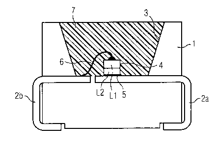
Figure 1 shows a crossection through an LED housing for surface
mounting (housing according to IEC Publ. 286 Part 3). The housing body 1 is
composed of high-temperature resistant thermoplastic with which an endlessly
punched conductor ribbon 2a and 2b is extrusion coated. At its inside, the
housing
has an opening whose sides 3 are fashioned as reflector surface. The
semiconductor
chip 4 with the structure of a multiple beam laser diode having two laser
stacks L1
and L2 in the exemplary embodiment between which a tunnel junction (not
referenced
in detail) is arranged has a first ohmic contact 5 applied on a terminal part
2a of the
housing in electrically conductive fashion. The electrical contact 5 is
applied on the
bottom surface of the semiconductor substrate of the multiple beam laser
diode. A
second ohmic contact 6 applied on the uppermost laser stack L1 is electrically
conductively connected to the other part of the terminal conductor ribbon 2b.
The semiconductor chip 4 containing the multiple beam laser diode can be
fashioned such that the two laser beams of the laser stacks Ll and L2 are
coupled out
via an edge of the active layers or via both edges. The individual beams are
deflected
2 0 with the assistance of the reflector surface 3 and are upwardly coupled
out of the
housing. The reflector opening is cast out with epoxy resin 7 for improving
the light
outfeed and for protecting the laser diode from environmental influences. The
resin 7
and the housing material are carefully matched to one another so that no
mechanical
disturbances can occur even given peak thermal loads. Some other transparent
2 5 material, for example acrylic resin, silicone or the like, can also be
utilized instead of
the casting resin 7.
A device according to Figure 1 with a multiple beam laser diode mounted
in an LED housing can be operated in the short-pulse range at up to 200 W and
above.
Since the chip area of the laser diodes stacked on top of one another
corresponds to
CA 02356323 2001-06-26
that of one single-laser diode and only one chip 4 need be mounted, the
mounting of
the semiconductor chip in the housing can ensue very cost-beneficially on a
standard
production line for LEDs.
The monolithic multiple beam laser diodes with laser stacks arranged on
5 top of one another, for example the stacks L1 and L2, are suitable for
pulsed operation
and contain at least two active laser zones that are connected to one another
with the
assistance of a junction. For example, the junction is a semiconductor tunnel
junction.
The laser stacks can have a single or multiple quantum well structure format
or some
other format. Typically, the layers are epitaxially deposited on top of one
another.
Standard vertical spacings between two neighboring light emitters amount to 2-
3 Vim.
During operation, the individual laser stacks arranged on top of one another
are
connected in series. Compared to single-laser diodes having the same output
power,
which is realized with different single-semiconductor [sic] chips, advantages
in view
of the focusability of the laser beams and in view of the beam quality also
derive
given the multiple beam laser diode.
Figure 2 shows a partially perspective view of a multiple beam laser diode
with the laser stacks L11 or, respectively, L21 that are mounted on a terminal
part 10
for a radial LED. The connection ensues via the ohmic terminal contact 15
under the
substrate. The other terminal contact of the multiple beam laser diode above
the
2 0 uppermost laser stack L11 has the terminal 16 connected to a second
outside terminal
11 of the device. The laser pulses P 1 and P2 that our emitted by the laser
stacks L 11
or, respectively, L21 are schematically indicated. Subsequently, the device of
Figure
2 is typically cast out with a transparent material.
Figure 3 shows an especially preferred exemplary embodiment wherein an
2 5 edge-emitting multiple beam high-performance laser diode chip 4 is mounted
on the
lateral surface of the terminal part 10 of a radial housing 9 known from light-
emitting
diode component technology, and the emission direction 8 proceeds parallel to
the
terminal legs of the radial housing 9. In this case, the edge-emitting high-
performance
CA 02356323 2001-06-26
6
laser diode chip 4 is first mounted on a lateral surface of the terminal part
and is
subsequently directly cast out with the radiation-transparent reaction resin
7.
By way of example, Figure 4 shows the structure of a multiple beam laser
diode as disclosed by US 5,212,706. The multiple beam laser diode contains the
laser
stacks L1 and L2 arranged above one another, between which a tunnel junction T
formed of the layers nT and pT lies. The lower laser stack L2 contains the
layers n2
and p2 that are separated by an active layer J2. The layer structure is
located above
the substrate n, which comprises an ohmic terminal contact 25 on its
underside. The
upper laser stack L1 comprises the diode layers pl and nl that are separated
by an
active layer Jl. Typically, the tunnel layers nT and pT are highly doped n-
layers or,
respectively, p-layers. A semiconductor layer p, on whose surface a second
ohmic
terminal contact 26 is located, is present above the upper laser stack L1.
Structure and function of the multiple beam laser diode are discussed in
detail in the aforementioned US Letters Patent. This is thereby a matter of a
GaAs
system. It is self evident that multiple beam laser diodes, too, can be
realized in other
material systems, for example in the InGaAs system. For example, such a
structure is
possible on the basis of two individual double quantum well structures (DQW)
that
are embedded in an LOC waveguide structure of AIGaAs and are connected to one
another via a tunnel junction placed in the gallium arsenide. The central
emission
2 0 wavelength of such an arrangement is dependent on the dimensioning of the
DQW
structure and preferably lies, for example, at 905 nm.
Multiple beam laser diodes as pulsed laser are possible in the entire
wavelength range from UV to above 1.5 pm covered by the III/V compound
semiconductors. In particular, the wavelength ranges around 850 nm and around
950
2 5 nm are of great technological interest. This particularly includes direct
applications in
the pulsed mode. The thermal load for the multiple beam laser diodes is low in
the
pulsed mode even given high optical output powers, so that the monolithically
stacked
laser diodes are not subject to any rapid degradation. This makes it possible
to use the
advantages of the high laser output powers with comparably good beam quality
in a
CA 02356323 2001-06-26
7
simple LED housing as well, without having to accept the disadvantages of
known
stack bars or of a high heat generation.
Dependent on the plurality of laser stacks lying above one another, the
output powers of the multiple beam laser diodes amount to approximately 70 W
given
two laser stacks lying above one another and 100 W given three laser stacks
lying
above one another. A 20-strip array chip processed in the above-described
material
system of InGaAs for the wavelength 905 nm has the dimensions 600 x 600 pmz
and
is mounted in a standard LED housing with reflector well and cast out (see
Figure 1).
The output power amounts to approximately 70 W, and the differential slope of
the
current/radiation characteristic is > 2.0 W/A. When three double quantum well
laser
structures are grown on top of one another in the same system, a multiple beam
laser
diode derives with an output power of about 100 W and a slop of the
characteristic of
> 3 W/A. It is possible to manufacture multiple beam laser diodes that have
even
higher output powers up to far more than 100 W.