Note: Descriptions are shown in the official language in which they were submitted.
CA 02356427 2001-06-26
WO 00/45505 PCT/US00/02393
BROADBAND AMPLIFICATION WITH HIGH LINEARITY
AND LOW POWER CONSUMPTION
Background of the Invention
This invention relates to apparatus and methods of broadband amplification
with
high linearity and low power consumption.
Broadband signal amplifiers and methods for amplifying signals over a wide
range of frequencies have many applications. For example, wireless
communication
devices, such as cellular telephones, cordless telephones, pagers, television
tuners, local
area networks, and the like, require wide dynamic range, high linearity
amplifiers to boost
the strength of received signals without distortion and cross-talk between
different
I S frequencies. Unfortunately, all linear amplifiers distort the signals they
are required to
amplify to some degree. This is particularly undesirable when two or more
independent
channels are being amplified. Under these circumstances, the amplifier
generates
unwanted intermodulation products that may cause interference and result in
poor
performance of the communication device.
Intermodulation distortion is defined in terms of the peak spurious level
generated
by two or more tones injected into a receiver. A receiver may be characterized
by a third-
order distortion figure of merit referred to as a "third-order input intercept
point" (IIP3),
which is defined as the input power (in the form of two tones) required to
create third-
order distortion products equal to the input two tone power. The linearity of
an amplifier,
and thus the immunity of the receiver to distortion and cross-talk, improves
with the IIP3
of the amplifier. Another amplifier figure of merit is equal to the ratio of
the maximum
microwave output power (at a specified level of distortion) to the applied DC
power.
The conventional method of specifying the level of distortion for this figure
of merit is
called the output intercept point of third order products (OIP3). In
accordance with the
OIP3 method, two input signals separated only slightly in frequency, and of
substantially equal, but adjustable, power are applied to the amplifier input.
A plot is
made of both the fundamental frequency output power and the power in the third
order
intermodulation product versus the input power and a linear extrapolation is
made of
these two plots. The point where these two extrapolations intersect is the
OIP3
CA 02356427 2001-06-26
WO 00/45505 PCT/US00/02393
amplitude, which is read in dB from the output power (ordinate) axis.
Amplifier linearity may be improved by increasing amplifier gain (see, e.g.,
Wheatley, U.S. Patent No. 5,732,341 ). This approach, however, increases the
power
consumption of the amplifier and, thereby, decreases the length of time a user
may
operate battery-powered receivers incorporating such amplifiers before the
batteries must
be recharged.
Summary of the Invention
In one aspect, the invention features an apparatus configured to amplify a
signal,
comprising: an input transistor and an output transistor coupled together in a
cascode
configuration with the input transistor defining an input of the apparatus and
the output
transistor defining an output of the apparatus; and a feedback network coupled
between
the input and the output and characterized by an impedance of substantially
zero
resistance and non-zero reactance.
Embodiments may include one or more of the following features.
The feedback network preferably has a reactance selected to reduce third-order
intermodulation distortion produced at the output of the apparatus. The
feedback network
preferably comprises a feedback capacitor. The feedback network preferably
consists
essentially of capacitive reactance.
In a preferred embodiment, an inductive feedback network is coupled between
the
input transistor and a low voltage reference and consists essentially of
inductive
reactance. An inductor preferably is coupled between the input transistor and
the low
voltage reference. The inductive feedback network and the capacitive feedback
network
may have respective reactances selected to achieve a desired impedance at the
input of
the apparatus.
The reactance of the capacitive feedback network is selected to achieve an
impedance at the input of the apparatus that is substantially independent of
frequency
over a broad frequency range. In one embodiment, the apparatus is configured
to amplify
a signal having a frequency of at least about 500 MHZ with substantial
linearity.
In some embodiments, a receiver input, configured to receive a wireless
signal, is
coupled to the apparatus input, and a receiver output, configured to produce
an output
signal representative of the wireless signal received at the receiver input,
is coupled to the
apparatus output.
In another aspect, the invention features a method of making an apparatus
2
CA 02356427 2001-06-26
WO 00/45505 PCT/US00/02393
configured to amplify a signal, comprising: forming on a substrate an input
transistor and
an output transistor coupled together in a cascode configuration with the
input transistor
defining an input of the apparatus and the output transistor defining an
output of the
apparatus; and providing a feedback network coupled between the input and the
output
and characterized by an impedance of substantially zero resistance and non-
zero
reactance.
In yet another aspect, the invention features a method of amplifying a signal
comprising: receiving an input signal at an input; amplifying the input signal
to provide
an output signal at an output; and sampling the output signal at the input
through a
feedback network characterized by an impedance of substantially zero
resistance and
non-zero reactance.
The output signal may be sampled at the input by coupling the output to the
input
through a feedback network that consists essentially of capacitive reactance.
The method
may further include the step of matching an output impedance by providing a
series
I S feedback network that consists essentially of inductive reactance.
In another aspect, the invention features an apparatus configured to amplify a
signal, comprising: first and second amplification stages, each comprising an
input
transistor and an output transistor coupled together in a cascode
configuration with the
input transistor defining an input of the amplification stage and the output
transistor
defining an output of the amplification stage, a capacitive feedback network
coupled
between the input and the output and consisting essentially of capacitive
reactance, and
an inductive feedback network coupled between the input transistor and a low
voltage
reference and consisting essentially of inductive reactance; wherein the
inputs of the
amplification stages are coupled together to form an input of the apparatus,
and the
outputs of the amplification stages are coupled together by an isolator.
In one embodiment, the isolator comprises a diode.
Among the advantages of the invention are the following.
The invention reduces (or rejects) the intermodulation products inherently
present
in non-linear amplifier circuits. The OIP3 is improved by at least 3-6 dB at a
given
supply current; or, the same OIP3 may be obtained at a lower power dissipation
(e.g., in
one embodiment, a 50% current reduction may be achieved). The low power
requirements of the invention makes it particularly useful for wireless
applications. The
inventive amplifiers and amplification methods described herein also achieve
an input
3
CA 02356427 2001-06-26
WO 00/45505 PCTNS00/02393
impedance and transfer characteristic that is flat over a broad frequency
range (at least an
octave). Furthermore, the IIP3 is easily adjusted, without changing other
circuit
parameters or specifications, by simply altering the supply current. Moreover,
matching
to a real input impedance is accomplished relatively easily. The invention is
also
substantially insensitive to fabrication process variations. The invention is
applicable to a
wide variety of applications, including various wireless circuits, without
sacrificing
important design parameters.
Other features and advantages will become apparent from the following
description, including the drawings and the claims.
Brief Description of the Drawines
Fig. 1 is a block diagram of a wireless receiver receiving a signal from a
transmitter.
Fig. 2 is a circuit diagram of a low power, broadband amplifier with shunt and
series reactive feedback networks.
Fig. 3 is a circuit diagram of a low power, broadband amplifier with a
capacitive
shunt feedback network and an inductive series feedback network implemented
with
bipolar transistors.
Fig. 4A is a circuit diagram of a low power, broadband amplifier with a
capacitive
shunt feedback network and an inductive series feedback network implemented
with field
effect transistors (FETs).
Fig. 4B is a circuit diagram of a low power, broadband amplifier with a
capacitive
shunt feedback network and an inductive series feedback network implemented
with a
FET and a bipolar transistor manufactured using a BICMOS process.
Fig. 5 is a circuit diagram of a switched gain amplifier formed from two low
power, broadband amplifier stages each having a capacitive shunt feedback
network and
an inductive series feedback network.
Description of the Preferred Embodiments
Referring to Fig. l, an apparatus 6 configured to amplify a signal (e.g., a
portable
wireless receiver, such as a cellular telephone) includes a receiver input 8,
an amplifier
10, a receiver output 12, and a power source 14 (e.g., a battery). Receiver
input 8 is
configured to receive an electromagnetic signal 16 (e.g., a signal with a
frequency that is
greater than 100 MHZ, and may be greater than S00 MHZ) from a transmitter 18
and to
produce an electrical signal 20. Amplifier 10 receives signal 20 and delivers
an amplified
4
CA 02356427 2001-06-26
WO 00/45505 PCT/US00/02393
signal 22 to receiver output 12, which converts amplified signal 22 into a
suitable output
signal 24 (e.g., sound representative of a human voice).
Although only a single electromagnetic signal I6 is shown in Fig. 1, other
signals
(at different frequencies) are typically received by receiver input 8. As
explained above,
S when two or more tones are received by receiver input 8, amplified signal 22
will contain
intermodulation products that may interfere with the desired input signal. The
intermodulation products which have the greatest adverse impact on the quality
of
amplified signal 22 are those which correspond to a third-order component of
the
intermodulation distortion represented by IM3, which includes 2f, - f and f, -
2 f
frequency components where f, and f are the frequencies of two tones
simultaneously
injected into wireless receiver 6. As explained below, amplifier I O is
configured to
reduce IM3 intermodulation distortion and, thereby, provide an improved
intermodulation
characteristic, without sacrificing the noise factor (NF) of the amplifier and
while
enabling the amplifier input to be impedance-matched with receiver input 8
with relative
ease. In the drawings described below, receiver input 8 is represented by a
voltage source
V;" and an output impedance Zo, and receiver output 12 is represented~by a
capacitor Co
and a load impedance Ro. Other configurations are possible.
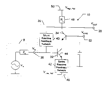
As shown in Fig. 2, amplifier 10 includes an amplification stage 30 that is
formed
from an input bipolar transistor 32 (e.g., a heterojunction bipolar
transistor) and an output
bipolar transistor 34 (e.g., a heterojunction bipolar transistor) coupled
together in a
cascode configuration with input transistor 32 defining an input 36 of
amplifier 10 and
output transistor 34 defining an output 38 of amplifier 10. A shunt reactive
feedback
network 40, which is characterized by an impedance of substantially zero
resistance and
non-zero reactance, is coupled between input 36 and output 38. Shunt feedback
network
40 has a reactance selected to reduce the IM3 intermodulation distortion
produced at
output 38 of amplifier 10. A series reactive feedback network 42, which is
characterized
by an impedance of substantially zero resistance and non-zero reactance, is
coupled
between the emitter 44 of input transistor 32 and a low voltage reference 46.
Series
feedback network 42 improves the linearity of amplifier 10 and, together with
shunt
feedback network 40, defines the input impedance of amplifier 10. The
reactances of
shunt feedback network 40 and series feedback network 42 are selected to
achieve an
input impedance of amplifier 10 that matches the output impedance (Zo) of
receiver input
8. Because only reactive components are used in shunt feedback network 40 and
series
5
CA 02356427 2001-06-26
WO 00/45505 PCT/US00/02393
feedback network 42, the noise factor (NF) of amplification stage 30 may be
optimized
by conventional design techniques. A bias impedance 48 couples the collector
of output
transistor 34 to a high voltage reference 50 to provide DC bias to
amplification stage 30.
A biasing network (represented by VB;~ biases the base 52 of output transistor
34.
Referring to Fig. 3, in one embodiment, shunt feedback network 40 consists of
a
feedback capacitor CF with a capacitance selected to reduce the IM3
intermodulation
distortion produced at output 38 of amplifier 10. Series feedback network 42
consists of
an inductor LSE with an inductance selected to improve the linearity of
amplification stage
30. By using excessive inductive series feedback (e.g., LSE with a value of
about 1-3 nH
for an operating frequency of about 2 GHz), series feedback network 42 is
linearized
without altering the NF. The values of CF and LSE are also selected to match
the output
impedance of receiver 8 (e.g., Zo has a value of about 50 ohms). In operation,
the shunt
capacitive feedback CF reduces the real part of the input impedance and also
offsets the
negative imaginary part of the input impedance (in some cases offsetting the
negative
imaginary part of the input impedance completely). This enables the input
impedance to
be matched easily with the output impedance of receiver input 8. In
addition,~shunt
feedback capacitor CF reduces (or rejects) the IM3 products because of the
favorable
phase of the IM3 products at amplifier output 38 with respect to amplifier
input 3b and
the fact that the AC current through CF is approximately equal to Vo,~.T
jc~CF. Bias
impedance 48 consists of an inductor Lcc.
The power gain (S2,) of amplification stage 30 may be approximated by:
RL
uuCF.RL +
_ wLSE _Zo
1 + Jc.~CF.RL RL
This approximation has been confirmed by simulation.
In an embodiment that is optimized for operation at frequency of about 2 GHz,
CF
has a value of about 140 fF, LSE has a value of about 1.5 nH, bias impedance
48 (RL) has
an impedance of about 200 ohms, Co has a value of about 1 pF, Lcc has a value
of about 7
nH, and Zo has a value of about 50 ohms. These parameter values result in an
amplifier
gain of about 14.3 dB L 70 ° independent of the supply current or
process used.
The embodiment of Fig. 3 may be manufactured using conventional
6
CA 02356427 2001-06-26
WO 00/45505 PCT/US00/02393
semiconductor device fabrication techniques. For example, the entire amplifier
circuit,
including amplification stage 30, bias impedance 48, and biasing network
(VB;~) may be
fabrication on a semiconductor substrate using conventional semiconductor
deposition
and ion implantation techniques, as well as conventional photolithography
patterning
techniques. Bipolar transistors 32, 34 may be formed using known bipolar and
heterojunction bipolar technologies.
Other embodiments are within the scope of the claims.
For example, referring to Fig. 4A, in another embodiment, amplification stage
30
is formed from an input field effect transistor (FET) 60 and an output FET 62
coupled
together in a cascode configuration. The other design components and the
operation of
this embodiment are similar to the corresponding components and operation of
the
embodiment described in connection with Fig. 3.
As shown in Fig. 4B, in yet another embodiment, amplification stage 30 may be
formed from an input bipolar transistor 70 and an output FET 72 coupled
together in a
cascode configuration and fabricated using a BICMOS process. The other design
components and the operation of this embodiment are similar to the
corresponding
components and operation of the embodiment described in connection with Fig.
3.
As shown in Fig. 5, a switched gain amplifier 80 may be formed from two
amplification stages 82, 84 coupled together in parallel. Amplification stage
82 includes
an input transistor 86 and an output transistor 88 coupled together in a
cascode
configuration, a shunt feedback capacitor 90, and a series feedback inductor
92.
Amplification stage 84 includes an input transistor 94 and an output
transistor 96 coupled
together in a cascode configuration, a shunt feedback capacitor 98, and a
series feedback
inductor 100. The bases of input transistors 86, 94 are coupled together to
form an input
102 of switched gain amplifier 80. The output of amplification stage 82 forms
an output
104 of switched gain amplifier 80. The output of amplification stage 84 is
coupled to
output 104 through a diode 106, which isolates shunt feedback capacitor 98
when
amplification stage 82 is turned on. Other techniques may be used to isolate
shunt
feedback capacitor 98. For example, diode 106 may be replaced by a CMOS
switch;
alternatively, diode 106 and feedback capacitors 90, 98 may be replaced by a
varactor
diode.
In operation, the gain of amplifier 80 may be changed by switching between
amplification stage 82 and amplification stage 84. When amplification stage 82
is turned
7
CA 02356427 2001-06-26
WO 00/45505 PCT/US00/02393
on, the input impedance is determined by shunt feedback capacitor 90 and
series feedback
inductor 92. When amplification stage 84 is turned on, the input impedance is
determined by shunt feedback capacitor 90, shunt feedback capacitor 98, and
series
feedback inductor 100. Thus, by proper selection of the shunt feedback
capacitors and
the series feedback inductors, the input impedance of amplifier 80 may remain
substantially constant. As in the embodiments described above, shunt feedback
capacitors 90, 98 have capacitances selected to reduce IM3 intermodulation
distortion
produced at output 104 of amplifier 80.
Still other embodiments are within the scope of the claims.
8