Note: Descriptions are shown in the official language in which they were submitted.
CA 02356938 2001-06-26
1
D E S C R I P T I 0 N
SEMICONDUCTOR DEVICE AND METHOD OF
MANUFAfTURING THE SAME
Technical Field
The present invention relates to a semiconductor
device and a method of manufacturing the same. More
particularly, the invention relates to a semiconductor
device that is sealed in resin in the form of a silicon
wafer and a method of manufacturing the same.
Background Art
A method of manufacturing semiconductor devices
called CSPs (Chip Size Packages) will be described with
reference to FIG. 17 to FIG. 20. First, as shown in
FIG. 17, connection pads 2 are formed on the upper
surface of a silicon wafer (semiconductor wafer) 1.
An insulating film 3 is then formed, covering the
i
upper surface of the wafer 1 and the connection pads 2,
except the center part of each connection pad 2.
Wirings 5 are formed, each on a limited region of
the insulating film 3 and on the center part of the
connection pad 2, which is exposed through an opening
4 made in the insulating film 3. Pillar-shaped
electrodes or column electrodes 6 are formed, each on
one end of the wiring 5. Regions 7 shown in FIG. 17
correspond to dicing streets.
Next, as shown in FIG. 18, a seal film 8 made of
CA 02356938 2001-06-26
2
epoxy-based resin or the like is formed on the upper
surface of the resultant structure including the
pillar-shaped electrodes 6. The seal film 8 is
a little thicker than the pillar-shaped electrodes 6
are tall. The seal film 8 therefore covers the pillar-
shaped electrodes 6. Then, the seal film 8 is polished
at its upper surface until the tops of the pillar-
shaped electrodes 6 are exposed as is shown in FIG. 19.
Further, the silicon wafer 1 is cut along the dicing
streets 7. Chips, or semiconductor devices 9, are
thereby manufactured as is illustrated in FIG. 20.
The semicondluctor devices 9 have been made by
cutting the silicon wafer 1 that has the seal film 8
formed on it along the dicing streets 7. The four
sides of each semiconductor device 9 are therefore
exposed. At the exposed sides, water or moisture may
enter the interface between the insulating film 3
1
(protective film) and the seal film 8, and may oxidize
the wirings 5 and. the like. Moreover, a crack or
cracks may develop in the interface between the
insulation film 3 and the seal film 8.
Disclosure of Invention
An object of the present invention is to provide a
semiconductor device that is resin-sealed at the sides,
too, which are exposed when the device is cut from
a wafer.
According to an aspect of the invention there is
CA 02356938 2001-06-26
3
provided a semiconductor device which comprises a
semiconductor substrate and a seal film. The substrate
has an upper surface, a lower surface opposing the
upper surface, sides extending between the upper and
lower surfaces, and a plurality of outer connection
terminals formed on the upper surface. The seal film
covers the upper surface of the semiconductor
substrate, exposes each of the outer connection
terminals at one surface, and covers the sides to at
least half the thickness of the semiconductor
substrate.
According to another aspect of invention there is
provided a method of manufacturing a semiconductor
device. The method comprises the steps of: preparing
a semiconductor wafer having an upper surface, a lower
surface opposing the upper surface, sides extending
between the upper and lower surfaces, and a plurality
I
of outer connection terminals formed on the upper
surface; making trenches in those parts of the semicon-
ductor wafer which lie between chip-forming regions
thereof, each trench reaching at least half the
thickness of the semiconductor wafer, and forming
a seal film on the upper surface of the semiconductor
wafer, filling the trenches and exposing the outer
connection terminals at one surface; and cutting the
seal film along the trenches, removing those parts of
the seal film which have a smaller width than the
CA 02356938 2001-06-26
trenches.
Brief Description of Drawings
FIG. 1 is a magnified, sectional view of a silicon
wafer having pillar-shaped electrodes on it, for
explaining a step of a method of manufacturing a
semiconductor device according to the first embodiment
of the invention;
FIG. 2 is also a magnified, sectional view of the
silicon wafer, explaining the step that follows the
step shown in FIG. l;
FIG. 3 is a magnified, sectional view of the
silicon wafer, explaining the step that follows the
step shown in FIG. 2;
FIG. 4 is magnified, sectional view of the silicon
wafer, explaining the step that follows the step shown
in FIG. 3;
FIG. 5 is magnified, sectional view of the silicon
wafer, explaining the step that follows the step shown
in FIG. 4;
FIG. 6 is magnified, sectional view of the silicon
wafer, explaining the step that follows the step shown
in FIG. 5;
FIG. 7 is magnified, sectional view of the silicon
wafer, explaining the step that follows the step shown
in FIG. 6;
FIG. 8 is magnified, sectional view of the silicon
wafer, explaining' the step that follows the step shown
CA 02356938 2001-06-26
S
in FIG. 7;
FIG. 9 is magnified, sectional view of the silicon
wafer, explaining the step that follows the step shown
in FIG. 8;
FIG. 10 is magnified, sectional view of the
silicon wafer, explaining the step that follows the
step shown in FIG. 9;
FIG. 11 is a magnified, sectional view of
a silicon wafer, ~=_xplaining a step of a method of
manufacturing a s~=miconductor device that is the second
embodiment of this invention;
FIG. 12 is a magnified, sectional view of the
silicon wafer, explaining the step that follows the
step shown in FIG. 11;
FIG. 13 is a magnified, sectional view of
a silicon wafer, explaining a step of a method of
manufacturing a semiconductor device that is the third
embodiment of this invention;
FIG. 14 is a magnified, sectional view of
a silicon wafer, explaining a step of a method of
manufacturing a semiconductor device that is the fourth
embodiment of the invention;
FIG. 15 is a magnified, sectional view of the
silicon wafer, explaining the step that follows the
step explained in FIG. 14;
FIG. 16 is a. magnified, sectional view of
a silicon wafer, explaining a step of a method of
CA 02356938 2001-06-26
6
manufacturing a semiconductor device that is the fifth
embodiment of the invention;
FIG. 17 is a magnified, sectional view of
a silicon wafer, explaining a conventional method of
manufacturing a semiconductor device;
FIG. 18 is a magnified, sectional view of the
silicon wafer, explaining the step that follows the
l step shown in FIG. 17;
FIG. 19 is a magnified, sectional view of the
silicon wafer, explaining the step that follows the
step shown in FIG. 18; and
FIG. 20 is a magnified, sectional view of the
silicon wafer, explaining the step that follows the
step shown in FIG. 19.
Best Mode for Carrying Out the Invention
FIGS. 1 to 7.0 show the steps of manufacturing a
semiconductor device according to the first embodiment
of the present irwention, with reference to the
figures, the structure of the semiconductor device will
be described, along with the method of manufacturing
the semiconductor device. First, an unfinished product
is prepared. As shown in FIG. 1, the unfinished
product comprises. a silicon wafer (semiconductor wafer)
1 and pillar-shaped electrodes (outer connection
terminals) 6 formed on the upper surface thereof.
Integrated circuits are provided in the inner area on
the silicon wafer 1. More specifically, the unfinished
CA 02356938 2001-06-26
7
product is prepared as follows. First, connection pads
2 are formed on tale upper surface of the silicon wafer
1 and are connected to the integrated circuits provided
on the silicon wafer 1. An insulating film 3 is then
formed, covering the upper surface of the wafer 1 and
the connection pads 2, except the center part of each
connection pad 2. The insulating film 3 is formed of
a single layer made of silicon oxide, silicon nitride,
or the like. Alternatively, the film 3 may be a multi-
layer film comprising a silicon oxide film, a silicon
nitride film or t:he like and an organic protective film
made of polyimide or the like. Wirings 5 are then
formed, each on a limited region of the insulating film
3 and on the center part of the connection pad 2, which
is exposed through an opening 4 made in the insulating
film 3. Finally, pillar-shaped electrodes 6 (outer
connection terminals) are formed, each on one end of
the wiring 5. Regions 7 shown in FIG. 1 correspond to
dicing streets in a shape of matrix.
Next, as shown in FIG. 2, a dicing tape 11 is
adhered to the lower surface of the silicon wafer 1.
The dicing tape :~1 is firmly adhered to the silicon
wafer 1 because its upper surface is coated with
adhesive. As shown in FzG. 3, the silicon wafer 1 is
cut along the dicing streets 7. In order to cut the
wafer 1 complete~~y, through its thickness, the dicing
tape 11 is cut, t:oo, in part or to half its thickness.
CA 02356938 2001-06-26
The silicon wafer 1 is thereby cut into semiconductor
substrates 1', each being a semiconductor chip.
Nonetheless, the substrates 1' will be collectively
called "silicon wafer 1," since the dicing tape 11
is adhered to the lower surfaces of the substrates 1',
fastening the semiconductor substrates 1' together.
Once the silicon wafer 1 is completely cut and the
dicing tape 11 is cut in part, trenches 12 having a
prescribed width are formed among the semiconductor
substrates 1'.
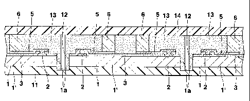
Thereafter, as shown in FIG. 4, a seal film 13
made of epoxy-based resin or the like is formed on the
upper surface of the silicon wafer 1 having the pillar-
shaped electrodes 6 and the trenches 12. The seal
film 13 is a little thicker than the pillar-shaped
electrodes 6 are tall. The seal film 13 therefore
covers the pillar-shaped electrodes 6 and filling
the trenches 12. In this condition, the seal film
13 completely covers the four sides la of each
semiconductor substrate 1'. Then, the seal film 13 is
polished at its L,pper surface until the tops of the
pillar-shaped electrodes 6 are exposed as is shown in
FIG. 5. Thereafter, the pillar-shaped electrodes 6 may
be surface-treats~d, to form an oxidation-preventing
layer on the top surface of the electrode 6.
Next, as shown in FIG. 6, the seal film 13 is cut
into segments, along the trenches 12, more precisely,
CA 02356938 2001-06-26
9
substantially along the centerlines of the trenches 12.
Now that the sea7_ film 13 is thus cut, the semicon-
ductor substrate's 1' (or chips) can be separated from
one another if the dicing tape 11 is completely cut.
In this condition, too, the four sides la of each
semiconductor substrate 1' remain covered with the seal
film 13 provided in the trenches 12. Further, as shown
i in FIG. 7, a support tape 14 is adhered to the tops
of segments of the seal film 13 and the tops of the
pillar-shaped electrodes 6. Then, the dicing tape 11
is peeled off, whereby the structure shown in FIG. 8 is
obtained. As shown in FIG. 8, each seal film segment
13 has parts 13a extending through the trenches 12 and
projecting from the lower surface of the silicon
wafer 1. Since the support tape 14 is adhered to the
tops of the seal film segments and the tops of the
pillar-shaped elE:ctrodes 6, the semiconductor
1
substrates 1' (or chips) remain combined together.
Then, the parts of the segments of the seal film
13, which project. from the lower surface of the wafer 1
are polished and removed. The structure shown in
FIG. 9 is thereby provided. Thereafter, the lower
surface of the silicon wafer 1 may be polished.
Finally, the support tape 14 is peeled off. As a
result, semiconductor devices 15, or semiconductor
chips, are manufactured as is illustrated in FIG. 10.
In each of ~~he semiconductor devices 15 thus
CA 02356938 2001-06-26
manufactured, the seal film (segment) 13 covers the
four sides la of the semiconductor substrate 1'.
This prevents water or moisture from entering the
interface between the insulating film 3 (protective
5 film) and the seal film 13 and may oxidize the wirings
5 and the like. Moreover, a crack hardly develops in
the interface between the insulation film 3 and the
seal film 13.
FIG. 11 and FIG. 12 are cross sectional views
10 explaining a method of manufacturing a semiconductor
device according to the second embodiment of the
invention. In this method, a silicon wafer 1 is cut
at its upper surface, but only to half its thickness,
along dicing streets 7, as is illustrated in FIG. 11.
In other words, U-trenches 32 are made in the upper
surface of the silicon wafer 1, at those regions of
the wafer 1 which correspond to dicing streets 7.
Thereafter, a seal film 13 is formed in the same way as
in the first embodiment. Then, as shown in FIG. 12,
the seal film 13 and the silicon wafer 1 are cut along
the dicing streets 7, thereby providing semiconductor
devices 15 (or semiconductor chips). In the second
embodiment, the four sides la of each semiconductor
substrate 1' are covered with the seal film 13,
from the upper edge of the substrate 1' to half the
thickness of the substrate 1'.
In the semiconductor device 15 made by the first
CA 02356938 2001-06-26
1 ~.
embodiment, each side la of the semiconductor substrate
1' is a vertical surface, which is entirely covered
with the seal film 13 as is illustrated in FIG. 10.
In the semiconductor device made by the second
embodiment, each side la of the semiconductor substrate
1' comprises a lower vertical surface, an upper
vertical surface and a horizontal surface extending
' between the vertical surfaces and positioned under the
interface between the films 3, 13, as is illustrated in
FIG. 12. Of these three surfaces, the upper vertical
surface and the horizontal surface are covered with the
seal film 13. Hence, water or moisture is prevented
from entering the interface between the insulating film
3 and the seal film 13, and a crack hardly develop in
the interface between the insulation film 3 and the
seal film 13, as in the semiconductor device
manufactured by the first embodiment.
FIG. 13 is a. sectional view explaining a method of
manufacturing a semiconductor device according to the
third embodiment of the invention. As in the first
embodiment, each side la of the semiconductor substrate
1' is a vertical surface, which is entirely covered
with the seal film 13. In the third embodiment,
however, the semiconductor substrate 1' is thinner than
in the first embodiment. The semiconductor devices 15
shown in FIG. 13 can be made by the method of the
second embodiment. More precisely, U-trenches 12 are
CA 02356938 2001-06-26
12
made in the upper surface of the silicon wafer 1 as
shown in FIG. 11, and a seal film 13 is then formed
and filling the U-trenches 12 but not covering the
pillar-shaped electrodes 6, as is illustrated in
FIG. 12. Then, the silicon wafer 1 is polished, at
its lower surface, to the bottoms of the U-trenches.
Semiconductor substrates 1' are thereby provided. Each
semiconductor substrate 1' thus provided has its four
sides la covered with the seal film 13. Thereafter,
the seal film 13 is cut along the U-trenches 12 of the
substrate 1'. As a result, semiconductor devices 15
are obtained, as is illustrated in FIG. 13.
FIG. 14 and FIG. 15 are sectional views explaining
a step of a method of manufacturing a semiconductor
device according to the fourth embodiment of the
present invention. In this method, a seal film 17 made
of epoxy-based resin or the like is formed on the lower
surface of a silicon wafer 1 as is shown in FIG. 14.
A peel layer 16 is formed on the lower surface of the
seal film 17. Further, a dicing tape 11 is adhered to
lower surface of the peel layer 16. Then, the silicon
wafer 1 is cut along dicing streets 7, to half the
thickness of the seal film 17 or to the lower surface
of the seal film 17. Semiconductor substrates 1', or
semiconductor chips, are thereby obtained as is shown
in FIG. 15. Thereafter, a seal film 13 is formed on
the silicon wafer l, filling the gaps between the
CA 02356938 2001-06-26
13
semiconductor substrates 1'. As a result, the upper
surface, lower surface and four sides la of each
semiconductor substrate 1' are covered with the
seal films 13 and 17, as is illustrated in FIG. 15.
Then, the seal film 13 is cut, removing those parts
corresponding to the dicing streets 7 and having
a smaller width than the gaps the semiconductor
substrates 1'. Semiconductor devices 15 are thereby
made as is shown in FIG. 15. In the fourth embodiment,
each semiconductor substrate 1' is covered not only at
the upper surface and four sides la, but also at the
lower surface with integrated films 13, 17. The seal
film 17 is cut, together with the seal film 13. Since
the lower surface of the substrate 1' is covered with
the seal film 17, the substrate 1' is protected from
light and electromagnetic waves applied to the lower
surface of the silicon substrate 1'. In the fourth
embodiment, the silicon wafer 1 may be polished at its
lower surface, in order to reduce the thickness of the
semiconductor devices 15.
FIG. 16 is a sectional view explaining a method of
manufacturing a semiconductor device according to the
fifth embodiment of the invention.
In the fifth embodiment, a seal film 17 is
formed on the lower surface of a silicon wafer 1.
Then, U-trenches 12 are made in the upper surface of
the silicon wafer 1, by cutting the wafer 1 from the
CA 02356938 2001-06-26
14
upper surface to half the ttnickness of the wafer 1.
A seal film 13 is formed on the upper surface of the
silicon wafer 1 such that the tops of pillar-shaped
electrodes 6 remain exposed. At this time, the seal
film 13 fills the U-trenches in the wafer. Thereafter,
the seal film 13, silicon wafer 1 and seal film 17 are
integrally cut, thus removing those parts corresponding
to the dicing streets 7 and having a smaller width than
that of the U-trench. Semiconductor devices 15 are
thereby made. In the fifth embodiment, it is desired
that a dicing tape (not shown in FIG. 16) be kept
adhered to the seal film 17 until the silicon wafer 1
are cut to provide semiconductor devices 15.
In any embodiment described above, a seal film is
formed on a silicon wafer 1 that has connection pads 2,
wirings 5 connected to the pads 2 and pillar-shaped
electrodes 6 provided on the wirings 5. Instead, no
1
wirings 5 may be formed, and the seating film may be
formed on the assembly including the pillar-shaped
electrodes 6 formed directly on the connection pads 2.
Moreover, the pillar-shaped electrodes 6 may be outer
connection terminals, which are connected to the
connection pads 2 by means of wire bonding. If this is
the case, it suffices to make openings in the seal
film, thus exposing the connection pads 2.
Industrial Applicability
As has been described above, the side of each
CA 02356938 2001-06-26
silicon substrate :is covered with a seal film, at least
at their upper part, in the present invention. Thus,
at least the upper part of the side is never exposed.
This reliably prov~ects the side of each silicon
5 substrate.