Note: Descriptions are shown in the official language in which they were submitted.
CA 02356994 2001-09-05
SPECIFICATION
TITLE OF THE INVENTION
BRIDGING BOARD
FIELD OF THE INVENTION
The present invention relates to a bridging board used for
connecting together two motherboards to obtain a single motherboard
structure.
BACKGROUND OF THE INVENTION
The constitution of an electronic device such as a computer in
which a plurality of daughter board mounting slots are provided on a
motherboard and a daughter board is mounted in each daughter board
mounting slot is well known. In this case, the upper limit for the number of
slots that can be provided on one motherboard is determined from the
specifications of the computer configuration (for example a maximum of 8
slots). However, there are often demands to make it possible to use more
daughter boards than this number set from the specifications, i.e. to
increase the number of slots. A conventional method for answering to such
demands is to provide a bridge circuit so that a number of slots beyond the
above-mentioned upper limit can be installed.
A motherboard having a number of slots within the upper limit
determined from the specifications always has a structure comprising a
single system slot in which a system board is mounted and a plurality of
1
CA 02356994 2001-09-05
daughter board mounting slots connected to the system slot via bus wiring;
with only a single system slot, it is not possible for the above-mentioned
upper limit to be exceeded. To construct a motherboard structure having a
number of slots exceeding the above-mentioned upper limit, it is possible
to use two motherboards each having a system slot, but there is then a
problem that two system boards are required. A constitution of a single
motherboard has thus been conceived in which a single downstream side
(expansion side) system slot is provided in a section for additional
expansion, and a plurality of downstream side daughter board mounting
slots are connected to this downstream side system slot via downstream
side bus wiring.
However, the motherboard thus constituted (the downstream
side motherboard) is integrated with an upstream side motherboard so
that the two function as a single motherboard, and hence the same
functionality is obtained as when one of the upstream side daughter board
mounting slots of the upstream side motherboard is connected to the
system slot of the downstream side motherboard using a bridge circuit as
described above and a system board is mounted in the downstream side
system slot using an IC or the like provided in the bridge circuit.
If the bus wires connected to the connecting pins of the
upstream side daughter board mounting slots have a non-parallel
configuration, then a different type of signal is applied to each of the
slots.
In this case, it must be decided in advance which of the upstream side
daughter board mounting slots to connect to the downstream side system
slot using the bridge circuit, and connection of the non-parallel bus wires
must be carried out accordingly.
When connection is carried out using a bridge circuit as
2
CA 02356994 2001-09-05
described above, there is a problem that whenever the constituent
upstream side and downstream side motherboards differ, the bridge circuit
must be set correspondingly. Moreover, in actual practice, considering cost
and product compatibility, there are often cases where one wants to
directly connect two existing motherboards together to construct a single
motherboard having an increased number of slots, and hence it is
desirable to make it possible to meet such demands.
SUMMARY OF THE INVENTION
An object of the present invention is to provide a bridging board
for connecting any two given motherboards together both physically and
electrically to produce a structure that can be used as a single
motherboard.
The bridging board of the present invention is for connecting an
upstream side motherboard having an upstream side system slot and one
or more upstream side daughter board mounting slots and a downstream
side motherboard having at least a downstream side system slot. The
bridging board has an upstream side connector fittable into any one of the
upstream side daughter board mounting slots and a downstream side
connector fittable into the downstream side system slot. The bridging
board also has a plurality of bridge wires that electrically connect a
plurality of wiring pins provided in the upstream side daughter board
mounting slot and a plurality of wiring pins provided in the downstream
side system slot when the upstream side connector is fitted into the
upstream side daughter board mounting slot and the downstream side
connector is fitted into the downstream side system slot, and IC switches
that carry out connection changing on prescribed wires out of the plurality
3
CA 02356994 2001-09-05
of bridge wires.
If a bridging board having such a constitution is used, then
regardless of what kind of motherboards are used as the upstream side
and downstream side motherboards, by connecting the motherboards
together using the bridging board and then suitably setting the connection
changing of the bus wires using the IC switches, it is possible to use the
two motherboards as a single motherboard in which the two motherboards
are integrated both mechanically and electrically. It is thus possible to
connect any plurality of motherboards together using bridging boards
according to the present invention, and hence construct a single
motherboard having a large number of daughter board mounting slots.
Note that it is bus wires that have a non-parallel configuration
in the upstream side and downstream side daughter board mounting slots
for which connection changing is carried out using IC switches in this way.
Moreover, the downstream side motherboard generally has at least one
downstream side daughter board mounting slot in addition to the
downstream side system slot, thus allowing a large number of daughter
boards to be mounted.
Further scope of applicability of the present invention will
become apparent from the detailed description given hereinafter. However,
it should be understood that the detailed description and specific examples,
while indicating preferred embodiments of the invention, are given by way
of illustration only, since various changes and modifications within the
spirit and scope of the invention will become apparent to those skilled in
the art from this detailed description.
4
CA 02356994 2001-09-05
BRIEF DESCRIPTION OF THE DRAWINGS
The present invention will become more fully understood from
the detailed description given herein below and the accompanying
drawings which are given by way of illustration only, and thus are not
limitative of the present invention and wherein:
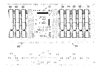
Fig. 1 consists of a plan view and a front view showing a state
in which two motherboards are connected together using a bridging board
according to an embodiment of the present invention;
Figs. 2A and 2B are a plan view and a bottom view respectively
showing a bridging board according to an embodiment of the present
invention;
Fig. 3 is a plan view showing an example of a motherboard;
Fig. 4 is a schematic view depicting non-parallel bus wiring on
a motherboard;
Fig. 5 is a circuit diagram showing the wiring connection
changing circuit configuration of the bridging board; and
Fig. 6 is a table showing wiring connection changing patterns of
the bridging board corresponding to different operational states of
connection change setting selector switches.
DESCRIPTION OF THE PREFERRED EMBODIMENTS
Following is a description of a preferred embodiment of the
present invention with reference to the drawings. Fig. 1 shows an example
in which two motherboards 50 and 60 are connected together using a
bridging board 10 to which the present invention has been applied to form
CA 02356994 2001-09-05
a single motherboard structure. As shown in Fig. 2, the bridging board 10
has a constitution in which an upstream side connector 11 (a plug
connector), a downstream side connector 12 (also a plug connector) and a
system setting IC 15 are provided on the rear face of a substrate 19, and
connection change setting ICs 13 and 14 and connection change setting
selector switches 16 and 17 are provided on the front face.
The motherboard 50 has a constitution in which a system slot
51 positioned at an end thereof and daughter board mounting slots 52 to
58 arranged in a line next to the system slot 51 are provided on a substrate
59. Likewise, the motherboard 60 has a constitution in which a system slot
61 (the no.1 slot) positioned at an end thereof and daughter board
mounting slots 62, 63, 64... arranged in a line next to the system slot 61
are provided on a substrate 69. The motherboard 50 is shown in Fig. 3. In
this example, the motherboard 50 has one system slot (the no. 1 slot) 51
and seven daughter board mounting slots 52 to 58 (the no. 2 to no. 8 slots),
but there may be any number from one to seven daughter board mounting
slots. In other words, each motherboard has a system slot and one or more
daughter board mounting slots, although due to a specification-related
limitation, it is only possible to connect a maximum of seven daughter
board mounting slots per one system slot. Note also that a case in which
daughter boards are not used is also conceivable, in which case the
motherboard will have only the system slot.
When the two motherboards 50 and 60 are connected together
using the bridging board 10 as shown in Fig. 1, the upstream side
connector 11 is fitted into any of the daughter board mounting slots of the
motherboard 50 (in Fig. 1 the no. 6 slot 56), and the downstream side
connector 12 is fitted into the system slot 61 of the motherboard 60. As a
6
CA 02356994 2001-09-05
result, the motherboard 50 becomes the upstream side motherboard and
the motherboard 60 becomes the downstream side motherboard. With this
constitution, a system board is mounted into the system slot 51 of the
upstream side motherboard 50, and daughter boards mounted in the
daughter board mounting slots 52 to 58 of the upstream side motherboard
50 are connected to this system board via bus wiring on the upstream side
motherboard 50 and are controlled by the system board.
Regarding the downstream side motherboard 60, on the other
hand, although only the downstream side connector 12 of the bridging
board 10 is connected into the downstream side system slot 61, due to the
system IC provided on the bridging board 10, signals are received from the
system board provided on the upstream side motherboard 50, which is
connected via the upstream side connector 11, and hence signals are sent
just as if a system board were mounted in the downstream side system slot
61. As a result, daughter boards mounted in the daughter board mounting
slots 62, 63, 64... of the downstream side motherboard 60 are connected
via the bus wiring on the downstream side motherboard 60 to a system
board 'virtually' mounted in the downstream side system slot 61 (i.e. the
system board mounted in the system slot 51 of the upstream side
motherboard 50), and are controlled by this 'virtual' system board. As is
evident from the above, the downstream side connector 12 of the bridging
board 10 must be connected into the system slot of the downstream side
motherboard.
As a result of the above, a state is achieved in which all of the
daughter board mounting slots of both the upstream and the downstream
side motherboards 50 and 60 are controlled by the system board in the
system slot 51 of the upstream side motherboard 50. The two
7
CA 02356994 2001-09-05
motherboards 50 and 60 connected together by the bridging board 10 as
shown in Fig. 1 thus function as a single integrated motherboard
controlled by a single system board. As a result, the number of daughter
board mounting slots can be increased as much as one wishes. Note that,
although in Fig. 1 all of the slots are arranged on the front faces of the
motherboards 50 and 60, a configuration in which a slot into which the
upstream side connector 11 of the bridging board 10 is fitted is provided on
the rear face of the upstream side motherboard 50 and the downstream
side system slot 61 into which the downstream side connector 12 of the
bridging board 10 is fitted is provided on the rear face of the downstream
side motherboard 60, with the bridging board 10 being placed on the rear
face side, is also possible.
If, on the motherboards 50 and 60, the bus wires that connect
the large number of terminals provided in the slots are all parallel wires,
then the bridging board 10 need merely have a plurality of wires that
connect the terminals of the daughter board mounting slot on the
upstream side motherboard into which the upstream side connector 11 is
connected and the terminals of the system slot on the downstream side
motherboard into which the downstream side connector 12 is connected,
following the correspondence relationship therebetween. However, if the
motherboard specifications specify that non-parallel bus wires be provided,
then setting the bridge wiring that connects these non-parallel bus wires
together becomes a problem.
A description of an example of such non-parallel bus wiring will
now be given with reference to Fig. 4. It should be noted that Fig. 4 shows
only an illustrative example of wiring connections that make up non-
parallel bus wiring, and not wiring matching actual specifications. An
s
CA 02356994 2001-09-05
example of non-parallel bus wiring is wiring that connects terminal pins in
A3 positions, B3 positions, C3 positions and E3 positions of the slots 51 to
58 of the upstream side motherboard as in Fig. 4. In Fig. 4, the terminal
pins A3, B3, C3 and E3 are connected in chains using a first bus wire
represented by the double line LA, a second bus wire represented by the
thick line LB, a third bus wire represented by the thin line LC and a fourth
bus wire represented by the broken line LD, with the chains crossing one
another.
Setting is carried out such that interrupt signals INTA, INTB,
INTC and INTD are sent through the non-parallel bus wires LA, LB, LC
and LD respectively. Moreover, according to the specifications, in the
system slot 51, wire LA must be connected to the terminal pin A3 so that
the signal INTA passes therethrough, wire LB must be connected to the
terminal pin B3 so that the signal INTB passes therethrough, wire LC
must be connected to the terminal pin C3 so that the signal INTO passes
therethrough, and wire LD must be connected to the terminal pin E3 so
that the signal INTD passes therethrough. The non-parallel bus wiring
configuration is also similar for the downstream side motherboard 60, and
it is necessary to set the bridge wiring such that the interrupt signals
INTA, INTB, INTO and INTD are connected to the terminal pins A3, B3,
C3 and E3 respectively of the downstream side system slot 61.
It is apparent from the above that when the motherboards 50
and 60 are connected together using the bridging board 10, the connection
of the non-parallel wires LA to LD is a problem. For example, if the
upstream side connector 11 of the bridging board 10 is connected into the
no. 6 slot 56 of the upstream side motherboard 50 as shown in Fig. 1, then
as shown in Fig. 4 the interrupt signals INTD, INTA, INTB, and INTO
9
CA 02356994 2001-09-05
respectively are connected to the terminal pins A3, B3, C3 and E3 of the no.
6 slot 56. However, it is necessary to connect the interrupt signals INTA,
INTB, INTO and INTD respectively to the terminal pins A3, B3, C3 and
E3 of the system slot 61 of the downstream side motherboard 60 which is
connected using the bridging board 10.
Wiring connection changing must thus carried out in the
bridging board 10 such that the interrupt signals INTA, INTB, INTO and
INTD respectively are connected to the terminal pins A3, B3, C3 and E3 of
the downstream side system slot 61. As mentioned earlier, connection
change setting ICs 13 and 14 and connection change setting selector
switches 16 and 17 are provided in the bridging board 10 for carrying out
this wiring connection changing.
The bridge wiring connection changing circuit configuration is
shown in Fig. 5. The connection change setting IC 13 has two input ports
31 (lA, 2A), eight output ports 32 (1B1 to 1B4, 2B1 to 2B4), and two
switching signal ports 33 (S0, S 1), and inside has eight semiconductor
switches 35, a pair of driver circuits 36 and 37, and eight OR circuits 38;
similarly, the connection change setting IC 14 also has two input ports 41
(lA, 2A), eight output ports 42 (1B1 to 1B4, 2B1 to 2B4), and two switching
signal ports 43 (S0, S 1), and inside has eight semiconductor switches 45, a
pair of driver circuits 46 and 47, and eight OR circuits 48; wiring
connections are made as shown in Fig. 5. Moreover, as shown in Fig. 5, the
input ports 31 and 41 (lA, 2A) are connected respectively to the A3, B3, C3
and E3 terminals of the upstream side connector 11, and the output ports
32 and 42 ( 1B 1 to 1B4, 2B 1 to 2B4, 1B 1 to 1B4, 2B 1 to 2B4) are connected
to the A3, B3, C3 and E3 terminals of the downstream side connector 12.
The connection change setting selector switches 16 and 17 are
CA 02356994 2001-09-05
short pin switches; each switch is off when the short pin is removed and on
when the short pin is inserted. As shown in Fig. 5, the switches 16 and 17
are each connected to one of the switching signal ports 33 of the connection
change setting IC 13 and one of the switching signal ports 43 of the
connection change setting IC 14, and are also connected to a power source
line 18 via a resistor. As a result, when the short pin of one of the switches
16 and 17 is removed, an H (high) signal is applied to the corresponding
switching signal ports 33 and 43, and when the short pin is inserted, an L
(low) signal is applied to the corresponding switching signal ports 33 and
43.
As is apparent from the circuit configuration, by changing the
insertion/removal pattern of the short pins of the connection change
setting selector switches 16 and 17, changing of the connections between
the A3, B3, C3 and E3 terminals of the upstream side connector 11 and the
A3, B3, C3 and E3 terminals of the downstream side connector 12 can be
carried out freely. The relationship between the insertion/removal pattern
of the short pins of the connection change setting selector switches 16 and
17 and the connection change setting of the A3, B3, C3 and E3 terminals of
the upstream side connector 11 and the downstream side connector 12 of
the bridging board 10 is shown in Fig. 6. In Fig. 6, the state in which the
short pin of the switch 16 or 17 is inserted is indicated by hatching.
As can be seen from Fig. 6, when, for example, the short pins of
both switches 16 and 17 are inserted, if the interrupt signals INTA, INTB,
INTC and INTD are inputted respectively into the terminal pins A3, B3,
C3 and E3 on the upstream side, then the interrupt signals INTA, INTB,
INTO and INTD are outputted respectively from the terminal pins A3, B3,
C3 and E3 on the downstream side. Similarly, when the short pin of only
11
CA 02356994 2001-09-05
the switch 17 is inserted, if the interrupt signals INTD, INTA, INTB and
INTC are inputted respectively into the terminal pins A3, B3, C3 and E3
on the upstream side, then the interrupt signals INTA, INTB, INTO and
INTD are outputted respectively from the terminal pins A3, B3, C3 and E3
on the downstream side.
If, for example, as shown in Fig. 1, the upstream side connector
11 of the bridging board 10 is fitted into the no. 6 slot 56 of the upstream
side motherboard 50 and the downstream side connector 12 is fitted into
the system slot 61 of the downstream side motherboard 60, then as can be
seen from Fig. 4, the interrupt signals INTD, INTA, INTB and INTO are
inputted respectively into the terminal pins A3, B3, C3 and E3 of the no. 6
slot 56. Finding this pattern in Fig. 6, it can be seen that if the short pin
of
the switch 16 is removed and the short pin of the switch 17 is inserted,
then the interrupt signals INTA, INTB, INTO and INTD will be outputted
respectively from the terminal pins A3, B3, C3 and E3 of the system slot
61 of the downstream side motherboard 60. As a result, the downstream
side motherboard 60 can be integrated with the upstream side
motherboard 50 such that the two function as a single motherboard.
As is apparent from the above, the upstream side connector 11
of the bridging board 10 can be fitted into any of the no.2 to no. 8 slots 52
to
58 (the daughter board mounting slots) of the upstream side motherboard
50. The insertion/removal pattern of the short pins of the connection
change setting selector switches 16 and 17 should be set in accordance
with which of the slots 52 to 58 the upstream side connector 11 is fitted
into, such that the interrupt signals INTA, INTB, INTO and INTD are
outputted respectively from the terminal pins A3, B3, C3 and E3 of the
system slot 61 of the downstream side motherboard 60.
12
CA 02356994 2001-09-05
By using the bridging board 10, any two motherboards can thus
be connected together so as to function as a single motherboard. A
plurality of existing motherboards can thus be freely connected on site
using bridging boards so as to function as a single motherboard. Moreover,
as is apparent from the above description, because semiconductor switches
35 and 45 are used in the bridging board for the connection changing, high
speed signal connection is possible.
If the bridging board according to the present invention is used
as described above, then regardless of what kind of motherboards are used
as upstream side and downstream side motherboards, by connecting the
motherboards together using the bridging board and then suitably setting
the connection switching of the bus wiring using the IC switches, the two
motherboards can be integrated both mechanically and electrically and
used as a single motherboard. It is thus possible to connect together any
plurality of motherboards using bridging boards according to the present
invention to easily construct a single motherboard having a large number
of daughter board mounting slots.
The invention being thus described, it will be obvious that the
same may be varied in many ways. Such variations are not to be regarded
as a departure from the spirit and scope of the invention, and all such
modifications as would be obvious to one skilled in the art are intended to
be included within the scope of the following claims.
RELATED APPLICATIONS
This application claims the priority of Japanese Patent
Application No. 2000-274896 filed on September 11, 2000, which is
13
incorporated herein by reference.
14