Note: Descriptions are shown in the official language in which they were submitted.
76909-95E
CA 02357070 2001-09-05
1
A METHOD FOR DETECTING THE PRESENCE OF ROBBED-BIT SIGNAI~I~ING
This application is a divisional of copending
Canadian Patent Application No. 2,261,635 filed February 19,
1998 in the name of Brent Townshend.
BACKGROUND OF THE INVENTION
The field of the present invention pertains
generally to data communications equipment, and more
particularly to a device for transmitting digital data over
a telephone connection.
Data communication plays an important role in many
aspects of today's society. Banking transactions,
facsimiles, computer networks, remote data base access,
credit-card validation, and a plethora of other applications
all rely on the ability to quickly move digital information
from one point to another. The speed of this transmission
directly impacts the quality of these services and, in many
cases, applications are infeasible without a certain
critical underlying capacity.
At the lowest levels, most of this digital data
traffic is carried over the telephone system. Computers,
facsimile machines, and other devices frequently communicate
with each other via regular telephone connections or
dedicated lines which share many of the same characteris-
tics. In either case the data must first be converted into
a form compatible with a telephone system designed primarily
for voice transmission. At the receiving end the telephone
signal must be converted back into a data stream. Both
tasks are accomplished by modems.
4
' 76909-95E
CA 02357070 2001-09-05
2
A modem performs two tasks corresponding to the
needs above: modulation, which converts a data stream into
an audio signal that can be carried by the telephone system,
and demodulation, which takes the audio signal and recon-
structs the data stream. A pair of modems, one at each end
of a connection, allows bidirectional communication between
the two points. The constraints on the audio signal create
the limitations on the speed at which data can be trans-
ferred using modems. These constraints include a limited
bandwidth and degradation of data by noise and crosstalk.
The telephone system typically can carry only signals that
range in frequency between 300 Hz and 3,400 Hz. Signals
outside this range are sharply attenuated. This range was
built into the design of the telephone system since it
covers a significant portion of the human voice spectrum.
However, the bandwidth of a channel is one factor that
determines the maximum attainable data rate. With all other
factors constant, the data rate is directly proportional to
the bandwidth.
Another factor is the distortion of the audio
signal or any other signal that the communications endpoints
cannot control. This includes electrical pickup of other
signals being carried by the telephone system (crosstalk),
electrical noise, and noise introduced by conversion of the
signal from one form to another. The last type will be
expanded upon in later discussion.
For general utility, modems are designed to be
operable over most telephone connections. Thus, they must
be designed for worst-case scenarios, which include band-
width limitations and significant noise that cannot be
CA 02357070 2002-03-20
76909-95E
2a
removed. Even so, substantial progress has been made on
modem design in the past several yeaws. Devices capable of
operating at speeds up to 28,800 bits per second are now
commonly available. See International Telecommunication
S Union, Telecommunication Standardization Sector (ITU-T),
Recommendation V.34, Ge:ne:va, Switzerland (1994). However,
theoretical arguments based on i:he channel bandwidth and
noise levels show that t~.e maximum possible speed has nearly
been obtained and further significant increases are highly
unlikely with the given constraints. This is discussed in
C.E. Shannon, "A Mathematical theory of Communication," Bell
System Technical Journal 27:379--423, 623-656 (1948).
Unfortunately, although speeds approaching 30,000
bits per second (or 3,6~;)U bytes per second) make many data
communications applications feasible, conventional modem
transmission is still not fast. Enough for all uses. At
these speeds, transmiss.~_on of text is fast, and low-quality
audio, such as digitized speech, is acceptable. However,
facsimile or still-image transmission is slow, while high-
quality audio is limited and full-motion video has not been
satisfactorily achieved. In short, what is needed is
greater data transmission capability. This is a prere-
quisite for the new applications and is ,a necessity for
maximizing the performance of many existing applications.
Of course the telephone companies, cable-
television providers, arnd others are not ignorant of these
increasing data transmission needs. One approach to
providing higher speed data connections vo businesses and
residences is to provide end-to-end digiv al connectivity,
eliminating the need for additional modems. One offering of
CA 02357070 2001-09-05
' 76909-95E
2b
such a service is the Integrated Services Digital Network
(ISDN). See: International Telecommunication Union,
Telecommunication Standardization Sector (ITU-T), "Inte-
grated Services Digital Networks ISDNs," Recommendation I.
120, Geneva, Switzerland (1993), and John Landwehr, "The
Golden Splice: Beginning a Global Digital Phone Network,"
Northwestern University (1992). ISDN replaces the existing
analog local loop with a 160,000 bit/second digital connec-
tion. Since the bulk of long-distance and inter-office
traffic is already carried digitally, this digital local
loop can be used
CA 02357070 2001-09-05
3
for end-to-end digital voice, computer data or any other type of information
transfer. However, to
achieve these data transmission rates on the local loop, special equipment
must be installed at both
ends of the line. Indeed, the entire telephone network is currently undergoing
a transformation from a
voice transmission network to a general data transmission service, with voice
just being one particular
form of data.
Once installed, each basic ISDN link will offer two data channels capable of
64,000
bits/second, a control channel with a capacity of 16,000 bits/second, reduced
call connection time,
and other benefits. At these rates, facsimile and still image transmission
will be nearly instantaneous,
high-quality audio will be feasible, and remote computer connections will
benefit from a fivefold
speed increase. Some progress toward full-motion video may also be achieved.
The down side of ISDN is its availability or lack thereof. To use ISDN, the
user's central
office must be upgraded to provide this service, the user must replace its on-
premises equipment
(such as telephones) with their digital equivalents, and each individual line
interface at the central
office must be modified to canry the digital data stream. This last step, the
conversion to a digital link
of the millions of analog connections between every telephone and the central
office, is formidable.
The magnitude of this task dictates that the deployment of ISDN will be slow
and coverage will be
sporadic for some time to come. Rural and sparsely populaxed areas may never
enjoy these services.
Another existing infrastructure potentially capable of providing high-speed
data
communications services is the cable television system. Unlike the telephone
system, which connects
to users via low-bandwidth, twisted-pair wiring, the cable system provides
high-bandwidth
connectivity to a large fraction of residences. Unused capacities on this
wiring could provide data
rates of tens, or even hundreds, of millions of bits per second. This would be
more than adequate for
all of the services envisioned above including full-motion digital video.
However, the cable system
suffers from a severe problem --- its network architecture. The telephone
system provides point-to-
point connectivity. That is, each user has full use of the entire capacity of
that user's connection---it is
not shared with others and does not directly suffer due to usage by others.
The cable system on the
other hand, provides broadcast connections. The entire capacity is shared by
all users since the same
signals appear at each user's connection. Thus, although the total capacity is
high, it is divided by the
number of users requiring service. This architecture works well when all users
require the same data,
such as for cable's original design goal, television distribution, but it does
not serve well a community
of users with different data needs. In a metropolitan area the data capacity
available to each user may
be significantly less than via an ISDN or modem connection.
CA 02357070 2001-09-05
' 76909-95E
4
To provide high-speed, data connectivity to a
large number of users, the cable system could be modified to
isolate different segments of the user population effec-
tively sharing the cable bandwidth over smaller populations.
However, like ISDN, this will be a slow, costly process that
will provide only partial service for many years to come.
The methods used to design modems are based
largely on models of the telephone system that have remained
unchanged for several decades. That is, a modem is modeled
as an analog channel with a finite bandwidth (400-3400 Hz)
and an additive noise component on the order of 30 dB below
the signal level. However, a large portion of the telephone
system now uses digital transfer of a sampled representation
of the analog waveforms for inter-office communications. At
each central office, the analog signal is converted to a
64,000 bit/second pulse code modulated (PCM) signal. The
receiving office then reconstructs the analog signal before
placing it on the subscriber's line. Although the noise
introduced by this procedure is to a first approximation,
similar to that observed on an analog system, the source of
the noise is quite different. See K. Pahlavan and J.L.
Holsinger, "A Model for the Effects of PCM Companders on the
Performance of High Speed Modems," Globecom '85, pages 758-
762 (1985). Most of the observed noise on a telephone
connection that uses digital switching is due to quantiz-
ation by the analog-to-digital converters needed to convert
the analog waveform into a digital representation.
As noted above, most telephone connections are
currently carried digitally between central offices at rates
of 64,000 bits/second. Furthermore, ISDN services demon-
strate that it is possible to transmit significantly more
CA 02357070 2001-09-05
' 76909-95E
than these rates over the local loop. It has been suggested
that it may be possible to design a transmission scheme that
takes advantage of these factors. Kalet et al. postulate a
system, shown in Figure 2, in which the transmitting end
5 selects precise analog levels and timing such that the
analog-to-digital conversion that occurs in the trans-
mitter's central office might be achieved with no quantiza-
tion error. I. Kalet, J.E. Mazo, and B.R. Saltzberg, "The
Capacity of PCM Voiceband Channels," IEEE International
Conference on Communications '93, pages 507-511, Geneva,
Switzerland (1993). By making use of the mathematical
results of J.E. Mazo it is conjectured that it should be
theoretically possible to reconstruct the digital samples
using only the analog levels available at the receiver's end
of the second local loop in the communications path. J.E.
Mazo, "Faster-Than-Nyquist Signaling," Bell System Technical
Journal, 54:1451-1462 (1975). The resulting system might
then be able to attain data rates of 56,000 to 64,000
bits/second. The shortcoming of this method is that it is
nothing more than a theoretical possibility that may or may
not be realizable. Kalet et al. state that "This is a hard
practical problem and we can only conjecture if a reasonable
solution would be possible." Id. at page 510.
An example of a conventional attempt to solve the
foregoing problem is found in work by Ohta, described in US
Patent Numbers 5,265,125 and 5,166,955. Ohta disclosed an
apparatus to reconstruct a PCM signal transmitted through a
communications channel or reproduced from a recording
medium. These patents "exemplify some conventional tech-
niques abundant in the literature to deal with the general
CA 02357070 2001-09-05
' 76909-95E
5a
problem of reconstructing a multi-valued signal that has
passed through a distorting channel." See also, for example,
Richard D. Gitlin, Jeremiah F. Hayes and Stephen B.
Weinstein, ~~Data Communications Principles," Plenum (1992).
However, such conventional teachings do not consider the
application of methods to handle the output from a nonlinear
quantizer, nor do they deal with the specific problems of
decoding digital data passed over a telephone local loop.
Furthermore, the problem of reconstructing a sampling rate
clock from the PCM data is non-trivial when the PCM signal
can take on more than two values. For example, in the
patents by Ohta, a simple clock recovery system which relies
on a binary input signal is employed. This type of clock
recovery cannot be used with the multivalued codes used in a
telephone system. Also, compensation for drift with time
and changing line conditions requires use of an adaptive
system which the prior art of PCM reconstruction does not
include.
Thus, there is currently a critical disparity
between the required or desired data communications capacity
and that which is available. Existing modems do not provide
adequate capacities, and new digital connectivity solutions
are several years away from general availability. Refitting
the existing infrastructure with ISDN capability is a siz-
able task and may take a decade before its use is wide-
spread. A new method of data transmission could immensely
benefit many current applications as well as making several
new services available which would otherwise have to wait
until the infrastructure catches up with the requirements.
CA 02357070 2001-09-05
' 76909-95E
5b
Accordingly, there is a need for providing a new
system of data transfer which provides the capability to
receive data at high rates over existing telephone lines.
There is also a need for an improved system of
data transfer which can enable systems, equipment, and
applications designed for a digital telephone system (such
as ISDN) to be used with analog connections.
CA 02357070 2001-09-05
6
There is also a need for an improved system of data transfer which is capable
of taking
advantage of the digital infrastructure of the telephone system without
requiring costly replacement of
all subscribers' lines.
It also would be desirable to create a high speed communication system to
provide a means
to distribute high-quality digital audio, music, video, or other material to
consumers. Such an
improved system of data transfer would advantageously provide a means to
distribute, on-demand,
individually-tailored information, data, or other digital material to a large
number of consumers.
There is also a need for an improved high speed communications system to
provide greater
throughput for commercial applications such as facsimile, point-of sale
systems, remote inventory
management, credit-card validation, wide-area computer networking, or the
like.
SUMMARY OF THE INVENTION
15 One aspect of the present invention comprises a system for transferring
data over existing
telephone connections at rates higher than known modems or conventional
methods of data
transmission. The present invention achieves a significant improvement over
conventional methods
by making use of two critical observations:
1. The underlying phone system is digital using PCM transmission.
20 2. High data rates are required in one direction only, the sowce of which
has direct
digital access to the telephone system.
An aspect of the present invention utilizes the foregoing observations to
achieve higher data
transmission rates than were previously attainable with conventional systems.
The second
25 observation above addresses the largest use of modems --- to access and
retrieve information from
centralized servers. In addition, the present invention has been found
particularly useful for
applications that require higher data rates, such as database access and video
or audio on demand.
Such applications can be realized, utilizing the high data transmission rates
that a~ attainable through
the present invention.
An important aspect of the invention is both simple and extremely powerful;
that is, to allow
the data provider to connect directly to a digital telephone network while the
consumer uses its
existing analog connections without change to the line. This configuration
grcatly changes the model
under which the consumer's data equipment must operate. Existing modems must
deal with
bandwidth limitations and multiple unidentified noise sources that corrupt a
signal over the entire
CA 02357070 2001-09-05
transmission path. In contrast, an aspect of the present invention carries
data digitally over the bulk
of the path, from the central office to the consumer's home or office, and
converts it to analog form
only for the last segment of that path. Advantageously, one of the primary
sources of noise to
existing modems, quantization noise during analog-to-digital conversion, is
completely eliminated
since such conversion is no longer required. Furthermore, quantization noise
during digital-to-analog
conversion, can be modeled as a deterministic phenomenon, and thus
significantly reduced.
By using the foregoing aspect of the invention, the data source, which has
direct access to the
digital network (for example, by ISDN), can transfer exact data to the central
office serving the
consumer of the data. All that is then required is a device at the consumer's
end of the local loop that
will compensate for distortion of the data signal due to the filtering
performed at the central office's
digital-to-analog converters and due to the transmission line. Both
distortions can be dealt with
adequately using existing digital signal processing hardware, as will be
described herein.
Note that although this method cannot be used for return data from the
consumer to the
server, existing modems can be used, giving an asymmetrical channel with a
capacity of up to 64,000
bits/second from server to consumer and 20,000 to 30,000 bits/second return.
It will be appreciated that an aspect of the invention enables digital data of
any type (audio,
video, information, or the like) to be sent to individual users at speeds
higher than can be obtained
with conventional modems, or conventional methods of data transfer.
Furthermore, unlike cable
television distribution systems, this invention can service, at the full data
rate, any number of users
simultaneously requesting different data.
Beyond providing greater speed of operation for existing applications, such as
remote
computer access, high-speed facsimile transmission, etc., certain aspects of
the invention make
several new applications possible. These include high-quality audio or music
transmission, video-on-
demand, still picture transmission, videophone, teleconferencing, or like
applications in which high
data transmission rates are essential.
Another aspect of the present invention is to reconstruct a multivalued PCM
data signal from
an analog representation of that signal. This is achieved using a new method
which combines a novel
clock synchronization technique with adaptive equalization.
CA 02357070 2001-09-05
76909-95E
8
In addition to the foregoing, other aspects and
advantages of the present invention include: (1) the ability
to effectively reconstruct the telephone system's digital
pulse-code-modulated (PCM) data stream using only the analog
signal at the subscriber end of the telephone line; (2) the
ability to reconstruct the clock frequency and phase of the
PCM data, using only the analog signal at the subscriber end
of the telephone line; (3) the ability to increase the
effective data rate between a central office and the sub-
scriber end without adding additional equipment at the
central office or otherwise modifying the telephone system
and (4) the ability to reconstruct said digital data after
such data had been modified due to one or more of conversion
to analog form, filtering, distortion, or corruption by the
addition of noise.
The invention may be summarized in a communication
system that includes an encoder and a decoder, wherein the
encoder has a digital connection to a digital portion of a
telephone network and the digital portion of the telephone
network is connected by an analog loop to the decoder,
wherein the analog loop converts digital information from
the network into analog voltages for transmission to the
decoder, a method of detecting the presence of robbed-bit
signaling within the digital portion of the telephone
network comprising the steps of: sending a predetermined
pattern of PCM codewords from the encoder to the digital
portion of the telephone networks receiving said predeter-
mined pattern of PCM codewords in the form of analog
voltages at the decoder; determining an error measurement at
the decoder in response to said received analog voltages;
CA 02357070 2002-06-18
76909-95E
8a
and determining whether robbed-bit signaling is present
based upon said error measurement.
Preferably, the error measurement determining step
includes comparing said received analog voltages to
predetermined reference voltages.
BRIEF DESCRIPTION OF DRAWINGS
These and other features, aspects and advantages
of the present invention will become better understood with
regard to the following descriptions, appended claims and
accompanying drawings in which:
Figure 1 is a block diagram showing a typical
modem data connection;
Figure 2 is a block diagram showing an example of
a hypothetical symmetric digital system;
Figure 3 is a block diagram showing a high speed
distribution system in accordance with an aspect of the
present invention
Figure 4 is a block diagram of a hardware
implementation of an encoder 150 of Figure 3, in accordance
with an aspect of the present invention:
Figure 5 is a block diagram showing the function
of encoder 150 of Figure 3, in accordance with an aspect of
the present invention;
Figure 6 is a block diagram showing the function
of a DC eliminator 184 of Figure 5, in accordance with an
aspect of the present invention;
CA 02357070 2002-06-18
76909-95E
8b
Figure 7a is a graph of a data stream 100 as a
function of time, such as would be applied to encoder 150 in
accordance with an aspect of the present invention;
CA 02357070 2001-09-05
9
Figure 7b is a graph of a typical output from encoder 150 as a function of
time, such as would
be applied to a digital network connection 132 of Figure 3, in accordance with
an aspect of the
present invention;
Figure 7c is a graph of a linear value 194 of Figure 6 as a function of time,
this is the output
signal from encoder 150 after conversion to linear form, in accordance with an
aspect of the present
invention;
Figure 8 is a block diagram showing the function of existing digital line
interfaces, for
reference in understanding an aspect of the present invention;
Figure 9 is a block diagram of a hardware implementation of a decoder 156
shown in Figure
3, in accordance with an aspect of the present invention;
Figure 10 is a block diagram showing the function of decoder 156 of Figure 3,
in accordance
with an aspect of the present invention;
Figure 11 a is a graph of an analog signal 154 of Figure 10 as a function of
time, in
accordance with an aspect of the present invention;
Figure 11 b is a graph of a compensated signal 2 74 of Figure 10 as a function
of time, formed
within decoder 156 in accordance with an aspect of the present invention;
Figure 11 c is a graph of an estimated code stream 280 of Figure 10 as a
function of time,
formed within decoder 156 in accordance with an aspect of the present
invention;
Figure l 1 d is a graph of a data stream 126 of Figure 3 as a function of
time, generated by
decoder 156 in accordance with an aspect of the present invention;
Figure 11 a is a graph of an error signal 272 of Figure 10 as a function of
time, generated by
decoder 156 in accordance with an aspect of the present invention;
Figure 12 is a block diagram showing an inverse filter 268 of Figure 10, in
accordance with
an aspect of the present invention;
CA 02357070 2001-09-05
Figure 13 is a block diagram showing a feed-forward equalizer 300 of Figure
12, in
accordance with an aspect of the present invention;
Figure 14 is a block diagram showing a filter tap 330 of Figure 13, in
accordance with an
5' aspect of the present invention;
Figure 15 is a block diagram showing a clock estimator 264 of Figure 10, in
accordance with
an aspect of the present invention;
10 Figure 16 is a block diagram showing the function of a clock synchronizer
260 of Figure 10,
in accordance with an aspect of the present invention;
Figure 17 is a block diagram showing an end-to-end asymmetric system with a
reverse
channel in accordance with an aspect of the present invention;
Figure 18 is a block diagram showing an application of an aspect of the
present invention
with a database server;
Figure 19 is a block diagram showing an aspect of the present invention in an
application to a
high speed facsimile system;
Figure 20 is a block diagram showing a digital telephony relay in accordance
with an aspect
of the present invention.
CA 02357070 2001-09-05
11
DETAILED DESCRIPTION OF THE PREFERRED. EMBODIMENTS
Conventional Modem Data Connection
A conventional modem data connection is shown in Figure 1. Operation of such a
system is
well known and has been standardized by government agencies such as the
International
Telecommunications Union. Depending on the types of a modem 104 and a modem
124, data may be
applied at rates of up to 28,800 bits/second via the first user's data stream
100. Modem 104 converts
data stream 100 into an analog signal, which is applied to a local loop 106,
which in turn connects to a
telephone switch 108. The analog signal is then carried through a telephone
network 114 via a
network connection 112 and eventually reaches, via a network connection 118, a
telephone switch
120 serving the second user. The signal is then passed, in analog form, via a
local loop 122 to the
second user's modem 124, which converts the signal to data stream 126, which
will be a delayed
version of data stream 100. In an exactly analogous way, a data stream 128
travels through the
telephone network via modem 124, local loop 122, telephone switch 120, a
network connection 116,
telephone network 114, a network connection 110, telephone switch 108, local
loop 106, and modem
104 to form a delayed version as a data stream 102.
This system assumes that the telephone system reproduces the analog signal,
applied at one
user's telephone connection, at the other user's end with distortion and delay
not greater than a set of
standard values specified for the telephone system. One can show that, based
only on these values, it
is not possible to transmit data at rates greater than approximately 35,000
bits/second. This system
ignores many details of the distortion, which may, in fact, be deterministic
changes to the signal
rather than unpredictable changes. One such deterministic change is
quantization noise if telephone
network 114 is implemented digitally. Existing modems cannot make use of
knowledge of this
significant noise source in eliminating distortion and are thus limited in
their data rates. This is the
key shortcoming of existing modem systems --- low data rate and a theoretical
limit on the maximum
improvement that will ever be possible within the current framework of
assumptions.
In an attempt to overcome the foregoing shortcomings and disadvantages of a
conventional
modem data connection as shown in Figure 1, an approach to increasing the rate
of data transfer has
resulted in a hypothetical symmetric digital communication system, Such a
system is shown in
combination with a digital telephone network in Figure 2.
CA 02357070 2001-09-05
12
This system, described by Kalet et al. in the previously cited reference, is
similar to existing
modems but with a new assumption; that the underlying infrastructure is a
digital telephone network
134. The operation is similar to that of the conventional modem system
described above except that
the signals are carried-in digital form within digital telephone network 134
and on a digital network
connection 130, digital network connection 132, a digital network connection
136, and a digital
network connection 138. Each user still requires a modem to transfer the
information via local loop
122 and local loop IOG to telephone switch 120 and telephone switch 108
respectively where
conversion between analog and a standard digital format used by digital
telephone network 134 is
performed. '
Unlike conventional modems, no theoretical argument has yet been found which
would limit
the speed of such a system to less than that used internally within digital
telephone network 134,
typically 56,000 or 64,000 bits/second. Thus, it is hypothetically possible
that such a system could
obtain data rates up to 64,000 bits/second. However, such a system has never
been reduced to
practice nor is there any evidence that it would be possible to implement such
a system. The authors
of this system state that "This is a hard practical problem and we can only
conjecture if a reasonable
solution would be possible. "
The problem is that to make use of the knowledge that the underlying network
is digital and a
large part of the observed signal distortion is due to quantization noise, the
transmitting modem must
control, via only its analog output, the digital Levels chosen by the network
to encode the signal.
Furthermore, the receiving modem must, via only its analog input, accurately
infer those digital
levels. Distortion due to analog/digital conversion occurs at both the
transmitter and receiver's end
yet only the combined distortion added to the desired signal is directly
observable. Furthermore,
additional distortion due to electrical noise and crosstalk also occurs on
local loop 122 and local loop
106. Separating out these distortion components from the desired signal and
each other is a difficult,
perhaps impossible, task.
One aspect of the present invention is a method by which the shortcomings of
this approac«
are eliminated. It makes use of knowledge of the underlying digital network in
a way that is
realizable, providing higher attainable data rates than possible with any
other known solution.
CA 02357070 2002-03-20
76909-95E
Sampling Rste Conversfoa
i3
As will be seen in subsequent discussion, a system fa recovering PCM data 6nm
a distorted
analog reprtscntation-requires a mctlwal of synchronizing the decoding clock
with that used to convert
!l the PCM data froth a digital stream to analog values. Digital
implementations of this synchronization
require that a digital data sequence be reaarrtpled, changing its rate from
that used by as analog-to-
digital converter to one which is closer to that used in conversion from PCM
data. Previously Zmown
techniques for achieving this are either strictly limited its their
capabilities, or are computationally
intensive. See, for example,1ZE. Crochiere and L.R- Rabina~. "MuJtitrate
Digital Signal
t I) Pro~.sin&"Prentice-Hall. Englewood Clit~'s, NJ, 1y83 .
Perforating sampling rate conversion betanrn two mdependatt clocks whose
relatiotrship
may change as a function of tithe finrtlrer c:omplicatex the ta:ac.
One aspect of the prcsertt invention is a method which can perform such
conversion with a
minimum of computational overhead, at accepts a continuously-variable
input/output sampling rate
ratio and performs the conversion with high accuracy. The techniques described
can obtain greater
than 90dB anti-abasing rejection and can be implemented au real-time on
existing processors.
Ovetai! System
20 Figure 3 shows an overview of the proposed systtm. The method of use of the
system strum
in Figure 3 is identical to that far current data communications circuits err
modems. Dam applied at
data stream 100 will appear some time later at data strann 126. Data stream
100 to applied to
encoder 150 whose function is to catvert the data strain into a format
compatible with the telephone
system. The converted data is applied to digital telephone network 134 via
digital network
2~,5 cormection 132. The converted data emerges verbatim via diptal a~etwork
cor>:rection 138 at a cliatCs
telephone central office where a line initrface 140 is located. At this point,
if the client also had
direct digital access to the digital cmratection to the clunt's line from
digital xtvroric
connection 138, the ttansmission~would Re complete. However, where the client,
lt7cc the majority of
users, does not have direct digital access to the telcphoite r~t~rork, this is
not possible, and the
'.30 following additional operations art ttduired.
Line interlace l40 converts the digital data on digital network cormectio<t
138 into an analog
form in a manner conforming to the standardized specificxtiaes of digital
telephony. The analog form
is carried on local loop 122 to the client'~r premises where a hybrid network
152 terminates the line
35 and produces analog signal 154. Hybrid network 1 i2 is a standard part
which converts the two-wirt
CA 02357070 2001-09-05
14
bi-directional signal to a pair of one-way signals. Decoder 156 uses analog
signal 154 to estimate and
compensate for the distortion introduced by the conversion to analog form
performed by Line interface
140, resulting in an estimate of the digital data at digital network
connection 138, which is assumed to
be identical to the digital data that was applied at digital network
connection 132. The transformation
performed by encoder 150 is then inverted and decoder 156 outputs data stream
126, which is delayed
estimate of the original data stream 100.
Note that within Figure 3, all elements are well known and exist within
current digital
telephone systems except encoder 150 and decoder 156, which will be described
in detail below.
Also to be described below, is a method of initializing and adapting decoder
156 to the exact
conditions encountered in normal operation.
Physical Implementation Of Encoder
Figure 4 shows a block diagram of one possible realization of encoder 150 of
Figure 3. Data
stream 100 from Figure 3 is applied to the serial data input of a digital
signal processor 160 such as an
AT&T DSP32C. This processor uses a processor bus 162 to communicate with a
read-only memory
168, a random access memory 166, and an ISDN interface circuit 164 such as an
Advanced Micro
Devices Am79C30A. Read-only memory 168 contains a stored-program whose
functional
characteristics will be described in following sections. Random access memory
166 is used for
program storage and parameters. ISDN interface circuit 164 also has an ISDN
connection 170, which
is connected to a network terminator 172, such as Northern Telecom NTI, and
subsequently to digital
network connection 132, which was also shown in Figure 3.
To produce a fully-functional implementation, additional secondary elements
such as
decoders, oscillators, and glue logic would need to be added to the basic
block diagram shown in
Figure 4. Such additions are well known and will be evident to those skilled
in the art.
Subsequent discussion of encoder 150 will refer to functional rather than
physical
components, all of which can, for example, be implemented as programs or
subroutines for digital
signal processor 160 using well-known digital signal-processing techniques.
CA 02357070 2001-09-05
Encoder Operation
Figure 5 shows a functional block diagram of encoder 150 of Figure 3. The
channel from
5 server to client begins with arbitrary digital data provided as data stream
100. Encoder 150 converts
this bitstream into a sequence of eight-bit words sampled, preferably, at the
telephone system's clock
rate of 8,000 samples/second. This is achieved by a sequence of operations
beginning with a serial-
to-parallel convener 180, which groups together each eight bits read from data
stream 100, outputting
a stream of parallel eight-bit values as an 8-bit code stream 182. This
mapping may preferably be
10 performed such that the first of each eight bits read from data stream 100
is placed in the least-
significant bit position of 8-bit code stream 182 with subsequent bits
occupying consecutively more
significant bit positions until the output word is complete, at which point
the process repeats. DC
eliminator 184 then inserts additional eight-bit values at regular intervals,
preferably once per eight
samples, such that the analog value associated with the inserted value is the
negative of the sum of all
15 prior values on 8-bit code stream 182. This is necessary since telephone
systems frequently attenuate
or remove any DC bias on a signal. DC eliminator 184 is one example of a
circuit means for reducing
DC components in the received analog signal.
A detail of the functional elements of DC eliminator 184 of Figure 5 is shown
in Figure 6. A
~ code stream 186 output from a two-input selector 190 is also converted to
linear value 194 by a ~-
law-to-linear converter 192, which can be implemented as a 256-element lookup
table using the
standard p-law-to-linear conversion table. Values of linear value 194 are
accumulated and negated by
a summer 196 and a unit delay 200 to form a DC offset 198 and a previous DC
offset 202, which is
the corresponding unit-delayed value. DC offset 198 is applied to a linear-to-
u-law converter 204,
which can use the same lookup table as p-law-to-linear converter 192, but
performing the inverse
mapping. Note that if DC offset 198 is greater than or less than the maximum
or minimum value in
the table, the respectively largest or smallest entry will be used. A DC
restoration code 206 is
produced by linear-to-p -law converter 204 and applied as one input to two-
input selector 190. Two-
input selector 190 operates by reading, preferably seven, sequential values
from 8-bit code stream 182
and outputting these values as code stream 186, followed by reading and
outputting a single value
from DC restoration code 206. It then repeats this sequence of operations
continually.
Returning to Figure 5, code stream 186 is applied to the input lead of an ISDN
converter 188,
which provides the well-known conversion to an ISDN signal. The function of
ISDN converter 188 is
implemented directly by several existing integrated circuits, including an
Advanced Mcro Devices
CA 02357070 2002-03-20
76909-95E
16
Am79C30. The output of ISDN converter 18$ forms digital network cmtnection
132, which is also
the output of encoder I50 of Figurc 3.
For further understanding, some o:f the signals used by encoder 150 are
illustrated in Figures
!6 7a through 7c. Figure 7a shows a sequence of samples of data stream 100.
After processing by
serial-to-parallel converter I80 and DC eliminator 184, code stream 186 is
shown in Figure 7b.
Within DC eliminator 184, the linear equivalent of code stream 186, namely
linear value 194, is
shown in Figure 7c.
1 n Line Interface
For reference during subsequent descriptions, Figure 8 shows a functional
model of line
interface 140 of Figure 3, such as would bye found in a typical telephone
system for use with an aspect
of the present invention. Note that such interfaces are well known and are
currently used in digital
1 !5 telephone switches. Digital telephone network 134 of Figure 3 passes an
eight- bit-per-sample, p-
law-encoded, digital data-stream via digital network connection 138 to a lt-
law-to-linear convtrtet
210, shown in Figure 8. N-law-to-linear converter 210 implements the well-
known lt-law-to-liruar
conversion, converting each sample to a linear value :212. Linear value 212 is
then converted to an
analog signal 216 by a digital-to-analog converter 214 that is sampled using a
telephone system clock
2n 236 in a well known momter. Although not shown in Figure 3 for reasons of
clarity, telephone system
clock 236 is generated by digital telephorna network 134. Analog signal 216 is
then smoothed by a
lowpass filter 218 to form a filtered signal 220. The main purpose of lowpass
filter 218 is to provide
a low-pass fiutetion with a cutoff frequ~nc~r of approximately 3100 Hz. The
International
Telecommunications Union has standardised the specifications for digital-to-
analog converter 214
25 and lowpass filter 218 in International "telecommunication
Union,'telecommunication
Standardization Sector (ITV-T), "Tranxmcssion Performance Characteristics of
Parlse Code
Modulation," Recommendation G. 7I2, (ieneva, Switzerland, September 1992..
30 Filterod signal 220 is multiplexed onto local loop 122 by a four-to-two-
wire converter Z22.
Local loop 122 is bi-directional; incoming signals on local loop 122 are
applied to four-to-two-wire
converter 222 and are output as an unfiltered signal 234. Unfiltered signal
234 is applied to a
bandpass filter 232, which has also been standardized by ITU-T in the about
cited reference. The
output from bandpaas filter 232, a filtered signal 230, is conversed too
linear value 226 by an analog-
3 6 to-digital converter 228. Linear value 226 is then converted to digital
network connection 136 by a
CA 02357070 2001-09-05
linear- to p-law converter 224, which implements the standard linear-to-u-law
conversion. Note that
in the system shown in Figure 3, digital network connection 136 is not used
and has been omitted for
clarity.
Physical Implementation of Decoder
Figure 9 shows a block diagram of one possible realization of decoder 156 of
Figure 3.
Analog signal 154 from Figure 3 is sampled by an analog-to-digital converter
240, which exists as an
integrated circuit, such as a Crystal Semiconductor CS5016. This uses a clock
signal 244, preferably
at 16 kHz, generated by an oscillator 242, to form a digital input signal 246,
which is connected to a
bank of digital signal processors 248, such as AT&T DSP32C's, via one of their
serial digital input
leads. The processors are also connected to each other and to a random access
memory 254 and a
read-only memory 252 via a processor bus 250. Read-only memory 252 contains a
stored-program
whose functional characteristics will be described in following sections. Bank
of digital signal
processors 248 produces data stream 126, which is the final output of decoder
156 of Figure 3.
To produce a fully-functional implementation, additional secondary elements
such as
decoders, oscillators, and glue logic would need to be added to the basic
block diagram shown in
Figure 9. Such additions are well known and will be evident to those skilled
in the art.
Subsequent discussion of decoder 156 will refer to functional rather than
physical
components, all of which can, for example, be implemented as programs or
subroutines for the bank
of digital signal processors 248 using well-known digital signal-processing
techniques.
Decoder Operation
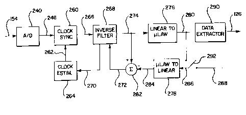
Figure 10 shows the functional structure of decoder 156 of Figure 3. Analog
signal 154 from
Figure 3 provides the.input data to decoder 156. Analog signal 154 is fed to
analog-to-digital
converter 240 and convened to digital input. signal 246, preferably sampled at
16,000 samples per
second with 16 bits per sample precision. Analog-to-digital converter 240
exists as an integrated
circuit, such as a Crystal Semiconductor CS5016. Digital input signal 246 is
then processed by clock
synchronizer 260 which interpolates and re-samples digital input signal 246 at
intervals separated by
a period estimate 262 to produce a synchronized signal 266. The operation of
clock synchronizer 260
will be detailed in following sections. Synchronized signal 266 is filtered by
inverse filter 268, which
will be described below, to reconstruct compensated signal 274. The purpose of
inverse filter 268 is
CA 02357070 2001-09-05
to invert the transformation performed by line interface 140 of Figure 3 of
which the primary
component is lowpass filter 218 of Figure 8. Returning to Figure 10, inverse
filter 268 also outputs a
delay error estimate 270 giving the timing error inherent in synchronized
signal 266, which will be
used by clock estimator 264, described below, to compute the period estimate
262 used by clock
synchronizer 260. A decision means is then used to convert compensated signal
274 to a sequence of
values from a discrete set. As an example, compensated signal 274 is converted
to the nearest
equivalent eight-bit p-law word using a linear-to-p-law converter 276 to give
estimated code stream
280. As described earlier, linear-to-p-law converter 276 may be implemented as
a simple lookup
table.
1C
During normal operation, a switch 292 gates estimated code stream 280 back as
a desired
output signal 286, which is converted back to a linear signal by a ~-law-to-
linear converter 278 to
form a linear value 284, u-law-to-linear converter 278 can be implemented as a
simple lookup table
as earlier described. During initialization, switch 292 will be set such that
a predetermined training
15 pattern 288 (not shown in Figure 3) is gated to desired output signal 286.
This usage will be
described below.
Linear value 284 provides an estimate of the desired value of compensated
signal 274. It is
used to adaptively update inverse filter 268 such that compensated signal 274
is as close as possible to
20 linear value 284. This adaptation is one example of a training means for
adjusting the parameters of
decoder 156, which will be further explained in the discussion of inverse
filter 268 below. A
subtracter 282 computes error signal 272 using compensated signal 274 and
linear value 284. Error
signal 272 is fed back to an input lead of inverse filter 268 in a feedback
loop. Estimated code stream
280 is also passed through a data extractor 290, which inverts the
transformations performed by
25 encoder 150 of Figure 3, to form the decoder's final output data stream
126.
For purposes of understanding only, examples of some of the signals present in
Figure 10 are
plotted in Figures.l la through 1 1e. Figure 11 a shows a typical input analog
signal 154 to decoder
156, as a function of time. During processing of this signal, decoder 156
forms compensated signal
30 274, which is illustrated in Figure 1 1b. This signal is further processed
to form estimated code stream
280, shown in Figure l lc. Finally, data extractor 290 of Figure 10 outputs
data stream 126 shown in
Figure 11 d. Error signal 272, formed for internal use within decoder 156, is
shown in Figure l 1e.
As mentioned above, analog-to-digital converter 240, subtracter 282, linear-to-
u-law
35 converter 276, switch 292, and p-law-to-linear converter 278, all of Figure
10, are well known and
CA 02357070 2002-03-20
76909-95E
19
may be easily implemented by anyone skilled in the axt Following discussion
will expand upon tits
implementation and operation of the remaining blocks; inverse filter 268,
clock estimate or 264, clock
synchronizer 260, and data extractor 290.
Inverse Filter
Figure 12 shows the internal details of inverse filter 268 of Figure 10.
Inverse filter 268 is an
example of an equalization rrl~s, which operates by performing iinear
filtering apttations on an
input signal (synchronized signal Z66), to produce an output signal
(compensated signal 274). Inverse
filter 268 also receives error signal 272 that indicates the mismatch between
compensated signal 274
and a desired value. It uses error signet 27:2 to update its filtering
function such that error signal 272
in minimized. Such adaptive filter structures are well known; Ste for example
Richard D. Gitlin,
Ieremiah F. Hayes and Stephrn B. Wcinstein, "Data C.'ommunica~ions
Principles,"'Plenun (1992),
Howcvt~~, for purposes of clarification we will describe herein a
preferred implementation of inverst filter 268. In addition, inverse frlter
268 forms delay error
estimate 270, which is used by clock estimator 264 of Figure 10.
Synchronized signal 266 is fed to feed-forward equalizer 300, which produces a
pariially-
compensated signal 302 while using a correction signal 324 to perform adaptive
updates. The
operation of feed-forward equalizer 300 will be described below. Feed-forward
equalizer 300 also
outputs delay error estimate 270, which will be used by clock estimator 264 of
Figure 10. Partially-
compensated signal 302 is subsequently dawn-sampled by a factor of two by a
down-sampler 304 to
form a down-sampled signal 306. Down-sampler 304 operates by r~.~peatedly
reading two consecutive
values from its input load and placing the first of these on its output lead,
discarding the second value.
Down-sampled signal 306 is then applied t.o a subtracter 308 to form
compensated signal 274.
Compensated signal 274 is used by subsequrnt stages in Figure 10 and is also
fed into a unit delay
310 to form a delayed signal 312. Delayed signal 312 is then applied to the
input lead of a feed-back
equalizer 314 to form a distortion estimate 3116. Fccd-back equalizer 314 is
similar to feed-f~vvsrd
equalizer 300 and will be further described below. Ilistortion estimatt
316~provides the second input
30~ to subtracter 308. Error signal 272 of Figtrrc 10 is scaled by a constant
factor at a gain element 318 of
Figure 12 to form a correction signal 320, which is applied as a second input
signal to feed-back
equalizer 314. Feed-back equalizer 314 uses eorrsction signal 320 to perform
adaptive updates.
Error signal 272 is also up-sampled by a factor of two by an upsampler 326,
which inserts a
3~~ zero between each sample of error signal 272. Up-sampler 326 produces an
up-sampled error signal
CA 02357070 2001-09-05
328, which is subsequently scaled by a gain element 322 to providc correction
signal 324. The use of
correction signal 320 and correction signal 324 by feed-back equalizer 314 and
feed-forward
equalizer 300 respectively will be described below. The values of the
parameters kf and kb of gain
element 322 and gain.clement 318 respectively may, preferably, be in the range
10-2 to 10-15.
5 Optimal values may easily be obtained by those skilled in the art without
undue experimentation.
Feed-forward and Feed-back Equalizers
Figure 13 shows the internal structure of feed-forward equalizer 300 of Figure
12. Feed-
10 forward equalizer 300 is composed of, preferably 8 -- 128, identical copies
of filter tap 330 connected
in a chain. Any convenient number of taps can be implemented. The first f lter
tap 330 accepts
synchronized signal 266 of Figure 12 and the last filter tap 330 outputs
partially-compensated signal
302 used in Figure 12. Each intermediate tap takes two input signals: a
primary input 332 and a
target input 336, to form two output signals: a primary output 334 and a
target output 338. Each filter
15 tap 330 also provides, as an output signal, a tap weight 340, which is used
by a delay estimator 342 to
compute delay error estimate 270. During operation, each filter tap 330
performs adaptive updates
using, as an input, con ection signal 324.
Figure 14 shows the details of the function of each filter tap 330 of Figure
13. Each tap has
20 two inputs, primary input 332 and target input 336, and provides two
outputs, primary output 334 and
target output 338, using standard signal processing blocks as shown in Figure
14. Primary input 332
is delayed by one sample by a unit delay 350 to form primary output 334.
Meanwhile, primary input
332 is also multiplied by tap weight 340 using a multiplier 352 to give a
weighted input 354.
Weighted input 354 is added to target input 336 by a summer 356 to give target
output 338.
Adaptive update of tap weight 340 is performed by multiplying correction
signal 324 by
primary input 332 using a multiplier 366. A multiplier output value 364
provides a tap error estimate
and is subtracted from a previous value 360 to form tap weight 340 using a
subtracter 362. Previous
value 360 is formed by a unit delay 358 using tap weight 340 as input. Each
filter tap 330 also
outputs tap weight 340.
Returning to Figure 13, each filter tap 330 is fed to delay estimator 342.
Delay estimator 342
calculates delay error estimate 270 of the overall filter using the equation:
CA 02357070 2001-09-05
21
e__.t"~ . w, _ N
2
where w; is an abbreviation for the i - th tap weight 340. In this way, delay
estimator 342 provides
an estimation means for determining a degree of error in period estimate 262
of Figure 10.
The above description of feed-forward equalizer 300 of Figure 10 also applies
to feed-back
equalizer 314. The structure and operation of feed-back equalizer 314 are
identical to that of feed-
forward equalizer 300, with the exception that delay estimator 342 is not
needed, so there is no
equivalent to the delay error estimate 270 output. Also, feed-back equalizer
314 may use a different
number of taps than feed-forward equalizer 300, preferably between one-quarter
and one-half the
number. The optimal number of taps to use for both feed-forward equaker 300
and feed-back
equalizer 314 can be easily obtained by one skilled in the art without undue
experimentation.
Clock Estimator
Figure 15 shows the functional components of clock estimator 264 of Figure 10.
Clock
estimator 264 is one example of a circuit means that uses delay error estimate
270 to update period
estimate 262. The signal input to clock estimator 264, delay error estimate
270, is scaled by a factor
of k" preferably in the range t0~' to 10'', but dependent on the accuracy of
the clock used for analog-
to-digital converter 240, by a loop gain 370 to form phase error 374. Phase
error 374 is then filtered
with loop filter 376 to form period offset 378. Loop filter 376 is a low-pass
filter whose design will
be evident to those skilled in the design of phase-locked loops. Period offset
378 is added to nominal
period 380 by summer 372 to create period estimate 262. Nominal period 380 is
the a priori estimate
of the ratio of half of the sampling rate of analog-to-digital converter 240
of Figure 10 to the
frequency of telephone system clock 236 of Figure 8. Since telephone system
clock 236 and the clock
used by analog-to-digital converter 240 are not derived from a common source,
the exact ratio will
differ very slightly from 1.0 for the preferred choices of parameters. During
operation, period
estimate 262 will refine and track this ratio using estimates of the current
error provided by inverse
filter 268 of Figure 10.
CA 02357070 2002-03-20
76909-95E
22
Clock Synchronizer
A functional block diagram of chock synchronizer 260 of Figure 10 is shown in
Figure 16. The function of clock synchronizer 250 is to interpolate and
resample its input
signal (digital input signal 246) at intervals separated by period estitnatc
262. For example, if
period estimate 262 had a value of 2.0, every second sample read from digital
input signal
246 would be output as synchronized signal 266. If period estimate 262 is not
an integer,
then clock synchronizer 260 will be required to appropriately interpolate
between input
samples to form the output samples.
'I 0 Clock synchronizer 260 performs one cycle of operation for each output
sample
required. Each cycle begins with an accumulator 424 reading the value of
period estimate
262 of Figure 10. Accumulator 424 forms a running sum of all inputs values
read and outputs
this sum as a real-valued sample index 426. This is scaled by a factor of N",
preferably in the
range of 10-400, using a gain element 42$ to form an upsampled sample index
430. The
'I 5 optimal value of N" can easily lx obtained by one skilled in the art
without undue
experimentation. An integer/fraction splutter 432 decomposes upsamplcd sample
index 430
into a sample index 422 and a fractional value 414. For example, if upsampled
sample index
430 had a value of 10.7, integer/fracticm splitter 432 would set sample index
422 to 10.0 and
fractional value 414 to 0.7.
.20
One of the input signals applied to a sample selector 39$ is formed by a
string of
operations starting with digital input signal 246. An upsampler 390 roads a
value from digital
input signal 246 and outputs lV'' samples consisting of the value read from
digital input signal
246 followed by IVY'-1 zero values. The .output stream from upsarnpler 390, an
upsampled
25 input signal 392, is applied to a low-pass filter 394, which has a passband
cutoff frequency
equivalent to 4 kHz. The design of upsa:mpler 390 and low-pass filter 394 are
well known.
See, for example, RE. Crochiere and L.lt, Rabiner, "Multirate Digital Signal
Processing ~
Prentice-Hall, Englcwood Chffs, NJ, 19133 .
Low-pass filter 394 forms a filtered upsampicd signal 396, which is used as an
input to
30 sample selector 398.
Sample selector 398 is an example of a selection means, 'which roads a value
from
sample index 422 and interprets this as a sample number, s". It also maintains
an inten~ai
count of how many samples it has read from its input lead connected to
filtered upsampled
CA 02357070 2001-09-05
23
signal 396 since the system was initialized. It then reads additional samples
from filtered
upsampled signal 396 and forms output samples such that a sample 400 is a copy
of sample s"
read from filtered upsampled signal 396 and a sample 402 is a copy of sample
s"+1. Sample
400 is then scaled by fractional value 414 using a multiplier 404 to form a
sample component
408. Similarly, sample 402 is scaled by a fractional value 416 using a
multiplier 406 to form
a sample component 410. The magnitude of fractional value 416 is one minus the
magnitude
of fractional value 414, as computed using a subtracter 420, and a unit
constant 418. Sample
component 408 and sample component 410 are then added by a summer 412 to form
synchronized signal 266, which is also the output of clock synchronizer 260 of
Figure 10.
The combination of multiplier 404, multiplier 406, and summer 412 is an
example of an
interpolation means for combining the samples selected by sample selector 398.
Clock synchronizer 260 can also be used in other applications or as a
standalone
sampling-rate converter. In general, synchronized signal 266 is equivalent to
digital input
signal 246 but with a different sampling rate. The ratio of the two rates is
specified by period
estimate 262 which may change as a function of time.
Note also that although the linear interpolation may appear to be a coarse
approximation to the desired result, it is in fact quite accurate. By virtue
of the oversampling
performed by upsampler 390, filtered upsampled signal 396 has a frequency
spectra that is
near zero everywhere except for a narrow band around DC. The interpolation
operation
effectively creates images of this narrow passband in the frequency domain.
The function of
the linear interpolation is then to filter out these images. Conventional
implementations use a
sharp, computationally-expensive, low-pass filter to achieve this. Although
the linear
interpolator is a very poor iow-pass filter, it does have very deep spectral
notches at exactly
the frequencies where the undesired images will appear. It is the combination
of the
placement of these notches with the narrow alias images that makes this method
very accurate
while eliminating much of the computation from traditional techniques.
Data Extractor
The last stage of decoder 156 of Figure 3 is data extractor 290 of Figure 10.
The
function of data extractor 290 is to invert the transformations performed by
encoder 150 of
CA 02357070 2001-09-05
24
Figure 3. These transfonnations consist of serial-to-parallel converter 180
and DC eliminator
184 shown in Figure 5.
To invert these transformations, data extractor 290 first removes the values
inserted
into the data stream by DC eliminator 184. This is done by simply discarding
every eighth
sample read from the input (assuming the DC elimination was done by DC
eliminator 184
using the preferred rate of once per eight samples). Once this is done, the
stream of eight-bit
values remaining can be converted back into a serial data stream 126 by
outputting one bit of
each word at a time, starting with the least-significant bit. Such techniques
are well known
by those skilled in the art.
Initialization of System
When a connection is first established between a server and a client, both
encoder
150 and decoder 156 of Figure 3 must commence in a state known to each other.
Within
encoder I50 the following initiation is performed:
1. DC eliminator.184 of Figure 5 is initialized with two-input selector 190 of
Figure 6 set such that its next output will be ~ copy of DC restoration code
206.
2. The output of unit delay 200 of Figure 6, previous DC offset 202, is
initialized to 0Ø
3. Code stream 186 of Figure 5 is temporarily disconnected from DC eliminator
184. Instead a known sequence of N~, preferably 16-128, values is repeated
Nr, preferably 100-5000, times. The optimal values to use for N~, and Nh can
be easily obtained by one skilled in the art without undue experimentation.
The choice of N~, above is tied to the design of decoder 156. N~ is preferably
one-
half of the number of taps in feed-forward equalizer 300 of Figure 12. Without
loss of
generality, one possible choice of the sequence of code values repeatedly
transmitted by
encoder 150 is shown in Table 1. An identical sequence is also used by encoder
150, applied
as training pattern 288 in Figure 10.
CA 02357070 2001-09-05
Table 1: Typical Training Pattern
14 182 29 140 20 138 153 16
132 205 157 170 4 162 129 12
8 ' 144 54 134 10 128 6 34
5 136 42 77 25 148 1 142 0
Once the N,, repetitions of the sequence have been output, code stream 186
will be
reconnected to DC eliminator 184 and subsequent output from decoder 156 will
be
reconnected to DC eliminator 184 and subsequent output from decoder 156 will
correspond to
10 the input applied as data stream 100 of Figwe 3
Within decoder 156 of Figure 3, the following initiation is performed before
the first
sample is read from analog signal 154:
15 1. Switch 292 of Figure 10 is set to gate training pattern 288 to desired
output
signal 286.
2. Data extractor 290 of Figure 10 is set so the next input value, estimated
code stream 280, will be considered a DC equalization value and thus be
discarded.
3. Unit delay 310 of Figure 12 is initialized to output zero as delayed signal
312.
4. Upsampier 326 of Figure 12 is initialized such that its next output, up-
sampled error signal 328, will be a copy of errbr signal 272.
5. Downsampler 304 of Figure 12 is initialized such that its next input value,
partially-compensated signal 302, will be copied out as downsampled signal
306.
6. Within feed-back equalizer 314 and feed-forward equalizer 300 ofFigure 12,
each unit delay 350 of Figure 14 is initialized to have a zero output.
CA 02357070 2001-09-05
28
7. Within feed-back equalizer 314 of Figure 12, each unit delay 358 of Figure
14 is initialized to zero.
8. Within feed-forward equalizer 300, each unit delay 358 of Figure 14 is
6 initialized to zero.
9. Accumulator 424 of Figure 16 is initialized to output a value of zero as
real- -
valued sample index 426.
10. Low-pass filter 394 is initialized with an all-zero internal state.
11. Upsampler 390 is initialized such that its next output, upsampled input
signal
392, will be the value of digital input signal 246.
Decoder 156 then operates as described earlier until N~ - Nr values have been
formed
at estimated code stream 280 of Figure 10. At this point, switch 292 is moved
to gate
estimated code stream 280 to desired output signal 286. From this point on,
data stream 126
should correspond to data read from data stream 128 as shown in Figure 3.
It must also be ensured that encoder 150 and decoder 156 enter and leave
initialization mode such that the values on data stream 100 and data stream
126 of Figure 3
are in exact correspondence. One example of a method to achieve this
synchronization is to
violate the DC restoration performed by DC eliminator 184. To signal the
beginning of
training, code stream 186 is set to the maximum legal code value for longer
than the normal
DC restoration period, for example for 16 samples. This is followed by setting
code stream
186 to the minimum legal code value for the same number of samples. The
training pattern
then follows this synchronization pattern. Similarly, the end of training can
be signaled by
reversing the order of the above synchronization pattern --- repeating the
minimum value
followed by the maximum value. These synchronization patterns can then be
detected by
decoder 156 and used to control switch 292.
Other techniques for such synchronization are well known and are used in
existing
modems. See, for example, ITU-T, V.34, previously cited.
Alternate Delay Estimator
CA 02357070 2001-09-05
27
In previous discussion, delay estimator 342 was formed by examination of the
filter
tap weights within feed-forward equalizer 300. Other delay estimation means
are also
possible. For example, error signal 272 and compensated signal 274 of Figure
10 can be
used to form delay error estimate 270 as follows:
t
dv ~
-+
a
where O is delay error estimate 270, v is compensated signal 2?4, a is error
signal 272, and k
is a parameter which can be easily obtained by those skilled in the art
without undue
experimentation. The value of k will depend upon the relative contributions of
signal noise
and clock fitter observed. Any other methods of implementing a delay
estimation means to
form delay error estimate 270 may also be used in the present invention.
Alternate Decoder Initialization Method
As described above, the parameters of decoder 156 may be established using
fixed
initialization values followed by a training period during which a known data
sequence is
transmitted. The previously described method uses the training sequence to
perform
sequential updates of the parameters of inverse filter 268 and clock estimator
264 on a
sample-by-sample basis.
It is also possible to perform a single block update of all parameters. During
the
transmission of the training sequence, decoder 156 merely stores the values
that appear as
digital input signal 246. Once the entire training sequence has been
transmitted, decoder 156
can perform an analysis of the acquired values and calculate values for its
internal
parameters.
The calculations needed to perform the parameter estimation are as follows:
1. Calculate the fundamental digital period, T", of the acquired signal using
a rate
estimation means. This can be done using any of a variety of well-known signal
processing techniques, such as an autocorrelation analysis. It is known in
advance
that T" is approximately twice N~, the length of the training sequence,
assuming the
use of the preferred sampling rate for analog-to-digital converter 240. The
only
CA 02357070 2001-09-05
28
source of difference will be due to differences between the sampling rate of
telephone
system clock 236 and half the sampling rate of analog-to-digital converter
240.
2. Initialize- nominal period 380 of Figure 15 as
3. Resample digital input signal 246 by passing it through clock synchronizer
260
with delay error estimate 270 set to zero, to form synchronized signal 266.
4. Form a matrix Y with 2 - N~ columns and N, rows. The elements of Y are the
values of synchronized signal 266 as computed above. These are stored in the
matrix
by filling the first row with sequential samples of synchronized signal 266,
then the
second row, and so on.
5. Compute the mean of each column of U to form r, a 2 ~ N~ element vector.
.5. Compute an estimate of energy, QZ , of the noise component of the input
signal
using:
H. Nr
N~ . N~ ~.~ r.~
where Y ;~ is the element in column I, row j of Y.
7. Compute the N~, element vector, c, by passing the training sequence values,
such
as those shown in Table 1, through a converter such as p-law-to-linear
converter 278.
8. Form a matrix, A, with Nf+ N6 columns and N~ rows as follows:
CA 02357070 2001-09-05
29
Tt t= IN, CN~_N,,1CN~_X~~=CN.
... ...
l~ I~ rN,,~ CN~_X.,1CN~_N~~~Ct
... ...
= l~ r~ lN~ CA,f_N.,~CN~_N~,1C=
... ..
yv ryr~ INl,~~_=CN._N,CJyt_~y,~~CN~~t
_1 ... ...
where N~ is the number of filter taps in feed-forward equalizer 300 of Figure
12 and
Nb is the number of filter taps in feed-back equalizer 314. For example, if N~
= 3, Nf
= 4, and Nv = 2, then:
tTir~Tvczc~
Ate. . s r~ rs r' cs CI
s l6 It T= CI C=
9. Find the value of a Nf+ Nb element vector, x, which minimizes e~ in the
following equation:
H N .H~
Z _ ~~-C~r~_C~ ,t~~ ZZK1
N ~~1 l ~.N~.1 l
This can be solved using well-known techniques from linear algebra, calculus
and iterative methods, which will be obvious to those skilled in the art.
10. Initialize previous value 360 of Figure 14 for each tap of feed-fotvvard
equalizer
300 with x~... xNf respectively.
11. Initialize previous value 360 for each tap of feed-back equalizer 314 with
xN f +
~ ... xNf +Nb respectively.
12. Once these parameters have been computed, normal operation can
commence. Note that the parameters will subsequently change due to adaptive
updates based on error signal 272, as previously discussed.
CA 02357070 2001-09-05
The above sequence should be viewed as an example of another method of doing
initiation of decoder 156 using a training sequence. Other methods and
numerous variants are
also possible. For example, the received training sequence may be truncated at
each end to
remove effects of the transient in switching between normal and training
modes; the exact
5 transition levels in linear-to-~-law converter 276 and ~t-law-to-linear
converter 278 may be
adjusted using the training information, modified equations for each previous
value 360 may
be used, etc. '
Preferred Alternate Training Procedure
10 The following is a description of the preferred steps in training the
encoder 150 and the
decoder 156, shown in Figure 3:
1. The encoder 150 sends a repeating pattern to the digital telephone network.
This pattern
consist of M repetitions of a sequence of N PCM codewords to give a total of M
x N
codewords. The term "PCM codewords" as used herein refers the set of codewords
that is
15 utilized by the digital telephone network 134: The N PCM codewords are each
chosen
randomly from two values which are the negative of each other. For example,
the PCM
codewords Ox 14 and 0x94 correspond to the negative of each other under the
telephone
network's p-law companding rule. The random selection is also constrained such
that each
of the two PCM codewords is used exactly N!1 times. This guarantees that the
training
20 sequence will not have any DC component.
2. The decoder 156 receives the analog signal 154, which is the analog
equivalent of the
PCM codeword pattern, and stores it using prior knowledge of M and N. The
analog
signal 154 is sampled and stored at a nominal rate of 16000 samples/second.
3. The stored sequence is analyzed to find its repetition rate using standard
signal processing
techniques. Although the period associated with the repetition rate should be
N/8000
seconds, there may be a slight discrepancy due to the difference in the exact
values of the
decoder's clock and the clock used by the telephone network 134. This
discrepancy in
repetition rate may then be used to adjust the decoder's clock and resample
the stored
signal using the corrected clock. This process can be repeated multiple times
until the
measured period exactly matches that expected.
4. The noise level is preferably measured by looking at the variance among the
M repetitions
of the test pattern. Each repetition should be identical and it is only the
noise that causes
CA 02357070 2001-09-05
31
these variations. Some of the repetitions, including the first or last ones,
may be ignored if
they are significantly different from the mean. This may eliminate or decrease
end effects
and intermittent noise bursts or crosstalk.
5. The average signal level of the considered repetitions is then determined
giving an average
received sequence with length 2N. The length 2N arises from sampling the
incoming
analog signal 154 at 16000 samples/second.
6. An optimal equalizer is designed using the known transmitted sequence, the
average
received signal level and the noise estimate. The equalizer with the minimum
mean-
squared error is found by solving a set of linear equations using well-known
methods. In
particular, a combination of a fractionally-spaced equalizer with 90 taps
operating at
16,000 samples/second followed by a 20-tap decision-feedback equalizer
operating at
8000 samples/second may be used.
7. The mean-squared error estimate and the equalizer settings may be
transmitted back to the
encoder 150 when a reverse channel is utilized, as described below. The
encoder 150 then
uses these values to choose a codeword set and encoding method that maximizes
the
throughput of the communication link.
After training is completed, the encoder 150 begins sending data via the link.
The decoder 156
uses the computed clock adjustment and equalizer setting to compensate the
received signal and then
makes decisions as to which PCM codeword was sent by the encoder 150. The
choice is then further
processed to convert the PCM codeword into a data sequence. In addition, the
measured deviation
between the compensated signal and the nearest actual PCM codeword is used as
a continuous error
measure. This error measure can be fed back to the equalizer and clock
adjustment circuitry in the
decoder 156 to allow continuous updates and prevent any drift. The error
measures may also be used
to determine if the quality of the line changes significantly in which case
the encoder 150 is notified
that a retrain should be initiated.
Addition of a Reverse Channel Description
Figure 17 shows an aspect of the present invention that combines the
previously
described communication system with a reverse channel. Data stream 100 is
applied to
encoder 150 as was described in reference to Figure 3. This in turn connects
to digital
telephone network 134 via digital network connection 132. The data emerges
verbatim from
CA 02357070 2001-09-05
32
the network at the client's central office via digital network connection 138.
The digital
information is converted to analog form by line interface 140 and placed in
analog form on
local loop 122. At the client's premises, hybrid network 152 forms incoming
analog signal
448 and an echo canceler 442 removes contributions to incoming analog signal
448 from an
outgoing analog signal 444 to form analog signal 154. Analog signal 154 is
then applied to
decoder 156, which provides data stream 126. Data stream 128 from the client
is converted
to outgoing analog signal 444 by a modulator 446 in accordance with well-known
techniques
such as used in existing modems, and then applied to echo canceler 442 as well
as fed onto
local loop 122 via hybrid network 152. At the central office, this is
converted to digital
network connection 136 by line interface 140. Digital telephone network 134
transfers the
data on digital network connection 136 to digital network connection 130. A
demodulator
440 then converts this to data stream 102 for the server.
For systems using a reverse channel, such as is shown in Figure 17, the
decoder 156
may be coupled to a conventional modulator 446, such as a V.34 modulator, to
provide
bidirectional communication. In this case, an echo canceler 442 is preferably
used to prevent
the output of the modulator 446 from appearing as an input to the decoder 156.
Although a conventional echo canceler may be used, the nature of the signals
in the system
described herein have special properties that may be advantageously used.
Specifically, the incoming
analog signal 154 may have frequency components from neat DC up to 4 kHz,
whereas the outgoing
signal from the modulator 446 is more tightly bandlimitted to the range of 400
Hz to 3400 Hz. This
asymmetry in bandwidths between the incoming and outgoing channels may be
exploited by using an
asymmetric echo canceler. Moreover, if the bandwidth of the outgoing channel
is further reduced, the
asymmetry will be even greater and the benefit of the asymmetric echo canceler
will increase.
At the encoder 150 end of the connection, a digital echo canceler is
preferably used between
the encoder 150 and the demodulator 440 shown in Figure 17. Here again, the
asymmetric form of
the connection may be exploited by using an asymmetric echo canceler.
Operation
The system shown in Figure 17 provides full duplex communication between two
telephone subscribers: one with digital connectivity, and the other with
analog connectivity.
The operation of the forward channel is as described above in reference to
Figure 3, with one
addition. Echo canceler 442, inserted between hybrid network 152 and decoder
156 has been
CA 02357070 2002-03-20
76909-95E
33
added to reduce the effects of the reverse channel. Echo cancclcr 442 scales
outgoing analog
signal 444 and subtracts it from a incoming analog signal 448 to produce
analog signal 154.
The techniques and implementation of eckto cancelers are well known. Ttre
reverse charmel
can be implemented using a variant of existing modem technology, Sec, for
example,
fl International Telecommunication Union, 'Pelccommunication Standardization
Sector (11"U-
T), "A Duplex Modem Operating at Signaling Rates of up to 14.4017 Bids for Use
on the
General Switched Telephone Nenv~ork ana' on Leases! Point to Point 2-wire
Telephone-Type
Circuits " Recommendati~t V.32bis, Gerneva, Switzerland (1991 )
Data are modulated by modulator 446 to norm outgoing analog signal 444 that
can
1 t) be carried by the telephone system. The nnodulation techniques that may
be employed are
well known. For example, methods capable of transfers at up to 14,400
bitslsecond are
described above. Similarly, methods capable of transfer rates up to 28,800
bits/second are
described in International Telecommunication Union, Telecommunication
Standardization
Sector (ITU-T), Recommendation V.3a Geneva, Switzerland ( 1994) ,
1 Ei
(hngoing analog signal 444 is placed on local loop 122, using hybrid network
152,
such as is employed in virtually all telephone equipment. Hybrid network 152
Converts
between a four-wire interface (two independent, unidirectional signals) on one
side and a
20 twa.wirc interface (one bidirectional signal) on the other side. The two-
wire signal is simply
the sum of the two signals on the four-wire side. At the client's central
office, the telephone
company's equipment converts the analog signal on local loop 122 to digital
network
connection 136, which is asmpled at 8,OOIJ sampleslsecond using telephone
system clock 236.
In North America, this conversion is performed to provide eight bits per
sample using a
2!5 nonlinear mapping known as p-law to improve the signal-to-noise ratio of
typical audio
signals. Once converted to u-law, the client's signal is carried by digital
telephone network
134 until it reaches the server's premiers. Note that sine the server has a
digital connection
to the phone system, the signal is not converted to analog form by the
server's central office.
There may, bowevtr, be severe) layers of interfaces (such as ISDhf 'U' or'S',
etc.) intervening
3 D betwetn the serve and digital network connection 135. However, since the
same data
presented at digital network connection 136 also appears at digital network
connection 130
later, this intervening hardware can be ignored. Demodulator 440 performs the
inverse
function of modulator 446, as done by existing modems, with one small
exception. Since
both its input and output are digital, it can be implemented completely in
digital hardware,
36 whereas existing modems must work with an anaiol; input. As with modulator
446, the
CA 02357070 2001-09-05
34
implementation of demodulator 440 is well known and is described in the
literature such as
International Telecommunication Union, Telecommunication Standardization
Sector (TI'fJ-
T), "A Duplex Modem Operating at Signaling Rates of up to !4,400 bitls for Use
on the
General Switched Telephone Network and on Leased Point-to-Point 2-wire
Telephone-type
Circuits, " Recommendation V.32 bis, Geneva, Switzerland (1991). Note that
even the
reverse channel can exhibit performance superior to traditional modems since
degradation of
the signal will occur only at the consumer's local loop. Existing modems must
deal with
distortions occurring on local loops at both ends of the communications path.
Alternative
implementations of this invention may use other well-known methods or
techniques to
provide a reverse channel or may eliminate it altogether. Thus, the
description of one
possible reverse channel implementation is provided merely for illustration
and should not be
construed as limiting the scope of this aspect of the invention. Note that the
provision of a
reverse channel also simplifies the synchronization of decoder 156 and encoder
150 and
allows the system to be re-initialized if needed. The performance of the
system may be
monitored by decoder 156 by examination of error signal 272 of Figure 10. If
error signal
272 exceeds a given level, preferably one-third of the average difference
between ~-law
linear values, decoder 156 can notify encoder 150 via the reverse channel that
the system
should be re-initialized.
Combination with a Source Coder
It is possible to extend the function of encoder 150 and decoder 156 shown in
Figure
3 to perform additional invertible transformations on data stream 100 before
application to
encoder 150. The effects of these transformations can be removed by applying
the inverse
transformation to the output of decoder 156 before producing data stream 126.
This
transformation advantageously may provide any invertible, function including,
but not limited
to:
Error Correction
Bits may be added to the data stream to provide error correction andlor
detection
using any of the well-known methods for such operations. These include, for
example,
convolutional coding, block codes or other error correction or detection
schemes well
documented in the literature. Note that if the same error processing applied
to data stream
126 is also inserted in the signal path from linear-to-~-law converter 276 to
p-law -to-linear
converter 278, shown in Figure 10, the quality of desired output signal 286,
linear value 284,
and error signal 272 will be improved and the performance of decoder 156 will
benefit.
CA 02357070 2001-09-05
Subset of Source Alphabet:
Although there are 256 possible ~-law codewords available for data
transmission, the
11-law mapping results an these words being unequally spaced in the linear
domain. Thus,
5 some pairs of codewords will be more easily confused by decoder 156 due to
line noise or
.other impairments. The source coder can restrict its output to a subset of
these codewords to
improve the accuracy of decoder 156 at the expense of reduced gross data rate.
This can also
be used to adapt decoder 156 to poor line conditions by reducing the codeword
alphabet if the
decoder detects that it is unable to separate codewords within a given error
criterion. By
10 reducing the codeword set, improved error margins will result at the cost
of decreased data
rate. Thus, the system can handle degraded connections by lowering the data
rate.
In the systems shown in Figures 3, 17 and 18, data is transmitted as a
sequence of the 8-bit PCM
codewords used by the digital telephone network 134. 1n the simplest
implementation, all 256
15 possible PCM codewords can be used and the data can be simply taken 8 bits
at a time and used
verbatim as the PCM words.
This scheme, however, has potential problems. First, in the standard lr-law
interpretation of the
PCM values, there are two codewords from the set of 256 that map onto the same
analog value. Thus,
20 it would be impossible to distinguish between these codewords using only
the resulting analog signal,
such as the analog signal 154. Second, the p-law interpretation of the PCM
codewords correspond to
unequally spaced analog levels. Levels from the companding rule that are
closely spaced are easily
confused and should be avoided. Third, the digital telephone network 134
sometimes uses the least-
significant bit of the PCM codewords for internal signaling making these bits
unreliable. Fourth,
25 when the PCM codewords are converted to their equivalent analog voltage
level, they are passed
through various filters, such as the CODEC's smoothing filter and the
subscriber loop. The result of
this is that some frequency components, notably DC and high-frequencies, are
attenuated. If the
decoder 156 is to equalize these frequency components, noise levels will be
necessarily increased
resulting in greater confusion between levels. Fifth, the digital telephone
network 134 may perform a
30 remapping of the codewords onto new values from the same set such as would
be the case on an
international call that uses both p-law and A-law encoding, or if the network
attempts to modify the
signal levels by remapping.
The system shown herein may deal with these issues in two ways. First, the
encoder 150 may use
35 only a subset of the 256 PCM codewords. In addition,~the encoder 150 may
choose the PCM
CA 02357070 2001-09-05
36
codewords with reference to previously transmitted codewords in order to
reduce certain frequency
components in the resulting analog signal 154.
The first step in this process is to identify the frequency and noise
characteristics of the
transmission channel. The encoder 150 sends a known training pattern
consisting of randomly chosen
independent PCM codewords. When convened to an analog signal, such as the
analog signal 154,
this will result in an analog signal with an approximately flat frequency
spectrum. The decoder 156
receives a distorted version of the analog signal 154 and constructs a
synchronizer and equalizer that
reduces this distortion. In the process, the decoder 156 obtains measurements
of the noise levels and
filtering characteristics of the line. These measurements are transmitted back
to the encoder 150.
These steps are described above under the heading "Preferred Alternate
Training Procedure."
With the noise levels known, the encoder 150 may then choose a subset of the
PCM codewords
such that the probability of any one codeword being confused with another due
to the noise is below
some preset threshold probability. The subset is chosen by first calculating
the required minimum
separation between the codewords using the noise statistics. The codeword set
is then chosen by
selecting the Largest possible set for which no pair of codewords is separated
by less than the
minimum preset threshold. The. choice of codeword set may also be constrained
to not use any
codewords that will be corrupted by bitrobbing, as is further described below.
To eliminate certain frequencies from the analog signals reconstructed from
the PCM codewords,
one technique is to insert additional codewords at regular intervals that do
not contain data. These
insertions are used to shape the output spectrum. For example, if we wish to
eliminate DC, then once
for each N data-carrying codewords, a codeword is inserted whose analog value
is as close as possible
to the negative of the sum of the values of all previous codewords, as
described above with reference
to the DC Eliminator 184.
In general, the inserted codewords may be chosen to shape the spectrum as
needed. For example,
the codewords may be passed through a digital filter at the encoder 150, with
the inserted codewords
being selected to minimize the output energy of the filter. if the digital
filter is chosen to pass
components that it is desirable to eliminate, such as low frequencies or those
near 4 kHz, then this
procedure may minimize those components.
Since the data-carrying codewords are chosen from a subset of the 256 possible
codewords, the
data usually cannot simply be placed in the codewords 8 bits at a time.
Instead, a group of bits from
CA 02357070 2001-09-05
37
the data are used to choose a sequence of codewords. For example, if the
subset consists of only 3
codewords, then we could choose the value of groups of 4 codewords (of which
there are 3' = 81
possibilities) using groups of 6 input bits (of which there are 2° or
64 possibilities). In this case, there
is some waste of the possible information content, but this decreases as the
length of the groups are
increased.
Use With 56,000 bit/second Telephone Systems
In some PCM transmission schemes used by the telephone systems, the least
significant bit of each eight-bit codeword is used for internal
synchronization. This can be
handled by transforming data stream I 00 by inserting a zero bit once per
eight bits such that
the encoding process described in reference to Figure 5 will place the
inserted bit into the
least-significant bit position of each encoded value applied to digital
network connection 132.
These inserted zeroes will then be removed at decoder 156 by post-processing
data stream
126. In this way, the telephone system's use of the low order bit will not
damage the
transmitted data, but the maximum data rate will be reduced to 56,000
bits/second.
On the long distance telephone transmissions, including transmissions over the
digital telephone
neiwork 134, some traffic is carried on lines which use in-band signaling. In
these cases, the digital
telephone network 134 may use (or usurp) the least significant bit ("LSB") of
every sixth PCM
codeword for ring indication and other signals. This technique is commonly
known as "Robbed-bit
signaling" or simply "bitrobbing." If the telephone connection is used to
carry data, then this implies
that only 7 bits can be used during the bitrobbed frames. Since the sender has
no control over the
bitrobbing, one approach to deal with this problem is to never use the LSB,
thereby reducing the
maximum data rate to 56 kbps (7 bits/codeword x 8000 codewords/second).
The system shown in Figure 3, for example, may improve upon this by having the
decoder 156
identify the bitrobbed frames and 'then direct the encoder 150 to avoid the
LSB only in the frames
where bitrobbing is occurring. Thus, a single hop which uses bitrobbing will
reduce the bit rate less;
i.e to 62.7 kbps instead of 56 kbps. In the case of multiple hops over
unsychronized links, bitrobbing
may occur at a different phase resulting in further reduction in bit rate.
The detection of bitrobbed frames can be done during the initial training of
the system. The
encoder 150 sends a known pattern of 8-bit PCM codewords over the transmission
channel and the
decoder 156 stores samples from the resulting analog waveform it receives. The
decoder 156 then
attempts to resynchronize and equalize this signal to minimize the difference
between its output and
CA 02357070 2001-09-05
38
the known pattern under the assumption that no bitrobbing occurred. The
decoder 156 then measures
the average equalized values at each of 6 phases. That is, the errors at the
1", T", 13'", 19'", etc.
samples are average as are the errors at the 2"°, 8'", 14'", etc.
samples giving 6 average error
measurements. The decoder 156 then makes a decision for each phase as to
whether it has 1 ) not
been bitrobbed, 2) been bitrobbed, with the LSB replaced by 0, 3) been
bitrobbed, with the LSB
replaced by 1, or 4) been bitrobbed, with the LSB replaced by %z. The choice
is made by determining
which bitrobbing scheme (l, 2, 3 or 4) minimizes the difference between.the
equalized signal and the
known pattern after undergoing the given bitrobbing.
Once the bitrobbing that occurred in each frame is determined, the
equalization process is rerun,
since the first equalization was done without knowledge of the bitrobbing.
This second pass will
provide a better equalized signal. The bitrobbing decision can then be
verified with the second
equalized signal in the same manner as above.
Once the bitrobbing is known for each of the 6 phases, the decoder 156
preferably transmits this
information to the encoder 150. In subsequent data transmissions the encoder
150 and decoder 156
may avoid using bits that will be corrupted by bitrobbing.
In an alternative approach, the encoder 150 sends a known pattern of codewords
after
the above described clock synchronization and equalization steps have been
completed. The
decoder 156 may then compute statistics regarding the received signal levels,
such as the
levels represented by the compensated signal 274 shown in Figure 10, for each
of the
transmitted 256 PCM codewords for each of the 6 phases. The computed
statistics, including
the mean signal level and the variance, may then be used to select a subset of
codewords that
provides a predetermined probability of error. The selected subset may then be
transmitted to
the encoder 150 and used in subsequent transmissions. In addition, the ~-law-
to-linear and
linear-to-p-law converters 192, 276 and 278 may then use the mean levels
computed above
instead of the predetermined levels of the converters 192, 276 and 278. This
method,
therefore, provides adaptive converters that may handle implicitly, and
without prior
knowledge or explicit analysis, bitrobbing or other remapping that occurs in
the digital
telephone network 134.
Data Compression
The source coder may provide lossless (or lossy) compression of the data
stream 100
using any of the various known techniques well known to those skilled in the
art. These
CA 02357070 2001-09-05
39
include, but are not limited to, Lempel-Ziv compression, run-length coding,
and Huffman
. encoding. 'The inversion of the chosen compression transformation, which is
also well
known, can be applied to data stream 126.
Use with Other Telephone Systems
The above methods can also be used with telephone systems that use nonlinear
companding operations other than p-law to transport the audio signal. For
example, many
parts of the world use a similar encoding, known as A-law. Aspects of the
present inventions
can be adapted to such systems by replacing all p-law -to-linear and linear-to-
p-law
converters with their A-law equivalents. These equivalents can also be
implerr:; toed using a
256-element lookup table. In this case the table would be populated with the
well-known A-
law mapping. These modifications will be evident to those skilled in the art.
Combination with Existing Modems
~ 5 An aspect of the present invention may also be used in conjunction with
existing
modems. In a traditional system, such as shown in Figure 1, modem 104 may be
modified to
also incorporate the functionality of encoder 150 described above.
Furthermore, modem 124
may be modified to also include the functionality of decoder 156. When a call
is connected
between the modified modem 104 and modem 124, both operate as for a normal
connection
between unmodified modems. After they have completed their initiation, modem
104 can
send a negotiation request to modem 124 using well-known negotiation protocols
such as
those standardized by the International Telecommunications Union. If modem 124
includes
an implementation of decoder 156, it can respond positively to the request.
Otherwise the
request will be rejected and normal modem communications will be used. Once a
positive
response has been received, modem 124 and modern 104 can switch to operating
as shown in
Figure 17, beginning with an initialization sequence. In this way, a combined
modem/decoder can interoperate with existing modems and, when possible, also
advantageously provide increased throughput using an aspect of the present
invention.
Combination with a Database Server
An aspect of the present invention may be used with a central server to
provide data
communications of any type (information, audio, video, etc.) between a central
site and
multiple users as shown in Figure 18. A server 450 provides a server data 452
to a server
interface 454 which consists of an array of encoders, such as encoder 130
described herein,
and, possibly, an array of demodulators such as demodulator 440. Server
interface 454
CA 02357070 2002-03-20
76909-95E
connects to digital telephone network 134 aria a server connection 456 such as
as ISDN PRI
interface. Each subscn~ber to the service has a client interface 460
consisting of decoder 156
and, optionally, echo canceler 4.42 and modulator 446 similar to those shown
in Figure 17.
Client interface 460 operates on a client connection 458 to provide a client
data stream 462.
5~ Overall, this configuration allows multiple users to independently
communicate with a central
servo or servers. This configuration is usable for any type of data service
including, but not
limited to: audio or music distribution, on-line.services, access to
networking services, video
or television distribution, voice, information distribution, credit-card
validation, banking,
interactive computer access, remote inventory management, point-of=sale
terminals,
10 multimedia. Other implementations or configurations of this invention are
also applicable to
these and other applications.
High-Speed Facsimile Tranamisaioa
An aspect of the present invention. shown in Figure 19, may be used for high-
spend
15 transmission of facsimiles. A transmitting FAX 470 scans an image and
translates it into a
transmitted data stream 472 in a well-known manner. Transmitted data stream
472 is
transmitted to a received data stream 47fs via a distribution system 474 as
shown, for
example, in Figure 17. A receiving fax 4711 converts the data stream back into
an image and
prints or otherwise displays it. Distribution system 474 may be implemented as
shown in
2d Figure 17 with data stream 100 replaced by transmitted data stream 472 and
data stream 126
replaced by received data stream 476. Furthermore, data stream 128 and data
stream 126 may
be used for protocol negotiations between mceiving fax 478 and transmitting
FAX 470 as
described in International Telecommunication Union, Telecommunication
Standardization
Sector (TIU-T), Recommendation V.17, "A 2-Wire Modem for Facsimile
Applications With
25 Rates up to 14,400 b/s, " Geneva, Switzerland (I991 ) ,
In this way, facsimiles from transmitting FAX 470 can be advantageously
transmitted to receiving fax 478 at rates higher than possible using
conventional transmission
schemes.
3C~ ISDNIDigital Telephony Relay
An aspect of the present invention can also be used in conjunction with any
application that can make use of ISDN or digital telephony. This can provide a
functional
equivalent to ISDN for transmission from a digitally connected party to a
second party who
has only analog connectivity to the telephone network. This could be done
either directly
3f1 using a system such as shown in Figure 17, or by use of a mediating relay
as shown in Figure
CA 02357070 2001-09-05
41
20. A digital subscriber 480 can make a digital call to an analog subscriber
490, who does
not have direct digital access to the digital telephone network but has
instead an analog
subscriber connection 488. A fully digital connection is opened between
digital subscriber
480 and a relay server 484 using a digital connection 482 such as ISDN,
Switched-56, TI, or
the like. Relay server 484 then communicates along a relay connection 486 with
analog
subscriber 490 using any means available such as a traditional modem or a
system such as
was shown in Figure 17. With appropriate flow-control methods, which are well
known to
those skilled in the art, it will appear to the digital subscriber that a
digital connection has
been opened to the analog-only subscriber. Such a connection can be used for
any digital
communication, such as voice, data, digital FAX, video, audio, etc. Note that
it is also
possible to incorporate relay server 484 into the actual digital telephone
network 134 to
provide apparent digital connectivity to analog subscribers transparently.
CA 02357070 2001-09-05
42
SCOPE
While the invention has been described in connection with, what is presently
considered to be, the most practical and preferred embodiments, it is to be
understood that the
6 invention is not limited to the disclosed embodiments, but on the contrary,
it is intended to
cover various modifications and equivalent arrangements included within the
spirit and scope
of the appended claims. For example, an equivalent training request can be
accomplished by
using the reverse channel in Figure 17. The reverse channel of Figure 17 also
can provide
other equivalent configurations for the control of information flow from
decoder 156 to the
encoder 150. However, in such a configuration, the present invention still
provides the
transfer of data between the data provider and consumer. 1n addition,
compensation of a
telephone line may be accomplished by other equivalent configurations, which
are well
known to those skilled in the art; equivalent training procedures may be used,
different
equalization methods may be utilized, and the system may be adapted to other
central office
equipment without departing from the scope of the invention. Therefore,
persons of ordinary
skill in this field are to understand that all such equivalent arrangements
and modifications
are to be included within the scope of the following claims.
CA 02357070 2001-09-05
43
APPENDIX-Example Pseudo-code Implementations
The following pseudo-code segments are provided to aid in understanding the
various parts of
the present invention. They should not be construed as complete or optimal
implementations. Note
that these codes illustrate the operation of the basic system described above,
without any of the
additional enhancements discussed. Although given as software code, the actual
implementations
may be as stored-programs) used by a processor, as dedicated hardware, or as a
combination of the
two.
CA 02357070 2001-09-05
E=ample Implementation of decoder 156
/' Output begin training sync pattern'/
for (i~;i<syncPhaseLength;i++)
Output maximum code value
for (i~;i<syncPhaseLength;i++)
Output minimum code value
/' Output training data '/
for (i~;i<trainRepeat;i~-+)
for (j~;j<trainLength;j++)
Output training pattern element j
/' Output end training sync pattern'I
for (i~;i<syncPha_stLength;i++)
Output minimum code value
for (i=O;i<syncPhaseLength;i++)
Output maximum code value
sutn~
loop forever
Read an input data byte
Output data byte
Convert byte to equivalent linear value, x
sum += x;
if (current output sample number is a multiple of dcPeriod)
if (sum > 1.0)
recover = maximum code value
else if (sum < -l.0)
recover = minimum code value
else
recover = code value having linear value closest to -stun
Output recover
sum ~ linear equivalent of recover
Example Implementation of clock ryncbrooiur Z60
Initialize filters array to be the impulse response of s low-pass
CA 02357070 2001-09-05
45
filter with digital cutoff frequency PI/Nu.
Initialize lptBuffer array to all zeroes.
snum = -lptLen/2;
lptPos = 0;
Loop forever
Read an input sample into val
/' Store value in circular buffer, lptBuffet[] '/
lpfBuffer[lptPosj = val;
IptPos = (lptPos+1 )%lpfLen;
snum++;
while (snum >= period)
/' Extract an output from resampler at 'period' units after
the previous exvacted sample '/
snum = snum - period;
phase = (intxsnum'Nu);
fi-ac = snum'Nu-phase;
/' Compute output from two adjacent phases of filter '/
IpfOut 1 = lpR~ut2 = 0;
for (i~,p=lpfPos;i<lptLen;i++,p=(p+I)°/.lpQ.en)
lpfaut 1 +_ !pf>l3uffer[p]'filters[i'Nu+phase);
lpft7ut2 += IpfHuffer[p]'filters[i'Nu+phase+I];
/' Interpolate '/
result = lpfDutl'(1-frac)+lpf~ut2'fiac;
Write result as an output sample
Eiample Implementatioa of decoder 156
Loop forever
Read a sample from clock synchronizer into 'camp'
/' Fut sump at the end of''utBuffet"I
inBuffer(jnPos] = same;
1t1P05 = (ltIPOS+1 )%tnBufLen;
N Check if we are just finishing a sync pattern '/
if (last syncLength samples read are all negative and previous
CA 02357070 2001-09-05
46
svncLenath samples are all positive)
_ inTraining = 1;
else if (last syncLength samples read are all positive and previous
syncLength samples are all negative)
inTraining = 0;
/' Add sampie to FFE buffer '/
ffeBuffer[ffePos] = sump;
ffePos = (ffePos+!)%ffeLen;
I' Only need to compute output every second sample 'I
if (ffePos%2 ~ 0)
/' Perform FF'E equalization'/
ffe0ut = DotProd(&ffeBuffer[ffePos],&ffeWts[0],ffeLen-
ffePos);
ffe0ut -= DotProd(&ffeBu$er[O],&$eWts[ffeLen-
ffePos],ffePos);
/' Subtract FHE output '/
ffe0ut = fbe0ut;
/' C onvert output to nearest code '/
code0ut = Linear!lCode(ffe0ut);
if ('tn?raining)
/' Use training pattern to calculate error'/
eEst = ffe0ut - Code2Linear(train[tpos])
tpos = (tpos+ I )%trauiLength;
elx
/' Calculate decision feedback error'!
eEst = ffe0ut-Code2Linear(code0ut);
/~ Update equalizers '/
for (i=O;i<ffeL,ea;i++)
ffeWLS[i] += ffeGaln'GESt'ffCBuffC![(ffCPOS+1)%ffCI..Cn];
for (i=O;i<tbeLen;i++)
fbCWts[l] i'= ~blGSin'tEst'~tlffef[(~bCPOS+1)%~J;
/' Calculate derivative of output with respect to time'/
out[0] = out[ 1 ];
out[ 1 ] = out[2];
CA 02357070 2001-09-05
47
out[2] = ffe0ut;
deriv = (out[2]-out[0])/2;
~' Calculate phase error '/
num '= pllPole;
denom '= pllPole;
num t= prevEEst'deriv;
denom += deriv'deriv;
pdAdjust = num/denom;
/' Update resampler period (fed to clock synchronizer) ~/
period = midPeriod+pllCrain'pdAdjust;
/' Save error estimate for next rycle '/
prevEEst = eEst;
/' Compute next FHE output '/
fbeBuffer[fbePos] = ffe0ut;
fbePos ~ (fbePos+1)%fbe,Len;
fbe0ut = DotPzod(&fbeHuffer[fbePos],&fbeWts[0],fbeLen- fbePos);
fbe0ut ~= DotProd(&ftxBuffer[0],&fbeWts[»eLen- fbePos],~bePos);
/' Output a sample (delayed) if we are active '/
if (outputting)
if (oSampNum>0 && (oSampNum°/'.dcPeriod) != 0)
Output outHuffer[outButPos]
oSampNum++;
/' Store new sample in output buffo'/
outBuffer[outBufPos] = code0ut;
outButPos = (outBufPos+1)%outBufLen;
/' Check if sync in buffer and set outputting accordingly'/ if
(last syncLrngth/2 samples placed in outBuffer are negative
and previous syncLength/2 samples are positive)
outputting = 0;
else if (last syncLengthl2 samples placed in outHuffer are
negative and prey. syncLengtW2 samples are positive)
outputting = 1;
oSampNum = -syncLength + 1;
CA 02357070 2001-09-05
. . . . 48
~e ' '
' : ~ . ... .:'.. . ...
~ -t s 1 ~ ~~~~'...- ......,.
.' ~i~~ ~~~A
~70.:~~CvD~vCvLCCW r~"~. 1 n ",~ n' . " wf
w w ~ ~'~ ~ 1 w ~"~ ~r"" r~rø'
c __~~ ra ~ ~ ~ r n '~ yo' nw ~~so~~ iiga
q w ~ ~ ~ ~, o ; ~ ~ ~ ~ .Q.' . R . . Z w n A . " w ~ ~ .-; ~ ~ ~ ~ o
!1,~~. ,'~ in' ~ 'i n n cn °°~' w' ~et~'wg ~.
t a 1 = . a ~ ~ ~ w ~ r ~ n
.. .~~awi.ii_n_~~ ~~ 1
' ° ~ 1 ' r w ~ ~ ~ ~ t ~ t t ~c ~ C ~ 1 ~ ~ w w O ~ n .. r n . w,'. n
~ C w ~ S ! ~Q ~ ~ 1 a ~ O
- .E ..~~'~s1 .Saa.1 an Iw: ~ r" :. .°.i ;o"e~ "' ~. ~ 's~~~a '
s.Hxsw' .1e w'~ c aw .. ~ .. .. ~s
c~ ~~Iw'°~ac ww. wf. oe ys oo ~a a :a: _
i.'wr ~ ..~~~ ' " ~i:. ~ " ~ n~ o i ~ >
o . a . w~ ". '
" 'x-_ a . w ~g~ a_i
'so- ~ w ~=~ a p c 1. t ~c
t wv _
r. r a0 ' ~ . A I p r w ~ i 1 w
~~t C' ~ _~ He r~w ~ ; ~ W r w
w a , ~ e~ 'g1
~T. .. ~ ~ ~ n- w&P
w n ~' 1 " w ~ ' ~ p r
a a t~ ~ a N w ~ ~ ~ ~ ~ 1
oil H1~_n s o ~1.. p ' ~ ~w
bt ~ " -
. ~ ~ t , : ' i ' D
c
o i s c
.. c w~~
~i i n
r. .. 1~C ~ Hn ~ w a
~ ~ w
.o ~
- _.... _ ~8 " 1
' ~ ~ O C N
1 - r. ' = ~_ g i . r
r. t ~ S~ r_ ! t : ~ w
~ ~ ~ ~ ~ o O w p -
w '9 c N
1 n c .~ ~ w . w.
~ ~ . 1 ~ . = N
G 1 0 " ~ ' .n
0d . '
. .. ~
1~ 0 6 i a ~ ~ - ..
Z ., w O r;
C ~ ~ s N w !
s v.
c i ~ . E ~ ~
.'
is
w ..
w t
a o:
w
. . 1 ~ O
' w 1
w ; . w : o .
_ _ .~ ..
1~ e p w
'w:~ ~pw ~ 111w ~' ~ '~."'~r ..wD~ ~ .v-
7 w w w w . . n ~ r ~ ~ r
:'i:.~ ' "_°. ' ... ~: ~' ~_c~ s~~r~ ..' S
~ ~ ? ~ . o o . w ~ ~ j ~ ~ 1
=w . . v ~ f ~ w r ~ r . ~ ~~..vr ~ . . ~ r. j a 0 ' r 1 1 ~ w
o -~==I~ o r. '___~ :=n'..r.~,~' w ~ .w.. A~ 1 ww O 1
.w ~ .A = ' .~1 1 . .1 1 1 w ~ ~ ~.=~':~ ~r=L ew ~ Ar ~ ; ~' ~~ ~ 1 ~~1 h. .
'yllrw SOw G 1~~ " ~w~~~W.v 0l~ .'.=i~w V w ~ .1.~ O 1 ' ~ 0
_ . . c c r . . ~ w ~w ~ w ~ w
'v . rr . . a1 ~.
mpf_'.' T ~ w ~_._ ~ aa' 1 VC' O. . .: ~f~~ p _. ~i w~ w r1.' s .",
.'- ._ iw':.,1. T- ~i ~1
s :==:~_ , ~_: . ~=_:-~= " 'gn~~e:= ~ ~'=~ w ' ~ ~
w r . . r ..
w ir.... . 1 . 1 . ' ~~ o~ j . ~~ ~ w ~ ~ ~ ~ c
= . '. ~ . ~ . . = . ~ . ~ . . . ~ .~
..~...
' ~ =ww . '_ 1na 0'~r .~.~ p ~'_; aP ~ ~ w
D V
w r r c . 1
~ ~ : :-' . r;, , =- r a c ~ i .-,,
~' w w ~ w
.~~ ..... ~' ~ ~', ~w ~~w ~ ~!w
y ~ ~' r ..' r .. . A w w wr ~
~e :.. ' _'' ' 'n a = ~~ o~ w
w ~ 1 O a
. " ~~ ~.L.~ 1 w ' ~
w . ~ ' ... ~ ~ O ~ ~ ~ . ~A ~ i
1
1 ' w. " ' a . ~r w~ w a ~ "
v ~ . . ..
. ~ w
1 w ~ ~
~ 1 1
" It ~ ~ . ..
. ~
~ w ' 1~ ~ f1.
! ' . . C ~ ~ ~ c
G r . w . ~
A w
~. a ~ . ~ ~
'~ ~ v
~
o _ ~,' . ~ ~ w n
w
a
! ~ ~ w ~,
0
w
.. . ~ a
r a
CA 02357070 2001-09-05
49
w ~ ~ ~ .i11- ~ - w ' A
" n r A ~ ~'~ r A ~ ~ ~ ~ ~ V
y ''.n wr~r....
~s Y o ~ w ~~v' ..rro ro . a t, o ~ s A°o s w w
o a w s. i w w w 0 w i o v s CC .. w ' C ~
..p y p.... a ro nrii onnw w.. N ..~ n D,,. '
-.-~ c.. , ,on O r n owr. ~aagvr. ~ ~-. '
n .eo ae~ 'p ~v~ .. . w , ww a i wn~ . ~:~.iwWO
a n ~ o : o a < w r . . . . . ~ _ ... r a n o s~ __ > o ~ v o ~ ,
n.~w .. mC .. " r... A" . . 1 "
.~ srs " o n ow w ~~s ~~r~.~~e °i~ ~ o' wg~i ~~"e
.ws~a~ tw~c - ~ i enw..wyo Dww~bn .w ~ n
o~R...p w: ~ ~ ri ~n'"w -n. ~~ " ~
rw..wo C.r> i ~ ..... ..~.w.n_~~ -p~wi °~ ~ ~ " g~,w'.c31 ~w~(sf~w
... . m. 1 ~. P N ~ ' n . o r '_ ~~. n ~ 1
,. ~ . o v . p; ~ w ~~~ ... t ... _ t .
.1 ..", . i~ -.p_~~n ....n_'tr. v~ F ~ vos~v~°_viH w~
ear=-mp i .- ..p a 'wu.
s.. eo : _ w Y.i go i ~'_~--.. ~ a o o ~.~.' , ~,~ ~ ~ ~
t o. . v o o ~ c .c n n ao~ ~; i~ =°.°. w
ort n ~' _ _.< ~ ...w o. ~.!i~ a
' _ .'. _ ~~ c~ ~ ; " =" :- .°. . ''~ w ~~~ ~' ....= o
m o o ~ s ~c o 0 1~0 ~ if~c r a e~eH . .. o
W ~ r - ~ ~ ' 1 w n ~ ~ w ~ w H w ~ . w
w ~ ~ " ~ ' =w w..
.. j o ~~ i ar °-oo c o I~ i w ~r ~!~ ~ n
~o o ~ ...off r ~ ~ w n
O 1 G ~~ w = p ~ 7 ~ P ' w ~ 1
w t ~ - ~ ~ 1 n C n o w ~ ~ ~ A n
- . p ~ i .... o .. c~ ° = w1 ,.~~ o s
w
<v~.'. S ~ ~" '~ - a c
w o . w w w .~ w~ w
t s o r " o " .' i t
.- i i i
c ~ : " i in $ ~ o ' o
. " ~ ~ w i ~ ~ ° a
O ~~ I ..1 r n w M ~ c
" ~ w _ . o
o _ .°. ~ o ' ~ ."..
~v i ~ w
.. ~ i i - i w
i o ~ y. ~ s
c i w
'7 ~ r r n ' N G
H O ~ w 1 ~, Q O
it w = .. '. . ,
w n r V. v. w t
- o r w w
r~w w ~ ~ ~ w
~ .. t _ w
n
s ' ' ..
O C
N1
w
pN r v
C s ~ 0 s
n
v . ~ .. p
n .~. n
A w ° '.
o a
" c w ~~ 'c o
w ~ io
i
n _ . = ~c' i~ ._..wo- rppa _w '. ,o
~ _ w ~ ~ w ~n~w Cwwu wwC~i...
n c wvv p ~CCOw ..
o~: ' . off" ::.e~ g~ NwwY 11~Nw~=.niw.." ' ..
" ,- w . . nn
s _i o ~o soc ~ 'Wo ~~~'ve.woi~C w,w,
..tee - ~ v s a ....~n~' p~ ~ wn" .. sw y i. r.~.~
.- . n .- w...r p .'.w ~ .en.an .' p11r0 v~~ ov- ww'<
6 .v w w .c. w~ ,.,p... a C w ~. c w
oe< . n o sg of~c <z Cd ~ w w -.s ~w .~n p
..wR -w. pw p..n w we< ... ww w . v ~y. o w p..711 1i. a ~p-
,.~ wcC,.. ~ .. Q n own. 706 wi ww w s w a -~o n Q...nw~w.. s or
~ R H '~ .~. ~ 0 ~ -~ 0 1 C G w ~ . . ~ .. ~ ~~ ~ . w n s .d.. w . C n
a o ~ ~ vp~ p= wn ~. n wo ve~.f.nr.~ ~,
v. 1. i ~ V. .f y < .p = .~ ,~ w .. w .. p = ,. ..
~. w _. p ' w I » n ~ ~~ ~ ~ in s ~W o W . s .r.n v w ~ n a
A 0 ~ w ' r ! ~ w
7~w O~~' i ~~: 11! ~i ~~ ~ '. ~p-I
b ..
- R C n ? a r' : V w w ~ . r. ,~ ~ w
~o I ..., o-
w 8 .w n i . p ' w d
n o A ~ ~ ~.. ~ w '
0 0- a Y~ ., _. ' ~'~ d. i ~~e g _
a, '. n 3'e w~ w' :H"o w ~
w' v r n
no w ~ P" N °4H
w
C ~ - w' n 0 . 9 ~ r w °
7.
o '
a c y p ~ c ~.~ o ?° , g r
n r. ~ ~ ~ w-
< ~ ~ _ ~ ~ Es ~ . ~
s ~ . a "
w w p ~ ~ = w ' ~ D
<
.i ~ $ ~ ~ p C a ~ w C
w ~ w w
_ - N~ g
.. ,
H P1 Y A 9
=N I
n
i - ~ i ~ .C. . :. . w
w ~ o a a w ~o
o ~ " ' .. .', ~o
a ' ~ .. " ? i
c
w o i i "
0 o n a i c
v v o . n
.. ~ ~ w 8
° g
CA 02357070 2001-09-05
0
w
0 . H '
w n D r
' w w v = w [ h
' w W '
. r
f wo w ~' Cl v. p
, A A r
, '.
~ ~
O r
r w ~ ~ r w 4 = n ~ r
p r i
~ r w i r ~ !' C C ! r
w 7 r ~ 1
D
w. Y n 1 a C t wC 1~ O1 A
Y e. ~
w O. . i i
o .
1
~.~
a n n< < _ Is ; g'i. !1 ~ g,iit oi'~s $
n n ' 1
"'" rn
~
' e
a p : a 1 c ! i ~ 1
~ eo ' . o i
i
. .!s o s ee< ~e ~:. ~,
w 1111 ,
w .i. . 11 ! IDv0 1
~ < ~. 1 r O ~ w
~~ <
h
' ~ V r
p sA<~c w... n e.. ......n "..1 ..~! r r p 'c
~ h De
V H M A
w W AI . r. ~ V I t
= 'j 8 ~ ~ ~ ~ w . n
1. ' ' Q a
P .
c ~ a _ , _ ~
.. t C ~ w~ =r. C r~ i i ~n
i r,
:~. o -
C
w G ~= v.. ~ O
=
i ~.
o
n i = ~ ~ 1 r ~
-
.. c it . ! ~ !' ..
' i:
A v ~ w
w G
~ ~ ~
8~ n
~
o o ; ~ _
9 ~.' ~ ~
. w
~
:- c. i
a a r
y
~ ~ V
A r(, ~~ n N
o ,n
w '_
.
c s i
a
r
i _
w
f
.. ~ f' n
a
CA 02357070 2001-09-05
..
..w
1 ~ n i w ~ w ~ ~ "_ ~ ~
~'. n ~ ° . i i i i i A '
~ w. ~ t ~ ~ ~ ~.. V 1 V 11 : O
n n n c c n n n w " ~ ~ ~ ~ , n
., ,.
o,e~~~~.c:'~ec~c~nt= r .. ~..ht'~,"p'"=i"=' . .. _ ~", ?r~a~a~s~ E r:.:i ~~~
c ~~ ~~ 05 a~~ ~ ..' . s_, r..r ~~ ' . . . . '.'~ ~ ~ SLw~
~ ~ w
~ryi~VNrrtt~H7~ ° 1. r,~ 'C~ .A~.IIN
io.:.:.... ..c,~.:=o.:~..~~" " _~ Lei :.° ~ iv ~ ~ ao ~~~~i~~~ i
.. : ..~ ., o=_ ' ~~ ~o~n e~ ~ a~ r .. ~c' ,'.',' .' o_~ s..°.aa~'
C CC ~. A~ t W ,llry ~~ ~ y ~ '~" bEIV ~ ~Y
n N~ 'r i N~ N~_ N V ~ ~~ ~ ~ V1
r n ~1 C ~ : ~ N ~~,~ r ~ Y' . .' . ,' a
_ ~ C ° ~C' ~~ ~ ~N 1 r° N1y v
u. Ns ur N ~ ,_", ,:as s
~~ rs ~~r ~ s ~ C
r o~ = , ~o r ... .
. n t ; ;~~.. ~~ ~" Vll~r.a.
a Q '~ ~ w w w ~ ~ ~ ~ ~
C w ~ ~ ~ _ ~ ~ . . .
v ' ~~ v
.. . ' v p
y
r ' H ~~ ~ ~
1 r
e. a .. . . . i i
t
N
a ' s ~
c
D
w
. N
' . ~
t
r
v ~
0
~
r
_ .. n . _
" . _ o : '.
..~_ ~c
" ' c ~ ~ w '~ ~ w ~ r r ~. .. : y p
q q ~,~~ . 1~ ~ pw.ia ~~ j
_ " ~ y w t n w .
p w ". ~ ~ n c
I y w _ y,
" nno~ . ~p~ wwn ~ ~ ' n ~ ~=~ w'.w~,. ~ =r ~ ~ i
ii i.rl.r Oo~w_ a ~ ~ ~ ~.~ of ~~w. t ~w.o ~O 1 ~~ ~ p~
c~ ~~~. c.~pcCta ;!~ c r' t~ 9 y~ N N ~.~a'cooy'.o'o~
!' 0" "w.~ ~w
r.'. ii~.' .~E~o~ tai w '~ == r~oy i,ouh~
' ~ v : D E w . ~ ~ ; E ° t '. ~ ~ ~ ~ it ' : ~ i ~ i ~ ~' = c c c c '
~
C ~ w 0 ~ . _. . ~ ~ ' ~ " O ~ ~ ~ ~ ~ ~ r . N . a '
'~' p~ c. '' ~ to e-a c o~~e
0 ~C . p s t _ p ~ '~ N ,. 1 . _ I W w = . ~
° ~ ~' i . ~ $f w nG~_
_ r ~.. _ _ F
w ~~~ E~ ' .. : ~ - _
. 8: _ Q= ~~ a ..
r
c - . ~ ~ ~ ,~ ~ . '
c ~ ~ ~ r " N
= p ~
.. n a o 0
f ~ '
..
'
n
r
a