Note: Descriptions are shown in the official language in which they were submitted.
CA 02357191 2001-09-07
DC RESTORATION CIRCUIT FOR A RADIO RECEIVER
Field of the Invention
This invention relates to radio receiver circuitry and, in particular, to
circuitry for removing a varying DC distortion component of a received
information packet signal.
Background of the Invention
Wireless (radio) information signals are transmitted in packets with each
packet typically containing several portions such as an initial preamble
portion,
a synchronizing portion and a data portion, the packets having been
to appropriately modulated for radio transmission. Due to a number of
interference sources to which the radio signal becomes subject prior to
decoding in the receiver and other factors such as TX frequency drift during
transmission, each received packet is prone to have a high amplitude
perturbation at the beginning and then a slow drift thereafter until the end
of the
packet. This varying amplitude constitutes a varying DC distortion component
of the received signal and, disadvantageously, causes errors in the conversion
and decoding of the demodulated data signal to an output data signal.
To deal with this DC distortion component ofthe demodulated data signal
it is known to use an AC coupling RC network or some other linear filtering
2 o circuitry, to remove the initial high amplitude (i.e. baseline) component
and
thereby fix the DC level of the preamble portion of the packet. However, these
known solutions do not address the problem of the slow varying DC distortion
which occurs throughout the packet. US Patent No. 5,629,960 to Dutkiewicz et
al provides a method for reducing a DG distortion component (interference)
2 s produced during the transmit mode of a duplex packet switched data
communications system. This interference in the receiver occurs during the
period of the transmit ON/OFF keying on the transmitter and this is a known
event. Dutkiewicz et al provide a DC off-set tracking filter, operative on the
demodulated received signal after it has been converted to a digital signal
and
1
CA 02357191 2001-09-07
immediately prior to the symbol timing recovery stage, having a bandwidth
which is fixed on a timed basis such that the timing of the operation of the
fixed
bandwidth filter matches the timing of the ON/OFF keying. Disadvantageously,
however, this solution is directed only to a fixed (known) source of DC
interference.
Accordingly, there is a need for a means of removing multiple
contributory sources of varying DC off-set in a received signal in orderto
restore
the signal to a level DC set-off.
Summary of the Invention
to
In accordance with the invention there is provided DC restoration circuitry
for a communications receiver for removing a varying DC component of an
information signal comprising a stream of symbols (e.g. radio packets), the
receiver comprising symbol recovery circuitry including a decision component
i5 for evaluating symbol acquisition values (e.g. symbol integrals or symbol
samples) and producing a decision for each evaluated symbol acquisition value.
An adaptive filter produces estimates of input symbol acquisition values which
are correlated to the decisions made by the decision component for previously
input symbol acquisition values (but which are not correlated to the DC
2 o component) and subtracts these estimates from the input symbol acquisition
values to produce a feedback error signal which is used to restore the DC
level
of the stream of symbols. The error signal represents the varying DC
component. Further, an amplitude estimator component is preferably provided
for estimating the amplitude of the received symbols and producing an
2 s amplitude estimate signal which is used by the adaptive filter for scaling
the
decisions produced therein.
The symbol recovery circuitry may include an integrate and dump
component configured for producing the symbol acquisition values for
evaluation by the decision component and a symbol timing recovery
2
CA 02357191 2001-09-07
component, the symbol acquisition values being symbol integrals and the error
signal being subtracted from the symbol integrals output from the integrate
and
dump component.
The adaptive filter may comprise an LMS controller configured for
s controlling the correlation of the decisions for producing the estimates.
Preferably, a correlator module is provided for detecting the presence and
ending of a preamble portion of the received information packet and a preamble
filter component provides a preamble DC component of the received stream of
symbols whereby a preamble ending DC component is provided on detection
of the ending of the preamble portion, together with switching means for
causing
subtraction of the preamble DC component from the received stream of
symbols when the presence but not the ending of the preamble is detected and
for instead causing subtraction of the preamble ending DC component from the
received stream once the ending of the preamble has been detected.
This invention uses an adaptive filter, and a corresponding adaptive
(equalization) feedback signal, in an unusual and surprising manner to remove
a slow varying (exponent'eal) DC component in a data signal. In a receiver
decoder the adaptive filter (e.g. an LMS filter) compares the outputs of an
"integrate and dump" or "sample and hold" component, for example, to adapted
outputs of a decision component in order to produce an error signal which
inherently corresponds to the varying DC component of the received symbol
stream. This equalizing adaptive error signal is fed back and subtracted from
the symbol integral stream to remove the varying DC component therefrom and
the DC restored integral stream is fed to the decision component. Although
this
2 s DC restoration circuitry is advantageously suited for use in receivers for
packet
data communications systems it could also be used in receivers for
synchronous data systems.
3
CA 02357191 2001-09-07
Brief Description of the Drawings
Reference will now be made to the accompanying drawings which show,
by way of example, a preferred embodiment of the present invention, and in
which like reference numerals refer to like elements throughout:
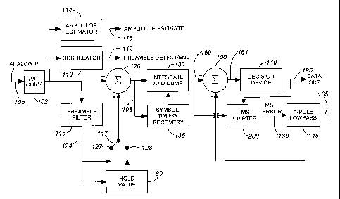
s Figure 1 is an overall schematic diagram of a DC restoration circuit in
accordance with the invention; and,
Figure 2 is a detailed schematic diagram of the LMS adapter component
200 shown in Figure 1.
Detailed Description of the Illustrated Preferred Embodiment
1 o Figure 1 of the drawings is a block diagram of the components of a
preferred embodiment of the DC restoration circuit of the present invention,
this
embodiment being operative after an FM discriminator circuit (demodulator) of
a radio receiver. In this embodiment the received information signal is a
packet
and the format of the packet comprises three portions, namely, an initial
15 preamble having a length of about 5 to 10 milliseconds and being a tone, a
synchronizing pattern following the tone and a data portion comprised of a
stream of symbols following thereafter.
As shown in Figure 1, an analog input signal 105, having been output
from an FM discriminator, is fed into an analog-to-digital (A/D) converter 102
2 o and the digital signal output from the A/D converter (referred to herein
as the
"digitized input signal") is input to each of a correlator circuit 110, which
detects
the presence and ending of the preamble tone and produces a preamble
detect/end signal 112, and a signal amplitude estimator 114 which produces a
signal 116 corresponding to an estimate of the signal amplitude. The digitized
2 s input signal is also passed through a preamble filter 115 which removes
the
tone to recover the DC component of the preamble and this DC component 124
is output from filter 115. The DC component 124 is fed to a "hold value"
component 90 which stores the value of the DC component 124. When the
preamble is detected but the end of the preamble has not yet been detected a
switch 117 is caused to be in a preamble detect position 127 whereby the DC
4
CA 02357191 2001-09-07
component 124 currently being detected (i.e. prior to the end of the preamble)
is subtracted from the input signal via adder 120. However, when the end of
the
preamble is detected the output of the "hold value" component 90 is the DC
component value occurring at the time the end of the preamble is detected and
the switch 117 is caused to be in a preamble ending position 128 whereby that
ending DC component 124 is thenceforth, for that packet, subtracted from the
input signal via adder 120.
Decoding (i.e. recovery) of the data portion of the digitized input signal
begins by the end of the preamble. This is done in a conventional manner by
1 o an integrate and dump component 130, and a symbol timing recovery
component 135 which is a phase-locked loop (PLL), into each of which a
symbol stream 108 (with the DC bias present at the preamble stage having
been removed) has been input, and a decision component 140 for evaluating
a symbol acquisition value for each of the symbols of the symbol stream. The
varying DC component of the received symbol stream is determined, and
subtracted from the output 160 of the integrate and dump component 130 (this
output being the symbol acquisition values), by a feedback LMS adaptive
circuit
200 using the outputs 150, 195 of the integrate and dump and decision
components 130, 140, resp., as shown in Figure 1. The output of the LMS
2 o adaptive circuit 200 is an LMS error signal 180 and this error signal 180
is input
to a single pole lowpass filter 145 and the resulting filtered error signal
165,
which corresponds to the varying DC component, is fed back and subtracted
from the integral output stream 160 by an adder 150. The error signal 165 is
inherently adaptive and is used as a feedback signal to adjust the integral
2 5 output stream 160 by removing therefrom the varying DC component. The
varying DC component is, therefore, not present in the output integral stream
161 which is fed into the decision component 140. Advantageously, the
resultant output data signal 195 does not include either the high DC bias
associated with the preamble or the slow varying (exponential) DC component
3 o associated with the remaining portions of the input information packet.
5
CA 02357191 2001-09-07
Figure 2 of the drawings shows the components of the LMS adaptor 200
of the DC restoration circuit of this preferred embodiment. These components,
as well as those of the symbol recovery circuitry shown in Figure 1 (other
than
the A/D converter 102), are implemented in a digital signal processor (DSP) in
s this embodiment. The decisions 195 output from the decision component 140
are input to the LMS adaptor component 200 and scaled by the amplitude
estimate signal 116 via a multiplier216. In addition, as shown by Figure 2,
the
symbol integrals 160, referred to herein as symbol acquisition values, are
input
to the LMS adaptor 200. In the LMS adaptorthe current and past two decisions
(Z-' in Figure 2 represents a one symbol delay) and the symbol acquisition
value
(integral) of the next decision are scaled by gain controllers 230, 240, 250
and
260, respectively, having gain coefficients C,, CZ, C3 and C4, resp.. This
configuration constitutes a transversal filter that estimates the two-symbol
integral output 208 of the adder 205. A second adder 210 compares the
1 s integral output 208 with the estimate formed by the sum of the outputs
235, 245,
255 and 265 of the gain controllers. The difference signal output by adder 210
is the LMS error signal 180. The LMS error signal 180 is also used by an LMS
controller (algorithm) 270 to adjust the coefficients C,, C2, C3 and C4. Due
to the
inherent high pass nature of the LMS adaptor component 200 the error signal
2 0 180 tracks the DC component of the integral stream. That is, since the
four
taps (230 - 260) of the LMS adaptive filter 200 are related to the actual
digital
signal and since there is no DC tap, the estimate signal (i.e. the sum of
tapped
signals 235, 245, 255 and 265) cannot track the DC content of the input
integrals (and this makes the adaptive filter 200 an inherently high pass
filter).
2 5 Although an "integrate and dump"-type decoder is used for the preferred
embodiment other types of decoders, such as the "sample and hold"-type could
instead be used. In the case of the former, per the foregoing, the symbol
acquisition value is an integral of the symbol and in the case of the latter
the
symbol acquisition value would be a symbol sample. In each case the value
3 o needed is a metric proportional to the symbol amplitude (i.e. whether as
integral
or sample).
6
CA 02357191 2001-09-07
The individual circuit and processing functions utilised in the foregoing
described preferred embodiment are, individually, well understood by those
skilled in the art, and it is to be understood by the reader that a variety of
other
implementations may be devised by skilled persons for substitution. Further,
it should be noted that although the circuit components described herein are
preferably implemented in software by performing digital signal processing
(DSP) operations on the data it is possible to implement one or more of these
components in hardware. Persons skilled in the field of communication design
will be readily able to apply the present invention to an appropriate
1 o implementation method for a given application.
Consequently, it is to be understood that the particular embodiment
shown and described herein by way of illustration is not intended to limit the
scope of the invention claimed by the inventor which is defined by the
appended
claims.
7