Note: Descriptions are shown in the official language in which they were submitted.
CA 02357691 2001-09-17
MULTIPLE-BEAM DIODE-
PUMPED IMAGING SYSTEM
BACKGROUND OF THE INVENTION
Field of the Invention
The present invention relates to digital printing
apparatus and methods, and more particularly to a system for
imaging of recording media such a lithographic printing
members.
Description of the Related Art
Imagining devices that utilize laser power sources
frequently deliver the output of the laser to its destination
using an optical fiber arrangement. This frees th8 designer
from the need to physically locate the lasers directly
adjacent the recording medium. For example, U.S. Patent Nos.
5,351,617 and 5,385,092 disclose the use of lasers to impress
images onto lithographic printing-plate constructions. As
described in these patents, laser output can be generated
remotely and brought to the recording blank by means of
optical fibers and focusing lens assemblies.
It is important, when focusing radiation onto many types
of recording medium, to maintain satisfactory depth-of-focus
-- that is, a tolerable deviation from perfect focus on the
recording surface. Adequate depth-of-focus is important to
construction and use of the imaging apparatus; the smaller the
working depth-of-focus, the greater will be the need for fine
mechanical adjustments and vulnerability to performance
degradation due to the alignment shifts that can accompany
normal use. Depth-of-focus is maximized by keeping output
beam divergence to a minimum.
CA 02357691 2001-09-17
-1 ~a~ -
Optical efforts to reduce beam divergence also dimish
nnwar r~ancitvaim-P a lane r,annnt alter the hriahtnacc of rhP
CA 02357691 2001-09-17
-2-
radiation it corrects; a lens can only change the optical path.
Thus, optical correction presents an inherent tradeoff between
depth-of-focus and power loss. U.S. Patent No. 5,822,345
discloses an approach that utilizes the divergent output of a
s semiconductor or diode laser to optically pump a laser crystal,
which itself emits laser radiation with substantially less beam
divergence but comparable power density; the laser crystal
converts divergent incoming radiation into a single-mode output
with higher brightness. The output of the laser crystal is
focused onto the surface of a recording medium to perform the
imaging function.
The arrangements described in the '345 patent employ a
separate crystal for each diode pumping source. This is
ordinarily necessary due to the nature of laser crystals and
25 their operation. In the absence of optical excitation,
resonant cavities formed from these optical-gain crystals are
flat-flat monoliths; when optical power is delivered~to an end
face of such a crystal, however, this and the opposed face bow
-- an effect called bulk thermal lensing. To obtain a single
so transverse mode of operation (preferably the lowest-order,
fundamental TEMoo mode), with the output divergence as close as
possible to that of a diffraction-limited source, the crystal
must be implemented in a design that accounts for bulk thermal
lensing.
This phenomenon makes it even more difficult to obtain
multiple, independent outputs from a single laser crystal.
Even if the energy of each pumping source is confined to a
discrete region on one of the crystal faces, the thermal
lensing action required for lasing in one region will
30 ordinarily affect the other regions, resulting in mutual
interference. This condition is known as ~~thermal crosstalk.~~
Accordingly, the current state of the art prescribes the use of
a separate crystal for each laser channel, resulting not only
in added cost for the crystals and their mounts, but also for
3s separate focusing assemblies.
CA 02357691 2001-09-17
-3-
In addition, the configurations described in the '617 and
'092 patents (and, somewhat more pertinently, in U.S. Patent
No. 5,764,274) contemplate permanent affixation of the diode
laser packages to the optical fiber. This is due to the need
s for efficient coupling of the laser energy into the end face of
the fiber. Components are therefore permanently joined so that
the alignment therebetween remains undisturbed during
operation. Should a diode fail, not only the diode but the
entire optical-fiber assembly must be replaced. Such a
requirement is of little consequence in the arrangements
described in the '274 patent, since the the fiber is coupled to
a focusing assembly using an SMA connector or the like, which
is conveniently removed and replaced. In arrangements having
fiber outputs that are less accessible or which require more
~s involved mounting operations, however, permanent diode
affixation at the input side of the optical fiber can prove
decidedly disadvantageous.
DESCRIPTION OF T8E INVENTION
Brief Summary of the Invention
In a first aspect, the invention confers the ability to
drive a single laser crystal with multiple pumping sources to
obtain discrete, collimated outputs without substantial thezinal
crosstalk. The meaning of the term ''substantial thermal
is crosstalk~~ as used herein must be understood~in terms of the
imaging context. Basically, it means that the action of one
pumping source will not adversely interfere with the action of
another source driving the same crystal; that is, an imaging
output emanating from one crystal region will neither defeat
so nor spuriously cause an imaging output in another region.
Exactly what constitutes an "imaging output'' also depends on
the application. In a lithography environment, an ~~imaging
output" produces an image spot on the printing plate that
alters the affinity of the plate for ink or a fluid to which
CA 02357691 2001-09-17
-4-
ink will not adhere (depending on the nature of the plate).
Thus, even if the laser output has some physical effect on the
plate, it is not an "imaging output" unless that effect
translates into lithographically functional results when the
s plate is used. As a consequence, minor thermal crosstalk that
does not rise to the level of an imaging output (or its defeat)
does not qualify as ~~substantial thermal crosstalk.~~
In accordance with this aspect of the invention, measures
are taken to confine the heat associated with thermal lensing
to specif is crystal regions, as well as to isolate these
regions thermomechanically to the highest extent possible.
Thus, in one embodiment, the anterior face of the laser crystal
(i.e., the side facing the pumping sources) is provided with a
series of parallel grooves and a pair of spaced-apart metal
is strips extending across the anterior face of the crystal
perpendicular to the grooves. The strips and grooves serve to
isolate thermomechanically the regions they define, and are
aligned with the pumping sources such that the pumping-source
outputs strike the anterior crystal face in the centers of the
regions bounded by the strips and the grooves.
This type of configuration may involve permanent mounting
of the ffibers that conduct the pumping energy to the crystal.
Accordingly, in a second aspect, the invention provides for
removable affixation of the pumping laser diodes at the input
is ends of the fibers. In one embodiment, this is accomplished
using a sapphire window and a mount that places the (input) end
face of the fiber against the window. In another embodiment,
pumping laser output is coupled into a fiber whose other end
face is butted against the anterior face of the crystal.
jo For example, a suitable arrangement includes a laser
diode; a microlens associated with the laser diode (e. g.,
permanently adhered to the diode output slit); a sapphire
window, one side of which is associated with the microlens
(e. g.. permanently adhered to the lens opposite the diode
CA 02357691 2001-09-17
- 5 -
slit); and a mount for removably receiving the optical fiber such that an end
face thereof
makes contact with the free face of the sapphire window, creating a continuous
light path
extending from the laser diode to the end face of the fiber. A suitable mount,
adapted for an
optical fiber carned in a connector comprising a threaded collar coaxially
surrounding the
fiber (e.g., a SMA connector), may include a tubular stem having exterior
threads for
receiving the collar and a bore for receiving the fiber therethrough. The
sapphire window is
positioned at the rear of the mount, and the relationship of elements within
the mount is
based on the distance the fiber protrudes into or beyond the connector --
ensuring that when
the connector is attached, the end face of the fiber will reliably make
contact with the free
face of the sapphire window.
The invention therefore provides a laser diode package facilitating removable
coupling of an optical fiber to the diode, the package comprising: a laser
diode; a microlens
associated with the laser diode; a sapphire window having first and second
sides, the first
side being associated with the microlens; and means for removably receiving
the optical
fiber such that an end face thereof makes contact with the second face of the
sapphire
window, a continuous light path extending, with the fiber thus received, from
the laser diode
to the end face of the fiber.
In a third aspect, the invention exploits the structure of a typical array of
imaging
devices to reduce imaging artifacts. This aspect of the invention pertains to
any series of
imaging outputs organized into one or more groups (each consisting, for
example, of a
multiple pumped laser crystal producing multiple outputs) and focused onto a
rotating drum.
Each time the drum rotates, each output of a group produces a column or
"swath" of image
points (in accordance with data corresponding to the image to be applied); the
distance
between adjacent swaths corresponds to the image resolution, and the outputs
are indexed by
this amount to begin their next swaths each time the drum finishes rotating.
The invention
makes use of variable indexing to disrupt the periodicity of visible artifacts
associated with a
particular output, thereby reducing their visual impact. Specifically, the
outputs of each
group of laser crystals are first indexed by the resolution distance until the
regions between
CA 02357691 2001-09-17
-6-
the adjacent output beams within each group have been fully scanned. Then,
after each
group is indexed by the much larger distance between the first and last
outputs of a group
(or, expressed with respect to a recording medium on the drum, by the axial
width of the
imaging zone spanned by the group of outputs), each group is again indexed by
the
resolution distance as before. This process is continued until all unimaged
regions between
nei~-'~'~....:~.< .<.....,~" ,..... ~,"<. ,."~~~oa
CA 02357691 2001-09-17
7_
Brief Description of the Drawinas
The foregoing discussion will be understood more readily
from the following detailed description of the invention, when
taken in conjunction with the accompanying drawings, in which:
s FIG. 1 is a plan schematic illustration of the basic
components of the invention in a representative
implementation;
FIG. 2 is an isometric view of a crystal adapted to
receive four separate inputs without substantial
to crosstalk;
FIG. 3 is a sectional view of a first structure for
removably coupling an optical fiber to a laser pumping
diode, with the fiber partially inserted into the
structure; and
~s FIG. 4 is a sectional view of a second structure for
removably coupling an optical fiber to a laser pumping
diode, with the fiber removed from the structure.
CA 02357691 2001-09-17
.8.
Detailed Description of the Preferred Embodiments
Refer first to FIG. 1, which schematically illustrates
the basic components of the invention. A recording medium 50,
such as a lithographic plate blank or other graphic-arts
s construction, is affixed to a support during the imaging
process. In the depicted implementation, that support is a
cylinder 52 around which recording medium 50 is wrapped, and
which rotates as indicated by the arrow. If desired, cylinder
52 may be straightforwardly incorporated into the design of a
to conventional lithographic press, serving as the plate cylinder
of the press. Cylinder 52 is supported in a frame and rotated
by a standard electric motor or other conventional means. The
angular position of cylinder 52 is monitored by a shaft encoder
associated with a detector 55. The optical components of the
is invention, described hereinbelow, may be mounted in a writing
head for movement on a lead screw and guide bar assembly that
traverses recording medium 50 as cylinder 52 rotates. Axial
movement of the writing head results from rotation of a stepper
motor, which turns the lead screw and indexes the writing head
after each pass over cylinder 52.
Imaging radiation, which strikes recording medium 50 so
as to effect an imagewise scan, originates with a series of
pumping laser diodes 60, four of which are representatively
designated D1, D2, D3, D4. The optical components discussed
zs below concentrate laser output onto recording medium 50 as
small features, resulting in high effective power densities. A
controller 65 operates a series of laser drivers collectively
indicated at 67 (and described more fully below) to produce
.imaging bursts when the outputs of the lasers 60 are directed
3o at appropriate points opposite recording medium 50.
Controller 65 receives data from two sources. The
angular position of cylinder 52 with respect to the laser
output is constantly monitored by detector 55, which provides
signals indicative of that position to controller 65. In
CA 02357691 2001-09-17
-9-
addition, an image data source (e. g., a computer) 70 also
provides data signals to controller 65. The image data define
points on recording medium 50 where image spots are to be
written. Controller 65, therefore, correlates the
instantaneous relative positions of the focused outputs of
lasers 60 and recording medium 50 (as reported by detector 55)
with the image data to actuate the appropriate laser drivers
at the appropriate times during scan of recording medium 50.
The driver and control circuitry required to implement this
scheme is well-known in the scanner and plotter art; suitable
designs are described in the '092 patent and in U.S. Patent
No. 5,174,205, both commonly owned with the present
application.
The output of each of the lasers 60 is conducted, by
means of an optical fiber 721, 72z, 723, 724, to an alignment
bench 75 that has a series of parallel grooves 77 for
receiving the fibers. Bench 75, which may be fabricated from
materials such as metal or silicon, is aligned with a laser
crystal to direct the outputs of lasers 60 at appropriate
points on the anterior face 80f of laser crystal 80. Because
of the construction laser crystal 80 as described below, each
laser 60 stimulates a separate output from laser crystal 80
without substantial thermal crosstalk.
It is the emissions of crystal 80 that actually reach the
recording medium 50. A first lenslet array 82 concentrates
the outputs of lasers D1-D4 onto crystal 80, and a second
lenslet array 84 concentrates the outputs from crystal 80 onto
CA 02357691 2001-09-17
-9 (a) -
a focusing lens 85. The latter lens, in turn, demagnifies the
incident beams in order to concentrate them further and draw
them closer together on the surface of recording medium 50.
The relationship between the initial pitch or spacing P
between beams from crystal 80 and their final spacing on
recording medium 50 is given by Pf = P/D, where Pf is the final
spacing and D is the demagnification ratio of lens 85. For
l fl a~ramr~l c
CA 02357691 2001-09-17
-10-
the grooves 77 of bench 75 may be spaced 400 um apart, which
also determines the pitch P. If the demagnification ratio of
lens 85 is 4:1, then the spots will be spaced 100 ~.rm apart on
the surface of recording medium 50.
s Given the characteristics of currently available laser
crystals, four pumping sources per crystal is a preferred
configuration. Different configurations are of course
possible, however. Most commercial imaging applications will
require more than four simultaneously actuable laser beams.
One may therefore employ a writing head having multiple
crystals (each receiving, for example, four pumping inputs)
focused through the same or separate optical components 82, 85
and all advanced by the same lead screw. The use of a series
of multiply pumped laser crystals is also favored in order to
is minimize imaging artifacts, as described below.
A variety of laser crystals can serve in the present
invention so long as they lase efficiently at the desired
imaging wavelength and produce a collimated output. Preferred
crystals are doped with a rare earth element, generally
zo neodymium (Nd), and include Nd:YV04, Nd:YLF and Nd:YAG
crystals. It should be understood, however, that advantageous
results may be obtainable with other laser crystals.
with reference to FIG. 2, laser crystal 80 is modified in
order to receive energy from multiple pumping sources and to
Zs provide, in response thereto, discrete outputs without
substantial thermal crosstalk. Crystal 80 has a series of
parallel longitudinal grooves 100 and transverse grooves 101
cut into end face 80f. Grooves 100, 101 may be, for example,
?-10 arm deep and spaced 100 um apart. (Typically, crystal 80
so _.~ 0.5-2.0 mm thick, with a polarization vector Vp oriented as
shown.)
A pair of metal strips 1021, 1022 extend across face 80f
of crystal 80 parallel to grooves 101; a complementary pair of
metal strips 1023, 1024 extend across the posterior face of
CA 02357691 2001-09-17
-11-
crystal 80. Metals strips 102 may be, for example, gold, 0.8
um in height and 0.005 um thick, and may be applied by vacuum
deposition or other suitable means. Their purpose is to
thermally couple the contacted regions of crystal SO to a heat
sinking arrangement (such as that disclosed in U.S. Patent No.
5, 990, 925) .
Grooves 100, 101 define a series of four bounded regions.
The outputs of the pumping lasers are desirably directed at
the centerpoints 105 of these regions. In response, crystal
80 will produce four separate outputs without substantial
thermal crosstalk.
The grouped structure of the laser diodes is
advantageously employed to minimize imaging artifacts. These
tend to occur at the boundaries between zones imaged by
adjacent imaging devices, and reflect slight imperfections in
inter-device spacings. The visual effect of these
imperfections can be reduced or eliminated by exploiting the
inter-device spacing within each array and the spacing between
arrays to permit indexing by different amounts. Variable
indexing disrupts the periodicity of imaging errors, making
them less noticeable.
Suppose, for example, that the array shown in FIG. 1 is
one of several arrays in a single writing head, that the pitch
P in each array is 400 um, and that the demagnification ratio
of lens 85 is 4:1 to produce spots spaced 100 um apart on the
surface of recording medium 50. Suppose, further, that the
desired dot resolution (i.e. the spacing between adjacent dots
on recording medium 50) is 20 ~.zm. Each time cylinder 52
CA 02357691 2001-09-17
-11 (a) -
rotates, each of the four diodes 60 produces a column or
"swath" of image points. After a rotation, the array is
S indexed by 20 um (the resolution or "spot-pitch" distance);
and after the array has been indexed four times lsc~ that frnir
CA 02357691 2001-09-17
-12-
columns spaced 20 arm apart have been applied), the entire zone
spanned by the array has been imaged. The writing head is then
indexed by 300 inn, the distance representing the width of the
imaging zone. Since the spacing between arrays ordinarily is
s substantially larger than the zone width, each array will be
indexed through multiple zone widths throughout the course of a
scan. Because of this variable indexing (i.e., at both the
resolution and zone-width distances), imaging errors will
generally be less noticeable as compared with, for example, a
system in which the devices are indexed only by the resolution
distance.
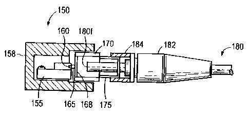
FIG. 3 illustrates a first mounting structure
facilitating removable coupling of any of laser diodes DI-D4 to
its respective fiber 721-724 (see FIG 1). The structure,
is indicated generally at 150, guides the output of a laser diode
155 into the end face of an optical ffiber without the need for
permanent affixation thereto. Mounting structure 150 includes
a housing 158 having an interior cavity for receiving the diode
package 155, Which is permanently affixed therein. Housing 158
so contains suitable openings, not shown, that facilitate
electrical connection to diode 155.
Diode 155 has an emission slit 160 through which laser
radiation is emitted. Radiation disperses as it exits slit
160, diverging at the slit edges. Generally the dispersion
~s (expressed as a 'numerical aperture," or NA) along the short or
"fast" axis is of primary concern; this dispersion is reduced
using a divergence-reduction lens 165. A preferred
configuration is a cylindrical lens; however, other optical
arrangements, such as lenses having hemispherical cross-
3e sections or which correct bath fast and slow axes, can also be
used to advantage.
Lens 165 may be bonded directly to diode 155 at slit 160.
In front of lens 165 is a sapphire window 168, which is carried
at the end of a tubular cartridge 170, forming the end face
CA 02357691 2001-09-17
-13-
thereof. Cartridge 170 is received within the interior cavity
of housing 158, and is preferably bonded therein such that the
exterior face of window 168 contacts (and may be bonded to) the
flat face of cylindrical lens 165. Cartridge 170 and housing
s 158 are preferably metal.
Cartridge I70 includes a threaded stem 175 for receiving
a fiber-optic cable 180 terminating in an SMA (or similar,
e.g., ST or FC) connector package 182, which includes a
threaded collar 184 that is free to rotate. Cable 180 emerges
within collar 184 and protrudes beyond the collar, terminating
in an end face 180_f. (The optical fiber resides within cable
180 and is indicate by the dashed line.) The length of stem
175 is chosen such that, with collar 184 fully threaded
thereover, the end face 180_f of cable 180 makes contact with
~s the interior face of sapphire window 168. Accordingly, if
diode 155 fails, its removal need not disturb the optical
cabling assembly. Instead, this is simply removed by detaching
connector 182, and the diode structure replaced.
FIG. 4 illustrates a second mounting structure
facilitating removable coupling of any of laser diodes D1-D4 to
its respective fiber 721-724 (see FIG. 1). Once again, the
illustrated structure, indicated generally at 200, guides the
output of a laser diode 155 into the end face of an optical
fiber without the need for permanent affixation thereto.
zs Mounting structure 200 includes a housing 210 having an
interior cavity for receiving the diode package 155, which is
permanently affixed therein. Housing 200 contains suitable
openings, not shown, that facilitate electrical connection to
Mode 155 .
3o The emission slit 16U of diode 155 is again directed
through a divergence-reduction lens 165, which may be a
cylindrical lens. Lens 165 is bonded to a length 215 of
optical fiber, which exits housing 210 through a ceramic sleeve
218 encased within housing 210. Projecting from housing 210
CA 02357691 2001-09-17
-14-
and concentric with sleeve 218 is a tubular stem 220 having one
or more guide slots or channels 222 therein. The fiber-optic
cable 180 terminates in a connector 225 having a rimmed or
flanged end 227 Whose diameter approximately matches the
s interior diameter of stem 220 (so as to permit connector 225 to
be conveniently received within stem 220). A pin 230 projects
radially from flange 227 and fits within guide slot 222 as
connector 225 travels axially within stem 220. The optical
fiber carried within cable 180 emerges from connector 225
through a ceramic sleeve 235, which is encased within connector
225.
The depth of guide slot 222 is chosen such that, before
pin 230 reaches the tenainus of the slot, the end face of
ceramic sleeve 235 makes mechanical contact with the end face
is of sleeve 218, thereby aligning optical fiber 215 with the
optical fiber carried within cable 180. One or both end faces
may be coated with an index-matching fluid (e. g., a cis-trans
mixture of decahydronaphthalene) to ensure proper light
transmission through the junction.
In order to ensure maintenance of mechanical contact
between the end faces of sleeves 218, 235 notwithstanding the
vibrational rigors of a commercial printing environment,
connector 225 may be provided with a spring 237, one end of
which butts against flange 227. The other end of spring 237 is
~s engaged by a mechanical member (not shown) that is urged toward
the mounting structure 200. The resulting axial force
transmitted to flange 227, the magnitude of which is determined
by the spring constant of spring 237, maintains contact between
the end faces of sleeves 218, 235. The spring constant of
3o spring 237 is chosen so as to ensure reliable contact without
damage to sleeves 218, 235 or, more likely, skew or shifting of
the end faces.
It will therefore be seen that we have developed new and
useful approaches to the design and operation of multiple-beam,
CA 02357691 2001-09-17
-15-
diode-pumped laser systems applicable to a variety of digital-
imaging environments. The terms and expressions employed
herein are used as terms of description and not of limitation,
and there is no intention, in the use of such terms and
s expressions, of excluding any equivalents of the features shown
and described or portions thereof, but it is recognized that
various modifications are possible within the scope of the
invention claimed.
to What is claimed is: