Note: Descriptions are shown in the official language in which they were submitted.
CA 02357974 2001-10-01
SEMICONDUCTOR LASER DEVICE AND
OPTICAL FIBER AMPLIFIER USING THE SAME
FIELD OF THE INVENTION
The present invention relates generally to semiconductor
laser devices of the type having an active layer (light emitting
region) with a multiple quantum well ("MQW") structure. More
particularly, this invention relates to MQW semiconductor laser
devices with higher carrier injection efficiency and enhanced
light output. The invention also relates to optical fiber
amplifiers employing the same.
BACKGROUND OF THE INVENTION
Semiconductor laser devices having an active layer (light
emitting region) employing a multiple quantum well structure are
known in the art. Such devices emit light at lower threshold
currents than semiconductor laser devices having a bulk active
layer, and have a higher optical output power.
An example of a known MQW laser device is shown in
cross-section in FIG. 1. The laser device depicted in FIG. 1
comprises a number of semiconductor layers which are formed
using known techniques on a semiconductor substrate 1, which in
the example depicted is an n-type semiconductor. The various
layers include: an n-type lower cladding layer 2A, a undoped
lower optical confinement layer 3A, an active layer 4, a undoped
upper optical confinement layer 3B, a p-type upper cladding
layer 2B, and a p-type cap layer 5. These layers are sequentially
formed on the substrate 1 by any of a number of known epitaxial
crystal growth techniques such as, for example, metal organic
chemical vapor deposition (MOCVD). An n-type lower electrode 6A
is also formed on the lower side of substrate 1 and a p-type upper
CA 02357974 2001-10-01
2
electrode is formed over cap layer 5. As depicted in FIG. 1,
active layer 4 and the adjacent optical confinement layers 3A
and 3B are formed into an elongated mesa structure using standard
photolithographic techniques. Current blocking p-type
semiconductor layer 7A and n-type semiconductor layer 7B are
then formed in the region adjacent to the mesa structure, so that,
in operation, current is injected into active layer 4 in a narrow
area.
The resulting structure is then cleaved to provide a laser
having a predetermined resonator length (L). The front facet
S1, used as a light output, is formed on one cleaved plane through
fabrication of a low reflectivity film, and the rear facet S2
is formed on the opposite facet of the cavity with a high
reflectivity film.
It is known that the active layer 4 may be designed to have
a MQW structure consisting essentially of alternate hetero-
junctions of well layers made of semiconductor material. Each
hetero- junction comprises a pair of semiconductor layers: a well
layer of a narrow band gap energy and a barrier layer. The
barrier layer has a band gap energy which is wider than that of
the well layers. Each of the various sub-layers in the MQW
structure has a thickness of several nanometers
Lower and upper optical confinement layers 3A and 3B
adjacent to active layer 4 are each designed to have a separate
confinement heterostructure (SCH), in order to enhance the
confinement of the laser light created in active layer 4, thereby
enhancing the external differential quantum efficiency of the
laser to achieve high optical output power operation.
It is also known in the art that the semiconductor laser
device of FIG. 1 may be secured in a package to form a laser module
which is suitable for use as signal light source in an optical
CA 02357974 2001-10-01
3
communications system, or as a light source for pumping an
optical fiber amplifier such as an erbium-doped fiber amplifier
(EDFA). Within the package, the laser device may be thermally
coupled to a cooling device comprising Peltier elements. The
package may also include and other known structures to monitor
and control heat generation and light output, and to ensure good
optical coupling of the laser output to an optical fiber.
In recent years, the rapid growth in the Internet and other
communications systems has led to the development of fiber-optic
wavelength division multiplexing (WDM) system architectures to
provide increased data transmission capacity in such systems.
In order to provide optical fiber amplifiers with enhanced
light output performance to meet the demand for an increased
number of channels, there has been a need for pumping lasers with
high light output coupled to the optical fiber. Pumping lasers
for optical fiber amplifiers are required to offer stable
operation with ever higher fiber-coupled light output and with
narrower spectral width, especially for use in optical fiber
Raman amplifiers.
One way to achieve a high light output pumping laser with
an MQW active layer is to increase the resonator length (L).
Increasing the resonator length decreases both the electric
resistance and thermal impedance of the laser device. This
results in a larger saturation driving current Isdr at which the
maximum optical output power occurs, since the saturation is
dominated by thermal saturation effects. However, for a given
value of output facet reflectivity, increasing L lowers causes
the external differential quantum efficiency to lower, due to
the lowering of mirror loss ratio against the total loss. Thus,
at very long cavity lengths the maximum light output tends to
CA 02357974 2001-10-01
4
saturate, due to the trade-off between the saturation driving
current and the external differential quantum efficiency.
This problem can be ameliorated to some degree by reducing
the reflectivity of the output facet. However, lowering the
reflectivity of the output facet of the laser device below a
certain value results in deterioration of the differential
quantum efficiency of the device and causes the saturation of
maximum optical output power. Reported mechanisms for such
deterioration include carrier leakage from the MQW structure to
the optical confinement and cladding layers, increased optical
absorption loss and recombination carrier loss at the
confinement layers due to the carrier leakage and non-uniform
hole injection into the MQW structure.
The graded index, separate confinement heterostructure
(GRIN-SCH) is known to be effective in suppressing deterioration
in low power short cavity lasers, where continuous GRIN or
multi-layer GRIN structure have been reported. However,for, high
power lasers, the reported results has been limited only to
two-step GRIN structures, and the results have been found to be
insufficient.
A proposed approach to attaining higher light output from
a semiconductor laser device having an MQW active layer is to
employ undoped well layers sandwiched between barrier layers
having an n- type dopant, e. g., selenium ( Se ) or sulfur ( S). This
so-called "modulation-doping" of the barrier layer suppresses
internal absorption by of the MQW structure thereby enabling
higher light output operation. However, when using MOCVD, it
is very difficult to fabricate this type of modulation-doped
structure within the active layer, because of the need for
selective doping of an n-type dopant into only the barrier layer.
For example, in cases where the n-type dopant is sulfur, the
CA 02357974 2007-10-25
72465-110
sulfur will diffuse from the barrier layers into the
adjacent well layers at the temperatures used during device
formation. Likewise, when using selenium, the well-known
memory effect causes selenium to be incorporated into the
5 well layers during the growth process. While a complete
interruption of crystal growth process can be used to
realize the intended abrupt doping profile with Se, such
interruptions can cause degradation to the interfaces
between well layers and the adjacent barrier layers,
increasing the number of nonradiative recombination centers
and, thereby, limiting the optical output of the device.
SUMMARY OF THE INVENTION
According to a first aspect, the present invention
provides a semiconductor laser comprising: an active light-
emitting layer having a multi-quantum well structure
comprising a plurality of individual semiconductor well
layers formed between adjacent semiconductor barrier layers,
at least one of said well layers and at least one of said
adjacent barrier layers being doped, and upper and lower
optical confinement layers adjacent to said active layer,
wherein said multi-quantum well structure has a cavity
length (L) greater than about 800 m and the thickness of
each of said optical confinement layers is between 20
to 50 nm.
According to another aspect, the present invention
provides a laser component incorporating the semiconductor
laser according to the first aspect of the present
invention, said laser component further comprising at least
one lens for optically coupling the output of said
semiconductor laser to a facet of an optical fiber and
CA 02357974 2007-10-25
72465-110
5a
wherein said semiconductor laser is thermally coupled to a
cooling device.
According to yet another aspect, the present
invention provides a laser component incorporating the
semiconductor laser according to the first aspect of the
present invention, said laser component further comprising
an isolator, one lens for optically coupling the output of
said semiconductor laser to a facet of an optical fiber and
wherein said semiconductor laser is thermally coupled to a
cooling device.
According to still another aspect, the present
invention provides a high optical output power semiconductor
laser comprising a semiconductor laser according to the
first aspect of the present invention, wherein: said at
least one of said well layers and said at least one adjacent
barrier layer are doped with an n-type dopant in a
concentration of about 1 x 10¹⁷ to about 3 x 1018 cm 3, each
of said optical confinement layers comprises a plurality of
sublayers, such that said sublayers have a band gap energy
which increases in step wise fashion from said active layer;
said optical confinement layers being symmetrically disposed
about said active layer; upper and lower cladding layers
formed adjacent to said upper and lower optical confinement
layers, respectively, said upper and lower cladding layers
having a band gap energy greater than the band gap energy of
said adjacent optical confinement layers; and wherein said
cavity has an antireflective coating having a reflectivity
of less than about 5% on an output facet thereof, and a
reflective coating having a reflectivity of greater than
about 90% on a rear facet thereof.
An embodiment of the present invention provides a
new and improved semiconductor laser device which avoids the
CA 02357974 2007-10-25
72465-110
5b
foregoing problems which limit high light output operation
of such a device. A laser device according to an embodiment
of the present invention is particularly useful as an
optical fiber amplifier pumping light source having high
carrier injection efficiency. Some embodiments of the
invention are able to achieve high carried injection
efficiency without increasing the unavailable currents and
are capable of enhanced light output compared to other laser
devices having an MQW structure.
An embodiment of the present invention comprises a
semiconductor laser device having a resonator length of more
than 800 um with a cladding layer disposed on an optical
confinement layer which is in contact with an MQW active
layer having multiple well layers and multiple barrier
layers, wherein an impurity is doped into at least one well
layer within the active layer and at least one barrier layer
adjacent to the well layer and wherein the thickness of the
optical confinement layer falls within a range of from 20
to 50 nm.
CA 02357974 2007-10-25
72465-110
6
Another embodiment of the present invention provides an
optical fiber amplifier pumping device comprising the above
semiconductor laser device mounted within a package containing
a cooling unit, wherein an optical fiber is coupled to the
optical output facet of the semiconductor laser device.
BRIEF DESCRIPTION OF THE DRAWINGS
FIG. 1 is a cross-sectional view of a semiconductor laser
device.
FIG. 2 is an energy band diagram showing the bad gap
energies of the MQW active layers and the adjacent optical
confinement and cladding layers in a laser structure according
to one embodiment of the present invention.
FIG. 3 is an energy band diagram showing the band gap
energies for the layers between a cladding layer and barrier
layer in accordance with an embodiment of the present invention.
FIG. 4 is a cross-sectional schematic diagram of an
exemplary laser module of the present invention.
FIG. 5 is a graph showing maximum laser optical output
power (P.,,.) as a function of the selenium doping concentration
in the active MQW layer of the present invention
FIG. 6 is a graph showing the maximum optical output power
(P.) as a function of the thickness of the optical confinement
layer in a exemplary laser device structure.
FIG. 7 is a graph showing the maximum optical output power
(Pmax) as a function of the energy difference between band gap
energy for the outermost optical confinement layer (E2) and for
the inner most optical confinement layer (E1) in an exemplary
laser structure.
FIG. 8 is a graph showing the saturation current as a
function of the energy difference between band gap energy for
CA 02357974 2001-10-01
7
the outermost optical confinement layer (E2) and for the inner
most optical confinement layer (E1) in an exemplary laser
structure.
DETAILED DESCRIPTION
In one aspect, the present invention is directed to a laser
structure (also referred to as a laser device) having the
capacity to produce a high powered optical output.
The laser device of the present invention preferably has
the layer structure depicted in the exemplary cross-sectional
schematic diagram of FIG. 1, which has been previously described.
Multiple quantum well (MQW) structure of active layer 4 of the
present invention (not depicted in FIG. 1) is sandwiched between
adjacent optical confinement layers 3A and 3B. In connection
with the desire to produce a high output laser, the present
invention is particularly useful with laser devices, of the type
depicted in FIG. 1, having a resonator cavity length (L) of 8001m
or greater.
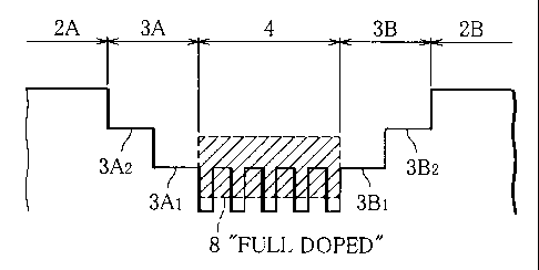
An exemplary energy band diagram of the conduction and
valence bands of a laser device of the present invention is shown
in FIG. 2. FIG. 2 shows the band gap between the conduction and
valence bands, depicting a lower optical confinement layer 3A,
an active layer 4, an upper optical confinement layer 3B and an
upper cladding layer 2B which have been formed on lower cladding
layer 2A in that order. As depicted in FIG. 2, active layer 4
comprises alternate heterojunctions of well layers 4A and
barrier layers 4B, thereby providing an MQW structure having
five wells. Optical confinement layers 3A and 3B, positioned
between active layer 4 and cladding layers 2A, 2B are preferably
formed in such a manner that their respective composition and
thickness are symmetrical about active layer 4. Each of the
CA 02357974 2001-10-01
8
optical confinement layers 3A, 3B has a plurality of steps in
their respective energy bands, as shown in FIG. 2. Thus, in the
embodiment of FIG. 2, optical confinement layer 3B has two
sublayers 3B1 and 3B2. In order to achieve the preferred
symmetrical construction of the device, optical confinement
layer 3A has two corresponding sublayers, 3A1 and 3A2.
As depicted in FIG. 2, the band gap is smallest in the wells
of the MQW structure of active layer 4, is greater at the barrier
layers in the MQW, is still greater in the optical confinement
layers, and is greatest at the cladding layers.
A first principal feature of the laser device of the present
invention is that a dopant is incorporated into at least one well
layer 4A of the active layer 4 and its adjacent barrier layer
4B to thereby form a doped region 8. Although FIG. 2 depicts
doped region 8 as having only a one barrier layer and one well,
according to the present invention doped region 8 may extend to
any number of pairs of well layers and barrier layers. Indeed,
according to the present invention the entire active layer may
be included in doped region 8. The inventors have determined
that extending the doped region to the entire active layer 4
reduces the series resistivity and thermal resistivity of the
laser device. In this manner, the device's thermal impedance
and heat generation are reduced, permitting increased maximum
light output.
The dopant used to form doped region 8 is preferably an
n-type impurity, such as 5, Se and Si (silicon) or combinations
thereof. Preferably the doping concentration is set within a
range of about from 1 x 10" to 3 x 1018 cm-3. The inventors have
found that if the doping concentration is below about 1 x 1017cm"3
then the aforementioned benefits of creating doped region 8 in
active layer 4 are not obtained, such that the intended
CA 02357974 2001-10-01
9
enhancement in light output is not realized. On the other hand,
the inventors have found that if the dopant concentration is
above about 3x1018cm-3 then the crystallinity of active layer 4
can be degraded causing non-radiative components to likewise
increase. This impairs the operation of the resulting laser
device.
Although an n-type dopant is preferred, the dopant used in
the present invention may alternatively be a p-type dopant. The
p-type impurity in such case may be any one of beryllium,
magnesium or zinc or combinations thereof.
Another important feature of the laser device of this
invention is that the two optical confinement layers 3A, 3B shown
in FIG. 2 are specifically arranged so that the thickness of each
is set to fall within a range of 20 to 50nm. If the thickness
of optical confinement layers 3B, 3A is reduced to less than 20nm
then resultant light output can reach saturation due to overflow
of electrons. On the other hand, if the thickness of optical
confinement layers 3B, 3A is increased above 50nm or greater then
the resulting DC resistance of the laser device increases. This
causes increased heat generation which, in turn, causes light
output saturation due to thermal saturation.
Optical confinement layers 3B, 3A form heterojunctions
with the respective barrier layers 4B positioned at the
outermost part of active layer 4. Similarly, the optical
confinement layers also form heterojunctions with upper and
lower cladding layers 2B and 2A. Preferably, the band gap energy
at the heterojunctions with cladding layers 2B and 2A is greater
than the band gap energy at the heterojunctions between the
outermost well layer 4A and its neighboring outermost barrier
layer 4B within active layer 4. More preferably, the difference
between the band gap energy E, of such barrier layer and the
CA 02357974 2001-10-01
maximal band gap energy E2 of optical confinement layer is about
90meV or more, as shown in FIG. 2.
As shown in FIG. 2, optical confinement layers 3A and 3B
preferably comprise two or more sublayers, for example,
5 sublayers 3B1, 3B2 and 3A1, 3A2. According to the present
invention, the band gap energies of these respective sublayers
increase in stepwise fashion as the distance from active layer
4 increases, as shown in FIGS. 2 and 3. FIG. 3 shows a series
of points, Al, A2, A0 at the edges of the steps in the band gap
10 of optical confinement layer 3B formed by the sublayers 3B1 and
3B2. Note that the point A0 is formed at the step between optical
confinement sublayer 3B2 and the adjacent cladding layer 2B.
Also depicted in FIG. 3 is the point A0' which is located at
the step in band gap energy between barrier layer 4B and the
adjacent well layer 4A. The points A0', Al, A2 and A0 define
an envelope line of the band gap energies of the layers, (this
envelope line will be referred to hereafter as band gap energy
line). Preferably, this band gap energy line is a straight or
has a continuous upward or downward convex shape as shown by
broken lines in FIG. 3. The upward or downward convex shape may
be, for example, parabolic.
Thus, in the case of FIG. 3, the band gap energy line
intersects the band gap energy of layer 3B2 at a point A2, such
that the band gap energy line has a straight line shape as a whole.
In this case, optical confinement layer 3B is said to have a
linear GRIN-SCH structure.
As previously noted, optical confinement layers 3A and 3B
are not limited only to the exemplary two-layer structure
depicted in FIGS. 2 and 3. Increasing the number of sublayers
is preferred. However, increasing the number of layers requires
careful control of composition of each layer - if even one of
CA 02357974 2001-10-01
11
them goes out of specified lattice matching conditions then
crystal degradation can occur due to crystal defects, which in
turn may degrade laser performance. Additionally, increasing
the number of sublayers results in an increase in number of
crystal growth process steps, increasing the difficulty of
mass-production. In light of these issues, it is presently
preferred that the number of sublayers be set to at about five
(5) or six (6), which are preferably arranged so that their
respective band gap energies being fall on the band gap energy
line described above.
Preferably the laser device of the present invention is
formed such that its well layer 4A has compressive strain of
between about 0.5% to about 1.5% with respect to the substrate
1.
As noted above, it is preferred that the laser device of
the present invention have resonator length (L) of about 800im
or more. More preferably, L is greater than about 1000im. When
the resonator length is less than about 800im the laser device
has greater electrical resistivity and thermal-impedance,
lowering in saturation current, (since thermal saturation
dominates the saturation current). Thus, when the resonator
length is less than about 800 Im, the benefits of the present
invention are not fully realized. When using a relatively long
resonator cavity, J. e. , resonator cavity of about 800 im or more,
it is preferable that reflectivity of the front facet of the
laser device be about 5% or less and that the reflectivity of
the rear facet be about 90% or greater. Applying a low-
reflectivity film on the front facet of the laser device
compensates for the decrease in efficiency which would otherwise
occur due to reduced ratio of mirror loss against total losses
caused by the use of an elongated resonator. This makes it
CA 02357974 2001-10-01
12
possible to suppress overflow of carriers created, thereby
overcoming the problem of reduced optical output power reduction
at high drive current when compared to prior art structures.
Next, an exemplary laser component of the present invention
is described with reference to FIG. 4. The laser component 40
has a laser device 8 sealed within a package 10. Laser device
8 is mounted on a cooling device 9 comprising a plurality of
Peltier elements 9a. A collimator lens lla is disposed adjacent
to the output facet of the laser device 8 and a light collection
or focusing lens llb is positioned near a wall of package 10.
An optical fiber 12 is positioned at the front of the package
10 adjacent to lens llb, such that the light emitted by laser
device 8 is coupled to fiber 12. A photodiode 13 is disposed
adjacent to the rear facet of the laser device 8 to monitor the
light output from the device.
Preferably, optical fiber 12 has an optical fiber grating
12b formed in its central core 12a. Preferably, the reflection
bandwidth of fiber grating 12b is set at about 3nm or less. More
preferably, the reflection bandwidth of the fiber grating is set
about 2nm or less, and even more preferably it is set at about
1.5 nm or less . However, the reflection band width of fiber
grating 12b should be greater than the wavelength separation of
the longitudinal modes in the light from the laser device 8.
Setting the grating bandwidth in this manner reduces or
eliminates kinks in the current versus light output
characteristics of laser light from the optical fiber 12, while
simultaneously narrowing the spectrum width of the light to
enable enhanced multiplexing. In the module shown in Fig.4,
present invention realizes a higher output power and more stable
operation due to broader gain bandwidth.
CA 02357974 2001-10-01
13
Exa_mnle
A plurality of semiconductor laser devices according to the
present invention having wavelength of 1480nm and the layer
structure shown in FIG. 1 were manufactured in the following
manner, and the relation of the parameters versus laser
characteristics were analyzed while changing various parameters
of the devices which were constructed.
Influence of impurity doping into active layer.
An n-type cladding layer 2A comprised of n-type InP was
fabricated on the (100) plane of a substrate 1 made of n-type
InP. A lower optical confinement layer 3A was formed on this
lower cladding layer 2A. The optical confinement layer 3A was
made of undoped InGaAsP-based semiconductor material with a
GRIN-SCH structure as follows: First, a layer 3A2 made of InGaAsP
(eg=1.1 im) having a thickness of 20im was formed; then, a layer
3A1 made of undoped InGaAsP (eg=1.2 im) was formed thereon to
a thickness of 20nm. An active layer 4, described in detail below,
was then formed on this lower optical confinement layer 3A. Next
an upper optical confinement layer 3B was formed thereon,
comprising a layer 3B1 made of undoped InGaAsP (eg=1.2 im) with
a thickness of 20nm and a layer 3B2 made of undoped InGaAsP
(eg=1.1 im) with a thickness of 20nm. Thus, the upper and lower
optical confinement layers were made to be symmetrical about the
active layer.
Active layer 4 was formed with five wells 4A made of GaInAsP
each having a thickness of 4nm. Each of the well layers was
surrounded by a barrier layer 4B made of GaInAsP with a thickness
of lOnm. The overall MQW active layer structure was formed to
have a compressive strain of 1% as a whole. An n-type dopant
Se was incorporated into the layers of the MQW active layer to
CA 02357974 2001-10-01
14
form an impurity-doped region 8 arranged as discussed below. A
first set of devices was created having doping in all of the MQW
layers (referred to as the "fully doped" herein) with a dopant
concentration of 1 x 1017cm-3 in all of the well layers 4A and
barrier layers 4B. A second set of devices was created with
doping only in a pair consisting of a centrally located well
layer 4A and an adjacent barrier layer 4B (referred to
hereinafter as "centrally doped") with a dopant concentration
of 5 x 1017cm-3. In addition, a set of devices was created having
an undoped active layer 4 as a comparative example (referred to
as "undoped" hereinafter).
Thereafter, mesa were formed on the devices using standard
photolithographic and etching techniques and a p-type current
blocking layer 7A and n-type current blocking layer 7B for
current constriction were formed in the area adjacent to the
resulting mesas. An upper cladding layer 2B made of p-type InP
was then formed on the upper optical confinement layer 3B, and
a contact layer 5 made of p-type InGaAs was formed thereon. A
p-type upper electrode 6B was then formed on contact layer 5 and
the back surface of substrate 1 was polished. An n-type
electrode 6A the formed on the resulting polished surface.
The resulting structures were then cleaved to set the
resonator length (L) at 10001m, and a low reflectivity film
(reflectivity of 1%) was formed on the front facet S1 and a high
reflectivity film (reflectivity of 95%) was formed on the rear
facet S2 to complete the fabrication of the laser devices.
With regard to the laser devices of three different types,
the maximum light output (Pmax) during current driving was
measured. Results thus obtained are shown in Table 1 below.
CA 02357974 2001-10-01
Table 1
Impurity Doped Region at Pmax (Relative
Active Layer Value)
Fully Doped 1.2
Centrally Doped 1.07
Undoped 1.0
Table 1 compares the maximum optical output power Pmax for
three types of LDs with different doping conditions and with
5 cavity length 1000 um. From Table 1 it can be seen that if all
of the well layers and barrier layers of the active layer are
doped, high light output operation is achieved.
Next, for fully doped devices, the relationship between
Pmax and the level of n-type (Se) doping concentration was
10 investigated. The laser devices used for this investigation had
the same in structure as described above, except that their
resonator length (L) was set at 1300im. The results are shown
in FIG. 5.
As shown in FIG. 5, the value of Pmax reaches a distinct
15 maxima which, for the devices investigated is about 400mW when
the Se doping concentration is set at 1 x 1018cm-3. At lower or
higher dopant concentrations, the effect of doping
comparatively decreases. Thus, according to the present
invention the value of doping concentration in the active layer
is set to maximize Pmax.
Influence of thickness of GRIN-SCH structure
Laser devices were then manufactured with the same in
structure as has been discussed previously except that the
structure of their GRIN-SCH optical confinement layers were
varied to investigate how differences in thickness affected the
CA 02357974 2001-10-01
16
laser output. As described, the upper optical confinement layer
3B and the lower optical confinement layer 3A were comprised of
a two-layer structure of having sublayers 3B1, 3B2 and 3A1, 3A2,
respectively. For this investigation, the active layers were
fully doped (Se doping concentration 1 x 1018cm-3 ).
The value of Pmax of the resulting laser devices was
measured and the results are shown in FIG. 6. Again, the data
show a fairly distinct maxima at around 400mw for an optical
confinement layer thickness of about 40nm. FIG. 6 also shows
that high optical output power operation of more than 360mW was
obtained when the thickness of the optical confinement layer was
in the range of about 20 to 50nm.
Tnfluence of band gap energy difference between the outermost
Qrti ca1 confinement layer (=y) and the inner most optical
conf inement layer ( El-L,
Fully doped laser devices were then manufactured with the
same structure previously described, but with the resonator
length (L) being set at 1300 im and with the concentration of
Se doping of the active layer being set at 5 x 1017cm-3, in order
to investigate the effect of the band gap energy difference
(E2-E1) between the outer most optical confinement layer and for
the inner most optical confinement layer. Additionally laser
devices with E2 - E1 = 0 were also manufactured.
Pmax values of these laser devices were measured and the
results are shown in FIG. 7. The optical output power versus
current characteristics of the laser devices were also analyzed
to determine the saturation output current, and the resultant
values are shown in FIG. 8, in the form of a graph of the
saturation current as a function of the value of E2 - El. FIG. 7
shows that the light output increases with an increase in the
CA 02357974 2001-10-01
17
value of E2 - E1. When the value of E2 - E1 is about 90meV or more,
light output of more than 360mW was obtained. In the devices
investigated, saturation occurred at about 400mW. FIG. 8 shows
that a laser device having an EZ- E1 of 90meV has a saturation
output current greater than about 1200 mA, thereby enabling
driving with large injection currents, which, in turn, makes it
possible to attain a high maximum light output.
Although the exemplary embodiments used laser devices of
1480 nm, it will be apparent to those skilled in the art that
the present invention is not limited to such lasers. In
particular, it will be appreciated that the devices of the
present invention will also be particularly useful with Raman
amplifying light sources of 1200 to 1550nm.
Also, although the present invention has been explained
with respect to an exemplary GaInAsP-based laser device on InP
substrate, it will be apparent to those skilled in the art that
the invention is not limited to such a structure; for example,
the invention has application to an A1GaInAsP-based laser device
on InP substrate and to AlGaInP or AlGaInNAsP or GaInAsP-based
laser devices on GaAs substrates. Furthermore, those skilled
in the art will appreciate that the substrate may be modified
to p-type substrate.
The laser device of the present invention is high in carrier
injection efficiency and also in optical confinement effect of
optical confinement layers while offering enhanced optical
output power and thus is successfully adaptable for use as a
light source for pumping optical fiber amplifiers. Accordingly,
the laser device of the present invention is particularly well
suited for use as a light source for use in advanced systems under
strict requirements of W-class optical output power performance,
CA 02357974 2001-10-01
18
such as, for example, erbium-doped optical fiber amplifiers
and/or fiber Bragg grating-coupled Raman amplifiers.
While the present invention has been described in respect
to particular embodiments thereof, those skilled in the art will
appreciate that other changes and modifications may be made
without departing from the spirit of the invention. Therefore,
the invention should be construed to be limited only by the
following claims.