Note: Descriptions are shown in the official language in which they were submitted.
CA 02358295 2001-10-04
TITLE OF THE INVENTION
EL Panel
TECHNICAL FIELD
This invention relates to an inorganic
electroluminescent (EL) panel, and more particularly, to a
full color EL panel having light emitting layers for the
three primaries RGB.
BACKGROUND OF THE INVENTION
In the recent years, active research works have been
made on thin-film EL devices as small or large-size,
lightweight flat panel displays. A monochromatic thin-film
EL display using a phosphor thin film of manganese-doped
zinc sulfide capable of emitting yellowish orange light has
already become commercially practical as a dual insulated
structure using thin-film insulating layers 2 and 4 as
shown in FIG. 2. In FIG. 2, a predetermined pattern of
lower electrodes 5 is formed on a substrate 1, and a first
insulating layer 2 is formed on the lower electrode-bearing
substrate 1. On the first insulating layer 2, a light-
emitting layer 3 and a second insulating layer 4 are
successively formed. On the second insulating layer 4, a
predetermined pattern of upper electrodes 6 is formed so as
to construct a matrix circuit with the lower electrodes 5.
Thin-film EL displays must display images in color in
order that they find use as computer, TV and similar
monitors. Thin-film EL displays using sulfide phosphor
thin films are fully reliable and resistant to environment,
but at present regarded unsuitable as color displays
because EL phosphors required to emit light in the
primaries of red, green and blue have poor characteristics.
Engineers continued research on SrS:Ce (using SrS as a
matrix material and Ce as a luminescence center) and ZnS:Tm
as a candidate for the blue light-emitting phosphor, ZnS:Sm
-1-
CA 02358295 2001-10-04
and CaS:Eu as a candidate for the red light-emitting
phosphor, and ZnS:Tb and CaS:Ce as a candidate for the
green light-emitting phosphor.
These phosphor thin films capable of emitting light
in the primaries of red, green and blue suffer from
problems of emission luminance, emission efficiency and
color purity. Thus color EL panels have not reached the
commercial stage. Referring to the blue color among
others, a relatively high luminance is achieved using
SrS:Ce. However, its luminance is still short as the blue
color for full-color display and its chromaticity is
shifted toward green. There is a desire to have a better
blue light-emitting layer.
To solve the above problem, thiogallate and
thioaluminate base blue phosphors such as SrGa2S4:Ce,
CaGa2S4 : Ce , and BaAlZS4 : Eu were developed as described in
JP-A 7-122364, JP-A 8-134440, Communication Society
Technical Report, EID 98-113, pp. 19-24, and Jpn. J. Appl.
Phys., Vol. 38 (1999), pp. L1291-1292. These thiogallate
base phosphors are satisfactory in color purity, but suffer
from a low luminance and especially, difficulty to form a
thin film of uniform composition because of the multi-
component composition. It is believed that thin films of
quality are not obtainable because of poor crystallinity
resulting from inconvenient composition control, formation
of defects resulting from sulfur removal, and admittance of
impurities; and these factors lead to a failure to increase
the luminance. In particular, thioaluminate base phosphors
are quite difficult to control their composition.
In order to develop practical full-color_EL panels.,. _
phosphor materials capable of providing blue, green and red
phosphors in a consistent manner and at a low cost are
necessary. Since matrix materials of phosphor thin films
and luminescence center materials individually have
differing chemical or physical properties as described
above, light-emitting performance differs depending on the
-2-
CA 02358295 2001-10-04
identity of the phosphor thin film. Especially, the
response speed and afterglow of light emission differ
between different luminescence centers. To drive blue,
green and red pixels, a burning method matching with each
color is necessary.
Moreover, the EL spectra of the aforementioned blue,
green and red EL phosphor thin films are all broad. When
they are used in a full-color EL panel, RGB necessary as
the panel must be cut out of the EL spectra of the EL
phosphor thin films using filters. Use of filters
complicates the manufacture process and, still worse,
brings about a lowering of luminance. When RGB is taken
out through filters, the luminance of blue, green and red
EL phosphor thin films suffers a loss of 10 to 50~ so that
the luminance is reduced below the practically acceptable
level.
To solve the above-discussed problem, there remains a
need for red, green and blue phosphor thin film materials
capable of emitting light of a sufficient color purity to
eliminate a need for filters and at a high luminance, as
well as an EL panel in which an identical luminescence
center is used in red, green and blue phosphor thin films
so that they have the same response speed and afterglow of
light emission, allowing a common drive method to be used
to drive blue, green and red pixels, without a need for a
separate burning method matching with each color.
SUMMARY OF THE INVENTION
An object of the invention is to provide an EL panel
comprising phosphor thin films eliminating a need for RGB
phosphor filters, having a satisfactory color purity and
best suited for driving RGB in full-color EL display.
This and other objects are attained by the present
invention which provides an EL panel comprising EL phosphor
thin films of three types which emit red, green and blue
light, respectively, the EL phosphor thin films of three
types commonly and essentially containing europium as a
_3_
CA 02358295 2001-10-04
luminescence center.
In one preferred embodiment, the EL phosphor thin
films of three types have the compositional formula:
AXByOZSW:R
wherein A is at least one element selected from the group
consisting of Mg, Ca, Sr, Ba and rare earth elements, B is
at least one element selected from the group consisting of
A1, Ga and In, x is in the range of 0 to 5, y is in the
range of 0 to 15, z is in the range of 0 to 30, w is in the
range of 0 to 30, and R is an element serving as the
luminescence center and essentially containing europium.
In a further preferred embodiment, the EL phosphor
thin film which emits red light is made of a matrix
material comprising an alkaline earth sulfide, the EL
phosphor thin film which emits green light is made of a
matrix material comprising an alkaline earth thiogallate,
and the EL phosphor thin film which emits blue light is
made of a matrix material comprising an alkaline earth
thioaluminate. Typically, the alkaline earth sulfide is
calcium sulfide; the alkaline earth thiogallate is
strontium thiogallate; and the alkaline earth thioaluminate
is barium thioaluminate.
In a further preferred embodiment, the EL phosphor
thin films of three types which emit red, green and blue
light, respectively, each comprise an oxysulfide obtained
by incorporating oxygen in at least one compound selected
from the group consisting of an alkaline earth sulfide,
alkaline earth thioaluminate, alkaline earth thiogallate,
and alkaline earth thioindate. The molar ratio of oxygen
element to sulfur element in the oxysulfide, as expressed
by O/(S+O), is in the range between 0.01 and 0.85.
In another embodiment, any one of the EL phosphor
thin films of three types which emit red, green and blue
light, respectively, is made of an oxide.
BRIEF DESCRIPTION OF THE DRAWINGS
-4-
CA 02358295 2001-10-04
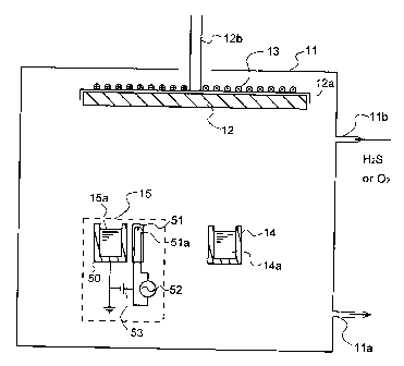
FIG. 1 is a schematic cross-sectional view showing an
exemplary construction of manufacturing apparatus to which
the invention is applicable.
FIG. 2 is a partially cross-sectional, perspective
view showing an exemplary construction of an inorganic EL
device according to the invention.
DESCRIPTION OF THE PREFERRED EMBODIMENTS
The EL panel of the invention has EL phosphor thin
films of three types which emit red, green and blue light,
respectively. The element added as a luminescence center
to the EL phosphor thin films of three types essentially
contains at least europium (Eu) commonly to the three
types.
The EL phosphor thin films of three types which emit
red, green and blue light, respectively, each are made of a
matrix material selected from among an alkaline earth
sulfide, alkaline earth oxide, alkaline earth
thioaluminate, alkaline earth aluminate, alkaline earth
thiogallate, alkaline earth gallate, alkaline earth indate,
and alkaline earth thioindate, to which at least Eu is
added as the luminescence center.
These EL phosphor thin films emit red, green and blue
light of a sufficient color purity to eliminate a need for
filters and to a high luminance. Since Eu is used as a
common luminescence center in red, green and blue phosphor
thin films so that they have the same response speed and
afterglow of light emission, the EL panel can use a common
drive method to drive blue, green and red pixels, without a
need for a separate burning method matching with each
color.
For the emissions of red, green and blue light, light
emission having a maximum wavelength in at least the
wavelength region of 600 to 700 nm is referred to as red
light, light emission having a maximum wavelength in at
least the wavelength region of 500 to 600 nm is referred to
as green light, and light emission having a maximum
-5-
CA 02358295 2001-10-04
wavelength in at least the wavelength region of 400 to 500
nm is referred to as blue light.
Examples of the alkaline earth thioaluminates,
alkaline earth aluminates, alkaline earth thiogallates,
alkaline earth gallates, alkaline earth indates, and
alkaline earth thioindates used in EL phosphor thin films
include ASBZCe , A4BZC~ , AzB2C5 , ABZC4 , AB4C7 , A4B14Czs . ABeCl3 , arid
AB12C19, etc. wherein A is an alkaline earth element, B is
aluminum (A1), gallium (Ga) or indium (In) and C is sulfur
or oxygen. The matrix material may use these compounds
alone or in admixture of two or more and take an amorphous
state where a distinct crystalline structure is absent.
The alkaline earth element is selected from Be, Mg,
Ca, Sr, Ba and Ra. Of these, Mg, Ca, Sr and Ba are
preferred, with Ba and Sr being especially preferred.
The element to be combined with the alkaline earth
element is A1, Ga or In, and any desired combination is
possible.
The phosphor thin film further contains sulfur and
oxygen in the matrix material and preferably has the
following compositional formula:
AXByOZSw:R
wherein A is at least one element selected from the group
consisting of Mg, Ca, Sr, Ba and rare earth elements; B is
at least one element selected from A1, Ga and In; and R is
an element serving as a luminescence center and essentially
containing Eu.
In the above formula, x, y, z and w denote molar
ratios of elements A, B, 0 and S, respectively, and are
preferably in the ranges of x = 0 to 5, y = 0 to 15, z = 0
to 30, and w = 0 to 30, and more preferably, x = 1 to 5, y
- 1 to 15 , z = 3 to 30 , and w = 3 to 30 .
Oxygen is contained in the alkaline earth sulfide
matrix material, preferably in such amounts that the atomic
ratio of oxygen to sulfur in the matrix material, as
expressed by O/(S+O), is in the range from 0.01 to 0.85,
-6-
CA 02358295 2001-10-04
and especially from 0.05 to 0.5. Differently stated, the
value of z/(z+w) in the formula is preferably in the range
of 0.01 to 0.85, more preferably 0.05 to 0.5, even more
preferably 0.1 to 0.4, and especially 0.2 to 0.3.
The composition of the phosphor thin film can be
ascertained by x-ray fluorescence analysis (XRF), x-ray
photoelectron spectroscopy (XPS) or the like.
Oxygen is effective for outstandingly enhancing the
electroluminescent luminance of phosphor thin films. The
light emitting device has a lifetime in that the luminance
drops with the lapse of light emitting time. The addition
of oxygen improves the lifetime performance and prevents
the luminance from dropping. The addition of oxygen to
sulfide promotes crystallization of the matrix material
during film deposition or during post treatment such as
annealing after film deposition, and permits the rare earth
element added to undertake effective transition within the
compound crystal field, producing stable light emission at
a high luminance. As compared with the matrix material of
pure sulfide, the matrix material having oxygen added
thereto is stable in air. This is presumably because the
stable oxide component protects the sulfide component in
the film from the ambient air.
In an alternative embodiment, the EL phosphor thin
films are made of oxides. The oxides have an improved
emission life and environmental resistance.
The oxides preferably have the following
compositional formula:
AXByOZ : R
wherein A is at least one element selected from the group
consisting of Mg, Ca, Sr, Ba and rare earth elements; B is
at least one element selected from Al, Ga and In; and R is
an element serving as a luminescence center and essentially
containing Eu.
[0027/28]
In the above formula, x, y and z denote molar ratios
_7_
CA 02358295 2001-10-04
of elements A, B and O, respectively, and are preferably in
the ranges of x = 0 to 5, y = 0 to 15, and z = 0 to 30, and
more preferably, x = 1 to 5, y = 1 to 15, and z = 3 to 30.
[0029/30]
Of the phosphor thin films mentioned above, the
phosphor thin film for blue light is preferably made of
BaXAlyOZSW:Eu. Oxides wherein w=0 are also preferable, with
CaXAlyOZ:Eu being especially preferred.
[0031/32]
The phosphor thin film for green light is most
preferably made of SrxGayOZSw : Eu . Oxides wherein w=0 are
also preferable , with SrXAlyOZ : Eu being especially
preferred.
The phosphor thin film for red light is preferably
made of a matrix material of alkaline earth indate having
Eu added as the luminescence center, or a matrix material
of alkaline earth sulfide having Eu added as the
luminescence center. Oxides wherein w=0 as typified by
Ga203 are also preferable .
The alkaline earth element is selected from Be, Mg,
Ca, Sr, Ba and Ra. Of these, Mg, Ca, Sr and Ba are
preferred. In the case of sulfides wherein z=0, Ca is
preferred while mixtures of two or more such as mixtures of
Ca+Sr or Ca+Mg are also acceptable. In the case of oxides
wherein w=0, Mg is preferred.
No particular limits are imposed on the thickness of
the phosphor thin film. However, too thick a film requires
an increased drive voltage whereas too thin a film results
in a low emission efficiency. Illustratively, the phosphor
thin film is preferably about 100 to 2,000 nm thick,
especially about 150 to 700 nm although the thickness
varies depending on the identity of phosphor material.
An appropriate amount of Eu added as the luminescence
center is 0.1 to 10 at% based on the alkaline earth atoms.
For CaS, an appropriate amount of Eu added is 0.1 to 0.5
at%, and most preferably 0.2 to 0.4 at%. The element added
_g_
CA 02358295 2004-05-03
as the luminescence center must contain Eu according to the
invention. Eu may be added alone or in combination with
one or more other elements. For example, the addition of
Cu or Ce to Eu as the luminescence center can improve the
response and luminance of light emission.
A red phosphor thin film may have a thickness of
about 50 to 300 nm, and preferably about 150 to 250 nm.
Too thick a film may require an increased drive voltage and
adversely affect the response, taking several seconds to
several tens of seconds until emission. Too thin a film
may result in a low emission efficiency. A film thickness.
in the above range ensures that an EL device is improved _Ln
both the response and luminance of light emission.
In a preferred embodiment, red, green and blue
phosphor thin films each have a structure of ZnS thin
film/phosphor film/ZnS thin film. As long as the phosphor
thin film is thin, the sandwiching between ZnS thin films
is effective for improving the electric charge injection
and withstand voltage of the phosphor thin film, resulting
in an EL device capable of emitting light at a high
luminance. This is true especially when CaS:Eu is used as
the phosphor thin film, providing a red EL thin film with a
high luminance and good response. The ZnS thin film may
have a thickness of about 30 to 400 nm, and preferably
about 100 to 300 nm.
In another preferred embodiment, red, green and blue:
phosphor thin films each may have a structure of ZnS thin
film/phosphor thin film/ZnS thin film, a structure of ZnS
thin film/phosphor thin film/ZnS thin film/phosphor thin
film/ZnS thin film, or a multilayer structure of ZnS thin
film/phosphor thin film/ZnS thin film/ (repeated) /phosphor
thin film/ZnS thin film.
Such phosphor thin films are preferably prepared, for
example, by the following evaporation process.
An alkaline earth sulfide having Eu added is
prepared. In a vacuum chamber, the source is evaporated by
irradiating electron beams. By~the EB evaporation of this
_g_
CA 02358295 2004-05-03
source alone or together with the evaporation of
thioaluminate, thiogallate or thioindate by resistive
heating, Eu-doped alkaline earth sulfide, alkaline earth
thiogallate, alkaline earth thioaluminate or alkaline earth
thioindate is formed. The composition is reached by
adjusting the power to the respective sources. HZS gas may
be introduced during evaporation.
Eu added to the source substance may take the form of
metal, fluoride, oxide or sulfide. Since the amount of Eu
added varies depending on the source substance and the thin
film to be deposited, the composition of the source
substance is adjusted so as to achieve an appropriate
dosage.
During the evaporation, the temperature of the
substrate may be at room temperature to 600°C, preferably
300 to 500°C. If the substrate temperature is too high,
the thin film of matrix material may have more asperities
on its surface and contain pin holes therein, giving rise
to the problem of current leakage on EL devices. Also the
thin film can be colored brown. For this reason, the
aforementioned temperature range is preferable. The film
deposition is preferably followed by annealing. The
preferred annealing temperature is 600 to 1,000°C, and more
preferably about 600 to 800°C.
The sulfide phosphor thin film thus formed is
preferably a highly crystalline thin film. Crystallinity
can be evaluated by x-ray diffraction, for example. To
promote crystallinity, the substrate temperature is set as
high as possible. It is also effective to anneal the thin
film in vacuum, N2, Ar, air, sulfur vapor or HZS after its
formation.
No particular limits are imposed on the thickness of
the light emitting layer. However, too thick a layer
requires an increased drive voltage whereas too thin a
layer results in a low emission efficiency.
-10-
CA 02358295 2001-10-04
Illustratively, the light emitting layer is preferably
about 100 to 2,000 nm thick, especially about 150 to 700 nm
although the thickness varies depending on the identity of
phosphor material.
The pressure during evaporation is preferably
1. 33x10-4 to 1.33x10⁻¹ Pa ( 1x10⁻⁶ to 1x10⁻³ Torr) . When a gas
such as HZS is introduced, the pressure may be adjusted to
6.65x10⁻³ to 6.65x10-Z Pa (5x10⁻⁵ to 5x10-' Torr). If the
pressure exceeds the range, the operation of the electron
gun becomes unstable, and composition control becomes very
difficult. The rate of gas feed is preferably 5 to 200
standard cubic centimeters per minute (SCCM), especially 10
to 30 SCCM although it varies depending on the capacity of
the vacuum system.
If desired, the substrate may be moved or rotated
during evaporation. By moving or rotating the substrate,
the deposited film becomes uniform in composition and
minimized in the variation of thickness distribution.
When the substrate is rotated, the number of
revolutions is preferably at least about 10 rpm, more
preferably about 10 to 50 rpm, and especially about 10 to
rpm. If the rotational speed of the substrate is too
high, there may arise a problem of seal upon admission into
the vacuum chamber. If the rotational speed of the
25 substrate is too low, compositional gradation may occur in
the thickness direction within the chamber so that the
resulting light emitting layer may have poor
characteristics. The means for rotating the substrate may
be any well-known rotating mechanism including a power
30 source such as a motor or hydraulic rotational mechanism
and a power transmission/gear mechanism having a
combination of gears, belts, pulleys and the like.
The means for heating the evaporation source and the
substrate may be selected, for example, from tantalum wire
heaters, sheath heaters and carbon heaters, as long as they
have the predetermined thermal capacity, reactivity or the
-11-
CA 02358295 2001-10-04
like. The temperature reached by the heating means is
preferably in the range of about 100 to about 1,400°C, and
the precision of temperature control is about ~1°C,
preferably about ~0.5°C at 1,000°C.
FIG. 1 illustrates one exemplary construction of the
apparatus for forming the light emitting layer according to
the invention. Reference is made to an embodiment wherein
Eu-doped alkaline earth sulfide, alkaline earth
thiogallate, alkaline earth thioaluminate or alkaline earth
thioindate is produced by using Eu-added alkaline earth
sulfide and any one of thiogallate, thioaluminate and
thioindate as the evaporation sources and admitting HZS
during evaporation. In the illustrated embodiment, a
substrate 12 on which the light emitting layer is to be
deposited, a resistive heating evaporation source in the
form of a Knudsen cell 14 and an EB evaporation source 15
are disposed within a vacuum chamber 11.
In the resistive heating evaporation source or K cell
14 serving as means for evaporating alkaline earth sulfide,
an alkaline earth sulfide 14a having a luminescence center
added thereto is contained. The K cell 14 is heated by a
heater (not shown) so that the metal material may evaporate
at a desired evaporation rate.
The electron beam (EB) evaporation source 15 serving
as means for evaporating thioaluminate, thiogallate or
thioindate include a crucible 50 which contains
thioaluminate, thiogallate or thioindate 15a and an
electron gun 51 having an electron emitting filament 51a
built therein. Built in the electron gun 51 is a mechanism
for controlling an electron beam. To the electron gun 51
are connected an ac power supply 52 and a bias power supply
53. The electron gun 51 produces an electron beam at a
predetermined power in a controlled manner, for evaporating
the thioaluminate, thiogallate or thioindate 15a at a
predetermined rate. Although the evaporation source is
controlled by the K cell and electron gun in the
-12-
CA 02358295 2001-10-04
illustrated embodiment, multi-source simultaneous
evaporation using a single electron gun is also possible.
The evaporation process of the latter is known as multi-
source pulse evaporation process.
In the illustrated embodiment, the evaporation
sources 14 and 15 are depicted, for the convenience of
illustration, at positions corresponding to discrete local
areas of the substrate. Actually, the evaporation sources
are located such that the deposited film may become uniform
in composition and thickness.
The vacuum chamber 11 has an exhaust port 11a through
which the chamber is evacuated to establish a predetermined
vacuum in the chamber. The vacuum chamber 11 also has an
inlet port 11b through which a reactant gas such as
hydrogen sulfide is admitted into the chamber.
The substrate 12 is fixedly secured to a holder 12a.
The holder 12a has a shaft 12b which is rotatably held by
an outside rotating shaft mount (not shown) so that the
vacuum may be maintained in the chamber 11. The shaft 12b
is adapted to be rotated at a predetermined number of
revolutions by a rotating means (not shown). A heating
means 13 in the form of a heater wire is closely secured to
the substrate holder 12a so that the substrate may be
heated and maintained at the desired temperature.
Using the illustrated apparatus, the vapor of
alkaline earth sulfide and the vapor of thioaluminate,
thiogallate or thioindate are evaporated from the K cell 14
and EB evaporation source 15 and deposited on the substrate
12 where they are bound together to form a fluorescent
layer of Eu-doped alkaline earth sulfide, alkaline earth
thiogallate, alkaline earth thioaluminate or alkaline earth
thioindate. By rotating the substrate 12 during the
evaporation process if desired, the light emitting layer
being deposited can be made more uniform in composition and
thickness distribution.
Using the phosphor thin film of the invention as a
-13-
CA 02358295 2001-10-04
light emitting layer 3, an inorganic EL device is
manufactured, for example, to the structure shown in FIG.
2.
FIG. 2 is a partially cross-sectional, perspective
view showing an exemplary construction of the inorganic EL
device using the light emitting layer of the invention. In
FIG. 2, a predetermined pattern of lower electrodes 5 is
formed on a substrate 1, and a first thick insulating layer
(or thick-film dielectric layer) 2 is formed on the lower
electrodes 5. On the first insulating layer 2, a light-
emitting layer 3 and a second insulating layer (or thin-
film dielectric layer) 4 are successively formed. On the
second insulating layer 4, a predetermined pattern of upper
electrodes 6 is formed so as to construct a matrix circuit
with the lower electrodes 5. The red, green or blue
phosphor thin film is selectively coated at the
intersections of matrix electrodes.
Between two adjacent ones of the substrate 1,
electrodes 5, 6, thick-film insulating layer 2 and thin-
film insulating layer 4, an intermediate layer such as a
bond enhancing layer, stress relief layer or reaction
preventing barrier layer may be disposed. The thick film
may be improved in smoothness as by polishing its surface
or using a smoothing layer.
Preferably, a BaTi03 thin-film layer is formed as the
barrier layer between the thick-film insulating layer and
the thin-film insulating layer.
Any desired material may used as the substrate as
long as the substrate has a heat resistant temperature or
melting point of at least 600°C, preferably at least 700°C,
especially at least 800°C so that the substrate may
withstand the thick-film forming temperature, the forming
temperature of the EL fluorescent layer and the annealing
temperature of the EL device, the substrate allows
deposition thereon of functional thin films such as a light
emitting layer by which the EL device can be constructed,
-14-
CA 02358295 2001-10-04
and the substrate maintains the predetermined strength.
Illustrative examples include glass substrates, ceramic
substrates of alumina (A1z03 ) , forsterite ( 2Mg0 ~ Si02 ) ,
steatite (Mg0 ~ Si02 ) , mullite ( 3A1203 ~ 2Si02 ) , beryllia ( Be0 ) ,
aluminum nitride (AlN), silicon nitride (SiN), and silicon
carbide (SiC+Be0) as well as heat resistant glass
substrates of crystallized glass or the like. Of these,
alumina substrates and crystallized glass substrates are
especially preferable. Where heat transfer is necessary,
beryllia, aluminum nitride, silicon carbide and the like
are preferred.
Also useful are quartz, heat oxidized silicon wafers,
etc. as well as metal substrates such as titanium,
stainless steel, Inconel and iron base materials. Where
electro-conductive substrates such as metal substrates are
used, a structure in which a thick film having an internal
electrode is formed on a substrate is preferred.
Any well-known thick-film dielectric material may be
used as the thick-film dielectric material (first
insulating layer). Materials having a relatively high
permittivity are preferred.
For example, lead titanate, lead niobate and barium
titanate based materials can be used.
The dielectric thick film has a resistivity of at
least 108 S2 ~ cm, especially about 101° to 101$ S2 ~ cm. A
material having a relatively high permittivity as well is
preferred. The permittivity E is preferably about 100 to
10,000. The preferred thickness is 5 to 50 Vim, especially
10 to 30 Vim.
The insulating layer thick film is formed by any
desired method. Methods capable of relatively easily
forming films of 10 to 50 ~m thick are useful, and the sol-
gel method and printing/firing method are especially
preferred .
Where the printing/firing method is employed, a
-15-
CA 02358295 2001-10-04
material is fractionated to an appropriate particle size
and mixed with a binder to form a paste having an
appropriate viscosity. The paste is applied onto a
substrate by a screen printing technique, and dried. The
green sheet is fired at an appropriate temperature,
yielding a thick film.
Examples of the material of which the thin-film
insulating layer (second insulating layer) is made include
silicon oxide (Si02), silicon nitride (SiN), tantalum oxide
( Taz05 ) , strontium titanate ( SrTi03 ) , yttrium oxide ( Y203 ) ,
barium titanate (BaTi03), lead titanate (PbTi03), PZT,
zirconia (Zr02), silicon oxynitride (SiON), alumina (A1203),
lead niobate, PMN-PT base materials, and multilayer or
mixed thin films of any. In forming the insulating layer
from these materials, any of conventional methods such as
evaporation, sputtering, CVD, sol-gel and printing/firing
methods may be used. The insulating layer preferably has a
thickness of about 50 to 1,000 nm, especially about 100 to
500 nm.
The electrode (lower electrode) is formed at least on
the substrate side or within the first dielectric layer.
As the electrode layer which is exposed to high temperature
during formation of a thick film and during heat treatment
along with the light emitting layer, use may be made of a
customary metal electrode containing as a main component
one or more elements selected from palladium, rhodium,
iridium, rhenium, ruthenium, platinum, tantalum, nickel,
chromium and titanium.
Another electrode layer serving as the upper
electrode is preferably a transparent electrode which is
transmissive to light in the predetermined emission
wavelength region because the emitted light often exits
from the opposite side to the substrate. When the
substrate and insulating layer are transparent, a
transparent electrode may also be used as the lower
electrode because this permits the emitted light to exit
-16-
CA 02358295 2001-10-04
from the substrate side. Use of transparent electrodes of
ZnO, ITO or the like is especially preferred. ITO
generally contains In203 and Sn0 in stoichiometry although
the oxygen content may deviate somewhat therefrom. An
appropriate proportion of Sn02 mixed with In203 is about 1
to 200, more preferably about 5 to 12o by weight. For IZO,
an appropriate proportion of Zn0 mixed with In203 is
generally about 12 to 32o by weight.
Also the electrode may be a silicon-based one. The
silicon electrode layer may be either polycrystalline
silicon (p-Si) or amorphous silicon (a-Si), or even single
crystal silicon if desired.
In addition to silicon as the main component, the
electrode is doped with an impurity for imparting electric
conductivity. Any dopant may be used as the impurity as
long as it can impart the desired conductivity. Use may be
made of dopants commonly used in the silicon semiconductor
art. Exemplary dopants are B, P, As, Sb, A1 and the like.
Of these, B, P, As, Sb and A1 are especially preferred.
The preferred dopant concentration is about 0.001 to 5 ate.
In forming the electrode layer from these materials,
any of conventional methods such as evaporation,
sputtering, CVD, sol-gel and printing/firing methods may be
used. In forming a structure in which a thick film having
an internal electrode is formed on a substrate, the same
method as used in forming the dielectric thick film is
preferred.
The electrode layer should preferably have a
resistivity of up to 1 S2~cm, especially about 0.003 to 0.1
S2~cm in order to apply an effective electric field across
the light emitting layer. The preferred thickness of the
electrode layer is about 50 to 2,000 nm, especially about
100 to 1,000 nm although it depends on the electrode
material.
The EL panel of the invention has been described
while it can be applied to other forms of display device,
-17-
CA 02358295 2001-10-04
typically full-color panels, multicolor panels and partial
color panels partially displaying three colors.
EXAMPLE
Examples are given below for illustrating the
invention in more detail.
Example 1
An EL panel according to the invention was
fabricated. For the substrate and thick-film insulating
layer, BaTi03 base dielectric material having a
permittivity of 5,000 was commonly used. For the lower
electrode, a Pd electrode was used. On fabrication, a
sheet of the substrate was formed, and the lower electrode
and thick-film insulating layer were screen printed thereon
to form a green sheet, which was co-fired. The surface was
polished, obtaining a substrate bearing a thick-film first
insulating layer of 30 ~m thick. On this substrate, a
BaTi03 coating was formed by sputtering as a buffer layer
to 400 nm. This was annealed in air at 700°C, obtaining a
composite substrate.
On the composite substrate, phosphor thin films of
three types, red, green and blue each were formed as a
structure of A1203 film ( 50 nm) /ZnS film ( 200 nm) /phosphor
thin film or light emitting layer (300 nm)/ZnS film (200
nm)/A1203 film (50 nm) in order that the resulting EL
device produce stable light emission.
To form the phosphor thin film of each color at
predetermined sites, a masking pattern was previously
furnished for each color, and each film was partially
formed by masked evaporation.
For the phosphor thin films of three types, red,
green and blue, CaS, SrGs2S4 and BaAlzS4 base phosphor thin
films were used, respectively. In every film, Eu was used
as the luminescence center.
The red phosphor thin film was prepared by the
following procedure. Used for this film formation was an
apparatus as shown in FIG. 1 wherein only one electron gun
-18-
CA 02358295 2001-10-04
was used.
An EB source 15 loaded with CaS powder having 0.5
mol% Eu added was placed in a vacuum chamber 11 into which
HZS gas was admitted. The CaS was evaporated from the
source and deposited on a rotating substrate heated at
400°C, forming a thin film. The evaporation rate of the
source was adjusted such that the film was deposited on the
substrate at a deposition rate of 1 nm/sec. The HZS gas
was fed at 20 SCCM. In this way, a phosphor thin film was
formed. Specifically the thin film was obtained as the
structure of A1203 film ( 50 nm) /ZnS film ( 200 nm) /phosphor
thin film (300 nm)/ZnS film (200 nm)/A1203 film (50 nm).
The structure was annealed in air at 750°C for 10 minutes.
Similarly, a phosphor thin film was formed on a Si
substrate. The resulting phosphor thin film in the form of
CaS:Eu thin film was analyzed for composition by
fluorescent x-ray analysis, finding an atomic ratio of
Ca:S:Eu = 24.07:25.00:0.15.
The green phosphor thin film was prepared by the
following procedure. Used for this film formation was an
apparatus as shown in FIG. 1 wherein one electron gun and
one resistive heating evaporation source (cell) were used.
An EB source 15 loaded with SrS powder having 5 mold
Eu added and a resistive heating source 14 loaded with
Ga2S3 powder were placed in a vacuum chamber 11 into which
HZS gas was admitted. The reactants were evaporated from
the respective sources and deposited on a rotating
substrate heated at 400°C, forming a thin film. The
evaporation rates of the respective sources were adjusted
such that the film was deposited on the substrate at a
deposition rate of 1 nm/sec. The HZS gas was fed at 20
SCCM. In this way, a phosphor thin film was formed.
Specifically the thin film was obtained as the structure of
A1203 film ( 50 nm) /ZnS film ( 200 nm) /phosphor thin film
( 300 nm) /ZnS film ( 200 nm) /A1203 film ( 50 nm) . The
-19-
CA 02358295 2001-10-04
structure was annealed in air at 750°C for 10 minutes.
Similarly, a phosphor thin film was formed on a Si
substrate. The resulting phosphor thin film in the form of
SrxGayOZSw:Eu thin film was analyzed for composition by
fluorescent x-ray analysis, finding an atomic ratio of
Sr:Ga:O:S:Eu = 6.02:19.00:11.63:48.99:0.34.
The blue phosphor thin film was prepared by the
following procedure. Used for this film formation was an
apparatus as shown in FIG. 1 wherein one electron gun and
one resistive heating evaporation source (cell) were used.
An EB source 15 loaded with BaS powder having 5 mold
Eu added and a resistive heating source 14 loaded with
AlzS3 powder were placed in a vacuum chamber 11 into which
HZS gas was admitted. The reactants were evaporated from
the respective sources and deposited on a rotating
substrate heated at 400°C, forming a thin film. The
evaporation rates of the respective sources were adjusted
such that the film was deposited on the substrate at a
deposition rate of 1 nm/sec. The HZS gas was fed at 20
SCCM. In this way, a phosphor thin film was formed.
Specifically the thin film was obtained as the structure of
A1203 film ( 50 nm) /ZnS film ( 200 nm) /phosphor thin film
( 300 nm) /ZnS film ( 200 nm) /A1z03 film ( 50 nm) . The
structure was annealed in air at 750°C for 10 minutes.
Similarly, a phosphor thin film was formed on a Si
substrate. The resulting phosphor thin film in the form of
BaXAlyOZSw:Eu thin film was analyzed for composition by
fluorescent x-ray analysis, finding an atomic ratio of
Ba:Al:O:S:Eu = 8.91:18.93:9.33:28.05:0.35.
By RF magnetron sputtering technique using an ITO
oxide target, a transparent ITO electrode of 200 nm thick
was formed on the resulting structure at a substrate
temperature of 250°C. The electrode was patterned to
complete an EL device of the matrix structure.
An electric field having a frequency of 240 Hz and a
-20-
CA 02358295 2001-10-04
pulse width of 50 ~S at seven different voltages was
applied to the two electrodes of each matrix in the EL
panel, providing each color with 8 bit gradation. The EL
panel emitted light in 512 colors at an average luminance
of 100 cd/m2 and with a good response.
Example 2
The procedure of Example 1 was repeated using a
SrA1Z04:Eu thin film as the green phosphor instead of the
SrXGayOZSW:Eu thin film. Substantially equivalent results
were obtained.
The EL panel of the invention employs red, green and
blue phosphor thin film materials capable of light emission
of a good color purity and high luminance without a need
for filters, and differently stated, phosphor matrix
materials having analogous chemical or physical properties
and doped with Eu as the luminescence center commonly for
all three colors. This leads to the advantages of
simplified driving of a full color EL panel, minimized
luminance variation, increased manufacturing yield, and
reduced manufacturing cost of the panel including
circuitry. The invention is of great commercial worth.
There has been described an EL panel comprising
phosphor thin films eliminating a need for RGB phosphor
filters, having a satisfactory color purity and best suited
for driving RGB in full-color EL display.
-21-