Note: Descriptions are shown in the official language in which they were submitted.
CA 02358422 2008-01-25
.1
DESCRIPTION
PAINT FOR FORMING A TRANSPARENT CONDUCTIVE THIN FILM
AND
TRANSPARENT CONDUCTIVE THIN FILM
Technical Field
The present invention relates to a paint for forming a transparent conductive
thin
film and a transparent conductive thin film. More specifically, the present
invention
relates to a paint for forming a transparent conductive thin film which is
useful as a
coating for transparent material surfaces that require the effects of blocking
static
electricity, interfering with electromagnetic waves, and the like, such as
screen surfaces
for display devices, surface covering materials of the same, window glass,
show window
glass, covering materials for instruments, material for "clean room" floors
and walls,
packaging materials for semiconductors, and the like: and a transparent
conductive thin
film obtained by means of coating the aforementioned paint as a transparent
thin film.
Background Art
In general, transparent substrates such as glass substrates used for image
display
members of CRT display apparatuses, plastic substrates for used as material
for "clean
room" floors and walls, and the like require treatment for static electricity
prevention in
order to prevent static electricity blockade. In particular, a conductive thin
film to be
treated for static electricity prevention is formed onto the surfaces of
optical parts such as
image display members of CRT display apparatuses, liquid crystal image display
members, covering materials for instruments and the like. In order to impart
the
aforementioned static electricity preventing function without losing the color
tone of
these optical parts, the aforementioned conductive thin film must comprise a
high
transparency having a total light permeability of at least 80% and a haze
value of no
CA 02358422 2001-06-26
2
greater than 5%, and a conductivity having a surface resistivity of no greater
than 9 x
101152/^
As a treatment method for static electricity prevention, a method is known in
which a transparent thin film having conductive properties is formed onto the
surface of a
transparent substrate such as glass or the like. As the material for forming
this type of
transparent conductive thin film, a paint for forming a transparent conductive
thin film is
used which comprises an antimony-doped tin oxide powder having a primary
granular
diameter of 1 - 100 nm, a binder, and a solvent.
According to this conventional method, it is possible to form a thin film
having
conductive properties stably. However, according to this conventional method,
it is
extremely difficult to form a thin film having a superior transparency with a
total light
permeability of at least 80% and a haze value of no greater than 5%. In
particular, a
transparent conductive thin film formed in accordance with the conventional
method does
not comprise a sufficient transparency, as a conductive thin film for
preventing static
electricity, when formed onto the surface of the aforementioned optical parts.
In order to solve the aforementioned problems, the present invention provides
a
paint which is effective in forming a transparent conductive thin film onto
the surface of
a transparent material, said transparent conductive thin film possessing a
superior
transparency and, moreover, a conductivity equal to or greater than that of
the
conventional transparent conductive thin film, despite the addition of only a
small
amount of the conductive component; and a transparent conductive thin film
formed by
means of using the aforementioned paint.
Disclosure of Invention
In order to solve the aforementioned problems, the present invention based on
Claim 1 provides a paint for forming a transparent conductive thin film
characterized in
comprising at least: a conductive oxide powder comprising a primary granular
diameter
of no greater than 100 nm; an easily dispersible low-boiling point solvent of
said
conductive oxide powder; a difficultly dispersible high-boiling point solvent
of said
conductive oxide powder; and a binder.
CA 02358422 2008-01-25
3
In addition, the present invention based on Claim 2 provides a paint for
forming a
transparent conductive thin film, wherein said conductive oxide powder is
selected from
among a tin oxide powder, an antimony-doped tin oxide powder, an indium oxide
powder,
and a tin-doped indium oxide powder.
Furthermore, the present invention based on Claim 3 provides a paint for
forming
a transparent conductive thin film, wherein said conductive oxide powder
comprises a
primary granular diameter of 1- 10 nm, and a secondary granular diameter of 20
- 150
nm.
In addition, the present invention based on Claim 4 provides a transparent
conductive thin film characterized in having at least one layer comprising a
transparent
conductive layer which possesses mesh-shaped openings and is formed by means
of
using said paint for forming a transparent conductive thin film.
In addition, the present invention based on Claim 5 provides a transparent
conductive thin film comprising a high transparency having a total light
permeability of
at least 80% and a haze value of no greater than 5%, and a high conductivity
having a
surface resistivity of no greater than 9 x 101152/^
The present invention relates to a paint for forming a transparent conductive
thin film
comprising; a conductive oxide powder having a primary particle diameter of no
greater than
100 nm, an easily dispersible low-boiling point solvent of the conductive
oxide powder, a
difficultly dispersible high-boiling point solvent of the conductive oxide
powder, and a
binder,
wherein the conductive oxide powder is a hydrophilic powder,
the easily dispersible low-boiling point solvent is selected from the group
consisting of water, methanol, ethanol, 2-propanol, and 1-propanol;
the difficultly dispersible high-boiling point solvent is selected from the
group
consisting of 1-ethoxy-2-propanol, 1-methoxy-2-propanol, 2-methoxyethyl
acetate, 2-
ethoxyethyl acetate, 2-butoxyethyl acetate, tetrahydrofurfuryl alcohol,
propylene
carbonate, N,N-dimethyl formamide, N-methylformamide, N-methyl pyrrolidone, 2-
ethoxy ethanol, and 2-butoxy ethanol;
a temperature difference between the easily dispersible low-boiling point
solvent and the difficultly dispersible high-boiling point solvent is 30 C or
greater;
and
a blending weight ratio of the easily dispersible low-boiling point solvent
and
the difficultly dispersible high-boiling point solvent is in a range of 95:5
to 60:40.
CA 02358422 2008-01-25
3a
The present invention relates to a paint for forming a transparent conductive
thin film
comprising: a conductive oxide powder having a primary particle diameter of no
greater than
100 nm, an easily dispersible low-boiling point solvent of the conductive
oxide powder, a
difficultly dispersible high-boiling point solvent of the conductive oxide
powder, and a
binder,
wherein the conductive oxide powder is a non-hydrophilic powder;
the easily dispersible low-boiling point solvent is selected from the group
consisting of acetone, methylethyl ketone, methylisobutyl ketone, diethyl
ketone,
tetrahydrofuran, methyl formate, ethyl formate, methyl acetate, and ethyl
acetate;
the difficultly dispersible high-boiling point solvent is selected from the
group
consisting of toluene, xylene, ethyl benzene, isophorone, cyclohexanone, 2-
ethoxy
ethanol, and 2-butoxy ethanol;
a temperature difference between the easily dispersible low-boiling point
solvent and the difficultly dispersible high-boiling point solvent is 30 C or
greater;
and
a blending weight ratio of the easily dispersible low-boiling point solvent
and
the difficultly dispersible high-boiling point solvent is in a range of 95:5
to 60:40.
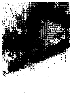
Brief Description of the Drawing
Figure 1 is a TEM photograph showing an enlargement of the transparent
conductive thin film according to the present invention.
Best Mode for Carrying Out the Invention
In the following, the present invention will be further described by means of
the
preferred embodiments. Furthermore, the preferred embodiments are for the
purpose of
more effectively explaining the present invention, and hence the present
invention is not
particularly limited thereto.
[Paint for forming a transparent conductive thin film]
The paint for forming a transparent conductive thin film according to the
present
embodiment comprises at least: a conductive oxide powder comprising a primary
granular diameter of no greater than 100 nm; an easily dispersible low-boiling
point
solvent of said conductive oxide powder; a difficultly dispersible high-
boiling point
CA 02358422 2001-06-26
4
solvent of said conductive oxide powder; and a binder dissolved in the two
aforementioned types of solvents.
Among the two or more types of solvents contained in the paint for forming a
transparent conductive thin film, the term "easily dispersible" solvent refers
to the solvent
which disperse the conductive oxide powder more easily than the other
solvent(s). On
the other hand, among the two or more types of solvents contained in the paint
for
forming a transparent conductive thin film, the term "difficultly dispersible"
solvent
refers to the solvent which disperse the conductive oxide powder more
difficultly than the
other solvent(s).
In addition, among the two or more types of solvents contained in the paint
for
forming a transparent conductive thin film, the term "low-boiling point"
solvent refers to
the solvent which has the lower boiling point than the other solvent(s). And,
among the
two or more types of solvents contained in the paint for forming a transparent
conductive
thin film, the term "high-boiling point" solvent refers to the solvent which
has the higher
boiling point than the other solvent(s). Furthermore, with regard to the "low-
boiling
point" solvent and "high-boiling point" solvent, a temperature difference of
at least 30 C
is preferred.
The conductive oxide powder is not particularly limited, as long as it
possesses
both a superior transparency and conductivity, in addition to a primary
granular diameter
of no greater than 100 nm. Appropriate examples of this conductive oxide
powder
include a tin oxide powder, an antimony-doped tin oxide (hereinafter referred
to as
"ATO") powder, an indium oxide powder, and a tin-doped indium oxide powder.
Among the aforementioned, from the perspective of transparency and
conductivity, in
particular, the ATO powder may be appropriately used.
In addition, the conductive oxide powder preferably comprises a primary
granular
diameter of 1 - 10 nm, and a secondary granular diameter of 20 - 150 nm. In
the case
when using a conductive oxide powder comprising a primary granular diameter
and
secondary granular diameter within the aforementioned ranges, a transparent
conductive
thin film having both a superior transparency and conductivity can be easily
formed.
In other words, when the primary granular diameter is less than 1 nm, the
contact
resistivity increases due to an increase in the number of contact points among
the primary
CA 02358422 2001-06-26
granules. As a result, the conductivity of the aforementioned paint decreases,
and the
granules tend to aggregate easily, such that formation of secondary granules,
in the
aforementioned paint, having diameters within the aforementioned range is not
possible.
In addition, a primary granular diameter exceeding 10 nm results in
degradation of the
transparency of the resultant conductive thin film, such that obtaining a
transparency with
a total light permeability of at least 80% and a haze value of no greater than
5% becomes
difficult.
The conductive oxide powder may also undergo various surface processing, for
example, hydrophilic processing or non-hydrophilic processing, wherein the
combination
of solvents used must be appropriately selected, as described below, depending
on the
surface treatment conditions.
The concrete examples of the "easily dispersible low-boiling point solvent of
the
conductive oxide powder" differ depending on the surface conditions of the
conductive
oxide powder to be used.
In other words, when the conductive oxide powder to be used comprises a
hydrophilic powder, examples of the easily dispersible low-boiling point
solvent of the
conductive oxide powder may include water (boiling point 100 C), methanol
(boiling
point 65 C), ethanol (boiling point 78 C), 2-propanol (boiling point 82 C), 1-
propanol
(boiling point 97 C), and the like.
In addition, when the conductive oxide powder to be used comprises a non-
hydrophilic powder, examples of the easily dispersible low-boiling point
solvent of the
conductive oxide powder may include acetone (boiling point 56 C), methylethyl
ketone
(boiling point 80 C), methylisobutyl ketone (boiling point 116 C), diethyl
ketone
(boiling point 102 C), tetrahydrofuran (boiling point 66 C), methyl formate
(boiling
point 32 C), ethyl formate (boiling point 54 C), methyl acetate (boiling point
58 C),
ethyl acetate (boiling point 77 C), and the like.
The concrete examples of the "difficultly dispersible high-boiling point
solvent of
the conductive oxide powder" also differ depending on the surface conditions
of the
conductive oxide powder to be used.
In other words, when the conductive oxide powder to be used comprises a
hydrophilic powder, examples of the difficultly dispersible high-boiling point
solvent of
CA 02358422 2001-06-26
6
the conductive oxide powder may include 1-ethoxy-2-propanol (boiling point 132
C), 1-
methoxy-2-propanol (boiling point 120 C), 2-methoxyethyl acetate (boiling
point 145 C),
2-ethoxyethyl acetate (boiling point 156 C), 2-butoxyethyl acetate (boiling
point 191 C),
tetrahydrofurfuryl alcohol (boiling point 178 C), propylene carbonate (boiling
point
242 C), N, N-dimethyl formamide (boiling point 153 C), N-methylformamide
(boiling
point 180 C), N-methyl pyrrolidone (boiling point 202 C), 2-ethoxy ethanol
(boiling
point 136 C), 2-butoxy ethanol (boiling point 170 C) and the like.
In addition, when the conductive oxide powder to be used comprises a non-
hydrophilic powder, examples of the difficultly dispersible high-boiling point
solvent of
the conductive oxide powder may include toluene (boiling point 110 C), xylene
(boiling
point 138 - 144 C), ethyl benzene (boiling point 136 C), isophorone (boiling
point
215 C), cyclohexanone (boiling point 156 C), 2-ethoxy ethanol (boiling point
136 C), 2-
butoxy ethanol (boiling point 170 C), and the like.
The aforementioned binder is not particularly limited and may comprise any
binder which is soluble in the aforementioned two or more types of solvents,
as long as a
thin film possessing a superior durability is obtainable. Examples of this
binder may
include acrylic resins such as methacrylic resins and the like, polyacetylene
resins, amino
resins such as melamine resins and the like, polyamide resins, polyimide
resins,
polyamide-imide resins, polyethylene resins, polycarbonate resins,
polyurethane resins,
polyester resins such as alkyd resins and the like, epoxy resins, polystyrene
resins, ABS
resins, polyamicsulfone resins, polyethersulfone resins, vinyl chloride
resins, vinylidene
chloride resins, vinyl acetate resins, polyvinyl alcohol resins, silicone
resins, fluorine
resins, polyphenylene oxide resins, polypyrrole resins, ultraviolet ray cure
resins,
cellulose derivatives such as diacetyl celluose, triacetyl celluose and the
like. The
aforementioned binders may be used alone or in combinations of two or more.
The blending ratios of each component in the paint for forming a transparent
conductive thin film is not particularly limited, but may comprise, for
example, 0.6 -
12% by weight of the conductive oxide powder granules, 1- 25% by weight of the
binder, with the remainder comprising at least two type of solvents.
CA 02358422 2001-06-26
7
When using a paint for forming a transparent conductive thin film having the
aforementioned blending ratios, it is possible to easily obtain a transparent
conductive
thin film comprising a surface resistivity of no greater than 9 x 101152/^, a
total light
permeability of at least 80%, and a haze value of no greater than 5%. In
particular, in the
case when ATO powder is used as the conductive oxide powder, it is possible to
easily
obtain a transparent conductive thin film comprising a surface resistivity of
1 x 10⁶ _ 9 x
101152/^, a total light permeability of at least 85%, and a haze value of no
greater than
0.5%.
In addition, among the two or more types of solvents, the blending ratio of
the
"easily dispersible low-boiling point solvent of said conductive oxide powder"
and
"difficultly dispersible high-boiling point solvent of said conductive oxide
powder"
comprises a weight ratio of 95:5 ~ 60:40. This weight ratio allows for the
easy formation
of a conductive oxide powder, within the aforementioned paint, comprising
secondary
granules having a granular diameter of 20 - 150 nm, and results in a superior
conductivity and tranparency, in addition to a superior paint dispersion
stability and easy
coating properties.
In addition, the paint for forming a transparent conductive thin film
according to
the present embodiment may be prepared from a conductive oxide powder, an
easily
dispersible low-boiling point solvent of said conductive oxide powder, a
difficultly
dispersible high-boiling point solvent of said conductive oxide powder, and a
binder, in
addition to adding and mixing in, as necessary, additives such as a dispersing
agent,
viscosity controlling agent, surface improving agent, and the like according
to the
appropriate conventional method.
At the same time, it is also possible to appropriately add a third solvent in
addition
to the easily dispersible low-boiling point solvent of said conductive oxide
powder, and
difficultly dispersible high-boiling point solvent of said conductive oxide
powder.
[Transparent Conductive Thin Film]
A transparent conductive thin film having mesh-shaped openings is obtained by
means of coating the aforementioned paint for forming a transparent conductive
thin film
CA 02358422 2001-06-26
8
onto a substrate surface such as glass, plastic or the like, and then drying,
curing, and
forming a thin film onto the substrate surface.
Here, any conventional method may be used to coat the paint for forming a
transparent conductive thin film onto the surface of the substrate: for
example, spin
coating, dip coating, spray coating, flow coating, bar coating, gravure
coating, or the like
may be used. The drying temperature is not in particular limited, as long as
the
temperature allows for the evaporation of the solvents used.
It is not always clear why a transparent conductive thin film having both a
superior transparency and conductivity is formed using the paint for forming a
transparent conductive thin film, however, a hypothesis for the aforementioned
is
described below. In other words, when the film coat formed using the paint for
forming a
transparent conductive thin film is dried, the easily dispersible low-boiling
point solvent
of said conductive oxide powder is evaporated off, which in turn results in
the gentle
aggregation of the conductive oxide powder into a mesh form. This aggregate,
while
maintaining the aforementioned mesh structure, is then solidified onto the
substrate via
the binder with the evaporation of the difficultly dispersible high-boiling
point solvent of
said conductive oxide powder to form the transparent conductive thin film
having mesh-
shaped openings, as shown in Figure 1 (TEM photograph, 500,000x enlargement).
As a result, despite adding only a small amount of the conductive component,
it is
possible to form an excellent conductive pass, and moreover, achieve an
excellent
transparency by means of the mesh-shaped openings.
Examples
In the following, the present invention will be further described by means of
the
Examples.
(Experimental Example)
As the conductive oxide powder, 0.01 g of an ATO powder (non-hydrophilic,
manufactured by Sumitomo Osaka Cement, Inc.) comprising a primary granular
diameter
of 3 - 8 nm, was respectively dispersed into 5.0 g of methylethyl ketone,
diacetone
alcohol, cyclohexanone, and toluene as the solvents. The secondary granular
diameters
CA 02358422 2001-06-26
9
of the ATO powder in these dispersed solvents were then measured using a laser
diffraction method, and the dispersibility of the ATO powder was evaluated.
These
results are shown in Table 1.
(Example 1)
0.20 g of the ATO powder used in the Experimental Example above, 17.00 g of
methylethyl ketone, 2.00 g of cyclohexanone and 0.80 g of a polyester resin
(brand name
Eliter, manufactured by Yunichika, K.K.) were mixed together as the conductive
oxide
powder, easily dispersible low-boiling point solvent of said ATO powder,
difficultly
dispersible high-boiling point solvent of said ATO powder, and binder,
respectively. The
mixture was then dispersed using an ultrasound dispersing device to yield a
paint for
forming a transparent conductive thin film of Example 1.
The secondary granular diameters of the ATO powder within the transparent
conductive paint were then measured using a laser diffraction method (PHOTON
CORRELATOR LPA-3000 manufactured by Otsuka Electron, Inc.). These results are
shown in Table 2.
The paint for forming the transparent conductive thin film of Example 1 was
then
coated onto a polyethylene terephthalate film at room temperature using a bar
coater (#7),
and dried for 10 minutes under a temperature of 100 C to form the transparent
conductive thin film.
Subsequently, the total light permeability, haze value, and surface
resistivity of
the resultant transparent conductive thin film were each measured by the
following
methods and devices. These results are shown in Table 2.
Total light permeability: HAZE METER MODEL TC-H3DPK manufactured by
Tokyo Denshoku, K.K.
Haze value: Same as above
Surface resistivity: Loresta IP manufactured by Mitsubishi Chemicals, Inc.
In addition, the film structure of this transparent conductive thin film was
observed under an electron microscope to verify the formation of a plurality
of mesh-
shaped openings.
CA 02358422 2001-06-26
(Example 2)
A paint for forming the transparent conductive thin film of Example 2 was
prepared in the same manner as Example 1, with the exception of the blending
amounts
of the ATO powder, methylethyl ketone, cyclohexanone and binder, which were
2.4 g,
12.00 g, 2.00 g, and 3.60 g, respectively.
The secondary granular diameters of the ATO powder within the transparent
conductive paint were then measured in the same manner as in Example 1. These
results
are shown in Table 2.
In the same manner as in Example 1, a transparent conductive thin film was
then
formed from the above paint for forming the transparent conductive thin film
of Example
2. Subsequently, the total light permeability, haze value, and surface
resistivity of the
resultant transparent conductive thin film were each measured in the same
manner as in
Example 1. These results are shown in Table 2.
In addition, the film structure of this transparent conductive thin film was
observed under an electron microscope to verify the formation of a plurality
of mesh-
shaped openings.
(Example 3)
A paint for forming the transparent conductive thin film of Example 3 was
prepared in the same manner as Example 1, with the exception of the blending
amounts
of methylethyl ketone and cyclohexanone which were 13.00 g and 6.00 g,
respectively.
The secondary granular diameters of the ATO powder within the transparent
conductive paint were then measured in the same manner as in Example 1. These
results
are shown in Table 2.
In the same manner as in Example 1, a transparent conductive thin film was
then
formed from the above paint for forming the transparent conductive thin film
of Example
3. Subsequently, the total light permeability, haze value, and surface
resistivity of the
resultant transparent conductive thin film were each measured in the same
manner as in
Example 1. These results are shown in Table 2.
CA 02358422 2001-06-26
11
In addition, the film structure of this transparent conductive thin film was
observed under an electron microscope to verify the formation of a plurality
of mesh-
shaped openings.
(Comparative Example 1)
The paint for forming the transparent conductive thin film of Comparative
Example 1 was prepared in the same manner as Example 1, with the exception
that only
19.00 g of methylethyl ketone was used as the solvent.
The secondary granular diameters of the ATO powder within the transparent
conductive paint were then measured in the same manner as in Example 1. These
results
are shown in Table 2.
In the same manner as in Example 1, a transparent conductive thin film was
then
formed from the above paint for forming the transparent conductive thin film
of
Comparative Example 1. Subsequently, the total light permeability, haze value,
and
surface resistivity of the resultant transparent conductive thin film were
each measured in
the same manner as in Example 1. These results are shown in Table 2.
In addition, upon viewing the film structure of this transparent conductive
thin
film under an electron microscope, there was no formation of any mesh-shaped
openings.
(Comparative Example 2)
An attempt was made to prepare the paint for forming the transparent
conductive
thin film of Comparative Example 2 in the same manner as Example 1, with the
exception that only 19.00 g of cyclohexanone was used as the solvent. However,
precipitates of ATO aggregates formed, such that coating was not possible.
CA 02358422 2001-06-26
12
Table 1
Solvent Name Boiling point ( C) Secondary granular ATO dispersibility
diameter (nm)
Methylethyl ketone 79.64 51 Excellent
Diacetone alcohol 168.10 40 Excellent
Cyclohexanone 155.65 - Poor (precipitation)
Toluene 110.63 - Poor (precipitation)
Table 2
Secondary
granular diameter Total light Haze value (%) Surface resistivity
(nm) permeability (%) (Q/ )
Example 1 113 95.3 0.2 2.7 x 10¹⁰
6.5 x 10¹⁰
Example 2 133 87.1 0.4 3.8 x 10⁸ -
5.7 x 10⁸
Example 3 130 92.8 0.3 1.1 x 10¹⁰ -
3.3 x 10¹⁰
Comparative 98 95.5 0.2 8.8 x 10¹²
Example 1 22 x 1012
Comparative - - - -
Example 2
Note: In Examples 1 - 3, due to the inclusion of a binder in the paint, the
secondary granular diameters
were larger than the secondary granular diameters of the Experimental Example.
CA 02358422 2001-06-26
13
Industrial Applicability
According to the paint for forming a transparent conductive thin film based on
Clam 1, which is characterized in comprising at least a conductive oxide
powder
comprising a primary granular diameter of no greater than 100 nm, an easily
dispersible
low-boiling point solvent of said conductive oxide powder, a difficultly
dispersible high-
boiling point solvent of said conductive oxide powder, and a binder, it is
possible to
obtain a paint for forming a transparent conductive thin film by means of
which a
transparent conductive thin film possessing a superior conductivity and
transparency may
be formed despite the addition of only a small amount of the conductive
component.
According to the paint for forming a transparent conductive thin film based on
Clam 2, wherein said conductive oxide powder is selected from among a tin
oxide
powder, an antimony-doped tin oxide powder, an indium oxide powder, and a tin-
doped
indium oxide powder, it is possible to impart both a superior transparency and
conductivity.
According to the paint for forming a transparent conductive thin film based on
Clam 3, it is possible to impart both a superior transparency and conductivity
since the
conductive oxide powder comprises a primary granular diameter of 1 - 10 nm,
and a
secondary granular diameter of 20 - 150 nm.
In addition, according to the transparent conductive thin film based on Clam
4, by
means of incorporating at least one layer comprising a transparent conductive
layer which
possesses mesh-shaped openings and is formed by means of using said paint for
forming
a transparent conductive thin film based on Clam 1, it is possible to form an
excellent
conductive pass despite the addition of only a small amount of the conductive
component,
and obtain an excellent transparency from the mesh-shaped openings.
In this manner, by means of coating, drying and curing the paint for forming a
transparent conductive thin film based on Clam 1 onto the surface of a
substrate, such as
glass, plastic or the like, it is possible to form a superior transparent
conductive thin film
comprising a plurality of mesh-shaped openings, which has transparency of a
total light
permeability of at least 80% and a haze value of no greater than 5%, and a
surface
resistivity of no greater than 9 x 101152/El.
CA 02358422 2001-06-26
14
Consequently, it is possible to form a transparent conductive thin film which
is
useful as a coating for transparent material surfaces that require the effects
of blocking
static electricity, interfering with electromagnetic waves, and the like, such
as screen
surfaces for display devices, surface covering materials of the same, window
glass, show
window glass, covering materials for instruments, material for "clean room"
floors and
walls, packaging materials for semiconductors, and the like, and thus also
broaden the
spectrum of use for such transparent conductive thin films.
The transparent conductive thin film based on Claim 5 comprises a total light
permeability of at least 80%, a haze value of no greater than 5%, and a
surface resistivity
of no greater than 9 x 101152/^, and as a result, it is possible to obtain a
film having both
a high conductivity and a high transparency.
Furthermore, the present invention has been described by means of the Claims,
but is in no manner limited to just the contents of the present description.
In addition, the
present invention also includes modifications and changes based on the Claims
of the
present invention.