Note: Descriptions are shown in the official language in which they were submitted.
CA 02359048 2001-05-29
WO 01/24066 PCT/US00/02890
A REGIONALLY TIME MULTIPLEXED EMULATION SYSTEM
BACKGROUND OF THE INVENTION
Field of the Invention
The present invention relates to the field of emulation systems. More
specifically,
the present invention relates to methodology for increasing capacity of an
emulation
system.
2. Background Information
Emulation systems for emulating circuit designs are known in the art.
Typically,
prior art emulation systems are formed using conventional general purpose
field
programmable gate arrays (FPGAs) and general purpose routing chips. A circuit
design to
be emulated is "realized" on the emulation system by compiling a "formal"
description of
the circuit design, and mapping the circuit design onto the logic elements
(LEs) of the
FPGAs and the routing chips.
As circuit designs have become larger and larger, up to and including designs
having millions of transistors, a similar increase in size of emulation
systems has become
necessary in order to emulate such circuit designs. Large emulation systems
typically
include a significant number of FPGAs as well as a significant number of
routing chips to
route signals between the FPGAs. However, given the large number of FPGAs
which may
be included in an emulation system, the number of routing chips required to
provide
adequate flexibility to concurrently route large numbers of input and output
signals to and
from an FPGA has become prohibitively expensive.
An article by Jonathan Babb et al. entitled "Logic Emulation with Virtual
Wires"
(hereinafter "Babb et al.") provides one solution to this problem, referred to
as "time
-1-
CA 02359048 2001-05-29
WO 01/24066 PCT/US00/02890
multiplexing" or the use of "virtual wires". Using time multiplexing, multiple
logical
outputs of an FPGA share a single physical output with only one of the logical
outputs
being able to output a signal on the single physical output in any given clock
cycle. Thus,
the logical outputs are multiplexed on the single physical output over time.
Similarly, a
physical input to an FPGA is shared by multiple logical inputs with only one
of the logical
inputs being able to receive an input signal on the physical input in any
given clock cycle.
All of the FPGAs in the Babb et al. system, as well as any routing chips
interconnecting
the FPGAs, are clocked by the same clock signal (see, Babb et al., p. 5, ~
2.1).
One problem with the Babb et al. system is that it is primarily designed to
emulate
synchronous logic providing synchronous signals, and does not support time
multiplexing
of asynchronous signals for emulating asynchronous logic. Rather, such
asynchronous
signals must be hard-wired to dedicated FPGA physical inputs and outputs,
while the
interconnection of time multiplexed synchronous signals is automatically
configured for
the user (see, Babb et al., p. 5, ~ 2.1).
Additionally, even with the use of time multiplexing, or in systems where
asynchronous signals are hard-wired to dedicated inputs and outputs, other
problems still
exist. One such problem is that of synchronizing clock signals in the
emulation system.
Despite the use of time multiplexing to reduce overall system size, the system
can still
remain relatively large. Such systems can range in size up to a few meters
square.
Synchronizing high frequency clock signals across such a large area creates a
significant
problem.
Thus, it is desirable to have an emulation system with improved capacity
without
the disadvantages of conventional time multiplexing. As will be described in
more detail
below, the present invention provides for an emulation system that achieves
these and
other desired results, which will be apparent to those skilled in the art from
the description
to follow.
-2-
CA 02359048 2001-05-29
WO 01/24066 PCT/US00/02890
SUMMARY OF THE INVENTION
A regionally time multiplexed emulation system is described herein. The
emulator
includes a plurality of reconfigurable logic devices with buffered I/O pins
and
reconfigurable logic elements. The reconfigurable logic devices are
reconfigurable to
emulate a circuit design using at least one user clock to clock the logic
elements and at
least one signal routing clock to time multiplex the routing of emulation
signals between
the reconfigurable logic devices, with the at least one signal routing clock
being
independent of the at least one user clock. As a result, both asynchronous as
well as
synchronous signals may be automatically routed by the mapping software of the
emulation system.
-3-
CA 02359048 2001-05-29
WO 01/24066 PCT/US00/02890
BRIEF DESCRIPTION OF DRAWINGS
The present invention will be described by way of exemplary embodiments, but
not
limitations, illustrated in the accompanying drawings in which like references
denote
similar elements, and in which:
Figure 1 is a block diagram showing an exemplary emulation system which
incorporates the teachings of the present invention;
Figure 2 is a block diagram showing an exemplary reconfigurable logic device
which may be used with one embodiment of the present invention;
Figure 3 is a block diagram showing an inter-LE crossbar network according to
one embodiment of the present invention;
Figure 4 is a block diagram of a circuit board which can be used in an
emulator
according to one embodiment of the present invention;
Figure 5 is a block diagram illustrating the concept of regional time
multiplexing
according to one embodiment of the present invention;
Figure 6 is a block diagram showing one embodiment of a mufti-clocked routing
chip suitable for use with one embodiment of the present invention;
Figures 7a and 7b are block diagrams illustrating shift registers which may be
used
to support the regional time multiplexing according to one embodiment of the
present
mvenhon.
Figure 8 is a block diagram showing a logical view of an inter-reconfigurable
logic
device crossbar network according to one embodiment of the present invention;
Figure 9 is a block diagram of a backplane assembly according to one
embodiment
of the present invention;
Figure 10 is a block diagram illustrating a logical view of an inter-board
crossbar
network according to one embodiment of the present invention; and
Figure 11 is a block diagram illustrating the concurrent bi-directional data
transfer
over a single connection according to one embodiment of the present invention.
-4-
CA 02359048 2001-05-29
WO 01/24066 PCT/US00/02890
DETAILED DESCRIPTION
In the following description, for purposes of explanation, specific numbers,
materials
and configurations are set forth in order to provide a thorough understanding
of the present
invention. However, it will be apparent to one skilled in the art that the
present invention
may be practiced without the specific details. In other instances, well known
features are
omitted or simplified in order not to obscure the present invention.
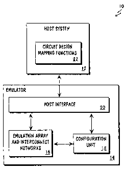
Figure 1 is a block diagram showing an exemplary emulation system which
incorporates the teachings of the present invention. As illustrated, an
emulation system 10
includes host system 12 and emulator 14. Host system 12 includes in particular
circuit
design mapping functions 22 incorporated with the teachings of the present
invention. In
one embodiment, circuit design mapping functions 22 are implemented in
software. In this
embodiment, circuit design mapping software 22 is stored in a suitable storage
medium
(not shown) of host system 12, and is loaded into memory (not shown) of host
system 12
for execution by a processor (not shown) of host system 12. Except for circuit
design
mapping functions 22, host system 12 is intended to represent a broad category
of host
systems found in conventional emulation systems known in the art, and thus
will not be
otherwise discussed further.
Emulator 14 includes emulation array and interconnect networks 16 incorporated
with the teachings of the present invention, a configuration unit 18 and host
interface 20
coupled to each other as shown. Except for emulation array and interconnecting
network
16, emulator 14 is intended to represent a broad category of elements found in
conventional emulators, whose functions and constitutions are well known to
those skilled
in the art, and therefore will not be otherwise further described either. As
will be described
in more detail below, emulation array and interconnect networks 16 comprises a
number of
reconfigurable logic elements (LEs) distributively packaged in a number of
reconfigurable
circuits and interconnected in a regional time multiplexing manner.
-5-
CA 02359048 2002-07-30
wo oinao6s rc°r~rsooroaa9o
A particular example of an emulation array and interconnect networks I6
(suitable
for incorporating the present invention) is disclosed in U.S. Patent No.
5,574,388 to
Barbier et al. The manner in which regional time multiplexing is incorporated
into
emulation array and interconnect networks 16 will be described in more detail
below.
Figure 2 is a block diagram showing one embodiment of a reconfigurable logic
device which may be used with one embodiment of the present invention. The
embodiment is of a custom or special purpose field programmable gate array
(FPGA) type,
hereinafter simply FPGA. For the purpose of this application, the term "FPGA"
is to mean
all reconfigurable circuits, and not just the typical general purpose FPGAs
available in the
market. FPGA 100 includes LE array 102, and buffered I/O pins l I3. LE array
102
includes multiple reconfigurable LEs clocked by user clocks) 118. As is well
known in
the art, the reconfigurable LEs are used to "realize" various logic elements
of circuit
designs, whereas, buffered I/O pins 113 are used to provide time multiplexed
inputs/outputs to/from FPGA 100. Each of buffered I/O pins 113 can be
statically
configured to be either an input or an output pin. This static configuration
can be
accomplished in any of a wide variety of conventional manners, such as by way
of a
configuration register.
More importantly, as illustrated in Figure 2, each of buffered I/O pins 113 is
an
inputloutput for multiple different logical inputs/outputs. In the illustrated
embodiment,
for ease of explanation, each buffered I/O pin 113 is an input/output for two
different
logical inputs/outputs, however, in alternate embodiments each buffered I/O
pin 113 is an
input/output for three or more different logical inputs/outputs. The logical
inputs/outputs
correspond to inputs to/outputs from inter-FPGA crossbar network stage
0114a/114b.
These logical inputs/outputs are time multiplexed on buffered UO pins 113 by
I/O circuitry
115, which includes a two-to-one multiplexer, and I/O circuitry 116, which
includes a one-
to-two demultiplexer, using signal routing clock 117. As illustrated, only 32
buffered I/O
-6-
CA 02359048 2002-07-30
WO 01/24066 PCT/US00/02890
pins 113 are necessary to support the 64 logical inputs/outputs due to the two-
to-one
multiplexing performed by I/O circuitry 115 and 116.
As illustrated in Figure 2, I/O circuitry 115 and 116 are clocked by signal
routing
clocks 117 whereas the LEs are clocked by a different clock signal (or
signals), user
clocks) I 18. Except for the relationship that each of signal routing clock
117 having a
higher frequency than an associated user clock 118, signal routing clocks 117
are
independent of user clocks 118. For the purpose of this application the
"associated" user
clock of a signal routing clock is the user clock employed to clock the logic
elements from
which the I/O signals of the I/O pins clocked by the signal routing clock
originate or
destined for.
In the illustrated embodiment of Figure 2, each signal routing clock 117 is of
a
higher frequency than the "associated" user clock 118, thereby allowing
signals to be
output from FPGA 100 more frequently than they are changed internally in FPGA
100.
Thus, signals can be advantageously transferred into and out of FPGA 100
asynchronously
to the changing of the signals internal to FPGA 100. Typically, the frequency
of the clock
signals) in the signal routing time domain is 10 to 100 times greater than the
frequency of
the clock signals) in the user time domain. However, different embodiments may
have
different frequency ratios.
One embodiment of I/O circuitry 115 and 116 of each of the buffered I/O pins
113
is clocked by the same signal routing clock 117. In alternate embodiments, I/O
circuitry
1 i S and 116 for different buffered I/O pins 113 can be clocked by different
signal routing
clocks rather than a single signal routing clock.
Preferably, FPGA 100 also includes memory 112, context bus 106, scan register
108, and trigger circuitry 110. Memory 112 facilitates usage of FPGA 100 to
emulate
circuit design with memory elements. Context bus 106, scan register 108 and
trigger
circuitry 110 provide on-chip integrated debugging facility for FPGA 100.
These elements
are described in U.S. Patent No. 5,777,489 to Barbier et al., entitled "Field
CA 02359048 2002-07-30
WO 41/24066 PCTIUSOO/OZ890
Programmable Gate Array with Integrated Debugging Facilities".
Inter-LE crossbar network 104 is also integrated into FPGA 100. Inter-LE
crossbar
network 104 interconnects the LEs of LE array 102, memory 112, and buffered
I/O pins
113 of FPGA 100, to be described more fully below.
Additionally, according to one embodiment, a corresponding portion of inter-
FPGA
crossbar network stage 0114a/114b is also advantageously integrated into FPGA
100.
The various portions of inter-FPGA crossbar network stage 0114a/114b together
with the
remainder of inter-FPGA crossbar network interconnect FPGAs 100 of a logic
board and
the I/0 connections of the logic board, which will also be described in more
detail below.
In one embodiment, LE array 102 includes 128 reconfigurable LEs, while memory
112 uses 8-bit input and 8-bit output, and FPGA 100 has 32 buffered I/O pins
113.
Figure 3 is a block diagram showing an inter-LE crossbar network according to
one embodiment of the present invention. For the illustrated embodiment, inter-
LE
crossbar network I04 includes four subnetworks of crossbars 400. A crossbar
device is an
interconnect device which receives multiple inputs and maps the inputs to
multiple outputs
of the device. Each input can be mapped to any of the multiple outputs. Which
inputs are
mapped to which outputs are identified by programming the crossbar device.
Such
crossbar devices are well known to those skilled in the art and thus will not
be described
further except as they pertain to the present invention.
For the illustrated embodiment, the first two subnetworks 400 are used to map
72
inputs to 160 outputs, whereas the second two subnetwork 400 are used to map
64 inputs
to 160 outputs. Each subnetwork 400 comprises three stages, stage 0, stage 1,
and stage 2.
Stage 0 of the first two subnetworks 400 include nine 8x8 crossbars 420,
whereas stage 0
of the last two of subnetworks 400 include eight 8x8 crossbars 420. In turn,
stage 1 of the
first two subnetworks 400 include eight 9x20 crossbars 440, whereas stage 1 of
the last two
subnetworks 400 include eight 8x20 crossbars 440. Stage 2 of all four
subnetworks 400
include twenty 8x8 crossbars 460.
_g_
CA 02359048 2001-05-29
WO 01/24066 PCT/US00/02890
Having now described the FPGAs including the manner in which their LEs are
interconnected on-chip and to the FPGA I/O pins, we now proceed to describe
how the
FPGAs are interconnected together on a logic board and to the logic board's
I/O pins.
Figure 4 is a block diagram of a circuit board which can be used in an
emulator
according to one embodiment of the present invention. A circuit board 600 is
shown
comprising multiple FPGAs 610 and multi-clocked routing chips (RCs) 620
coupled to
each other in a "butterfly" manner as shown. In one implementation, each of
the FPGAs
610 is an FPGA 100 of Figure 2. Each multi-clocked RC 620 includes a crossbar
622 and
related circuitry for supporting regional time multiplexing.
Recall from the earlier description that inter-FPGA network stage 0 is
distributively
implemented on FPGAs 610. Collectively, RCs 620 implement inter-FPGA network
stage
1. Together, the two stages interconnect FPGAs 610 on circuit board 600 and to
the I/O
pins 640 of circuit board 600. (As will be discussed in more detail below,
inter-FPGA
network stage 1 also "doubles up" as inter-board network stage 0.)
Thus, signals output by any of the FPGAs 610 can be routed to any other FPGA
610 on circuit board 600 or routed off board, either case, through multi-
clocked RCs 620.
Similarly, input signals to circuit board 600 can be routed to any one of the
on-board
FPGAs 610 or rerouted off board. Each of the multi-clocked RCs 620 can
advantageously
operate in multiple different signal routing time domains, with one set of at
least one I/O
pin being clocked according to one signal routing time domain while another
set of at least
one I/O pin is clocked according to another signal routing time domain. Thus,
the signals
which are transferred into and out of multi-clocked RCs 620 are time
multiplexed and
different time domains can be distributed throughout different regions of the
emulator.
This regional time multiplexing is discussed in more detail below.
In the embodiment shown, board 600 includes twenty-four FPGAs 610 and sixteen
RCs 620. However, it is to be appreciated that alternate embodiments can
include different
numbers of FPGAs and RCs.
-9-
CA 02359048 2001-05-29
WO 01/24066 PCT/US00/02890
Figure 5 is a block diagram illustrating the concept of regional time
multiplexing
according to one embodiment of the present invention. Two FPGAs 501 and 503
and a
mufti-clocked RC 502 are illustrated. In the illustrated embodiment, FPGAs 501
and 503
are both FPGAs 100 of Figure 2, and can be situated on the same or different
boards 600
of Figure 4. It is to be appreciated that, depending on their locations within
the emulator,
additional mufti-clocked RCs 502 may be needed to route signals between FPGAs
501 and
503. For ease of illustration, the internal circuitry of FPGAs 501 and 503 are
shown as
blocks 505 and 507, and are intended to represent the reconfigurable logic
elements, inter-
logic element crossbar network and inter-FPGA crossbar network stage 0, as
well as other
internal circuitry, of the FPGAs as illustrated in Figure 2.
As illustrated, the internal circuitry of FPGA 501 is clocked in a user time
domain
by clock signal 508 (clkl), whereas the I/O circuitry 515 for the input/output
of signals is
clocked in a signal routing time domain by clock signal 509 (clk2). As
discussed above,
except for clock signal 509 (clk2) being of a higher frequency than clock
signal 508, clock
signals 508 and 509 (clk2) are independent of one another.
The output signals from the internal circuitry 505 of FPGA 501 are input to
two-to-
one multiplexers of I/O circuitry 515 and output from FPGA 501 via pins 518.
Input
signals to RC 502 are received on I/O pins 521 and provided to I/O circuitry
524 where the
signals are demultiplexed and input to static routing circuitry 506 of RC 502.
The outputs
of static routing circuitry 506 are provided to I/O circuitry 527. Each of I/O
circuitry 527
also includes a two-to-one multiplexer, providing an output signal to one of
the I/O pins
530. The output signals are routed to I/O pins 533 of FPGA 503, and then
demultiplexed
by demultiplexers of I/O circuitry 536 and input to internal circuitry 507 of
FPGA 503.
In the illustrated embodiment, static routing circuitry 506 of Figure S is a
crossbar
622 of Figure 4. Static routing circuitry 506 is configured to route
particular inputs to
particular outputs as part of the programming process of the emulator. Given
the static
nature of circuitry 506, the circuitry 506 is not clocked.
-10-
CA 02359048 2001-05-29
WO 01/24066 PCT/US00/02890
As illustrated in Figure S, internal circuitry 505 of FPGA 501 is clocked in a
user
time domain by clock signal 508 (clkl), multiplexers 515 and demultiplexers
524 are
clocked in a signal routing time domain by clock signal 509 (clk2),
multiplexers 527 and
demultiplexers 536 are clocked in another signal routing time domain by clock
signal 510
(clk3), and internal circuitry 507 of FPGA 503 is clocked in another user time
domain by
clock signal 511 (clk4).
Thus, two user time domains and two signal routing time domains are
illustrated in
Figure 5, as clocked by clock signals 508, 509, 510, and 511. As illustrated,
different sets
of I/O pins and related I/O circuitry of RC 502 are clocked by different clock
signals.
Thus, signals can be advantageously transferred out of RC 502 asynchronously
to the input
of signals to RC 502 by outputting the signals from a different set than the
signals were
input on.
In an alternate embodiment of the present invention, user clock signals 508
and 511 are the
same clock signal. Thus, in this alternate embodiment, internal circuitry 505
and 507 are
both in the same time domain.
In alternate embodiments of the present invention, multiple RCs are used to
interconnect two FPGAs. Thus, in the embodiment illustrated in Figure 5,
additional RCs
could replace RC 502. Each of these additional RCs could be clocked in the
signal routing
time domains of clock signals 509 or 510, or according to additional signal
routing time
domains) (not shown).
Thus, Figure 5 illustrates regional time multiplexing in which two different
signal
routing time domains are distributed throughout the emulator. As illustrated,
different
regions of the emulator are clocked according to different signal routing time
domain clock
signals. It is to be appreciated that additional signal routing time domains
(not shown) can
also be distributed throughout the emulator.
In an alternate embodiment of the present invention, signals are routed
directly
from I/O pins 510 of FPGA 501 to/from I/O pins 533 of FPGA 503 without being
routed
through RC 502. I/O circuitry 515 and 536 are both clocked by one of either
signal routing
-11-
CA 02359048 2001-05-29
WO 01/24066 PCT/US00/02890
clock 509 or signal routing clock 510. Thus, even though a routing chip is not
used in this
alternate embodiment, the signal routing between FPGAs is still clocked by a
signal
independent of the user clock signal(s).
In another alternate embodiment of the present invention, signal routing clock
509
and signal routing clock 510 are the same clock signal. Thus, although all
inputs/outputs
of the RC 502 are clocked by the same signal routing clock signal in this
alternate
embodiment, the signal routing clock 510 is still independent of the user
clocks 508 and
511. Thus, information can still be input to/output from FPGAs asynchronously
to the
changing of signals within the internal circuitry of the FPGAs.
Figure 6 is a block diagram showing one embodiment of a mufti-clocked RC 620
suitable for use in circuit board 600 in more detail. For ease of explanation,
only two I/O
pins 633 and 634 and associated circuitry are illustrated in Figure 6. It is
to be appreciated
that the remaining I/O pins of RC 620 have similar associated circuitry. I/O
pin 633 is
enabled as either an input or an output by driver 660 and driver 665. Driver
660 is enabled
if I/O pin 633 is to be an input, and driver 665 is enabled if I/O pin 633 is
to be an output.
When operating as an input, signals received on pin 633 are provided to
latches 655, which
latch in the value on pin 633 on the falling edge of clock signal 509. These
latched signals
will be input to the interconnect 675 by drivers 670. The enablement of driver
660 or
driver 665 is performed as part of the programming of the emulator.
Outputs from RC 620 via I/O pin 633 are controlled by latches 685 and switch
690.
Outputs from interconnect 675 are provided to latches 685 via drivers 680.
Latches 685
are clocked by clock signal 509 and latch in a value from their respective
drivers 680 on
the rising edge of clock signal 509. The outputs of latches 685 are provided
to switch 690,
which is also controlled by the rising edge of clock signal 509. The latched
value from one
of the latches 685 is output by switch 690, as controlled by clock signal 509.
Similarly, I/O pin 634 is enabled as either an input or an output by driver
661 and
driver 667. Driver 661 is enabled if I/O pin 634 is to be an input, and driver
667 is enabled
if I/O pin 634 is to be an output. When operating as an input, signals
received on pin 634
-12-
CA 02359048 2001-05-29
WO 01/24066 PCT/US00/02890
are provided to latches 656, which latch in the value on pin 634 on the
falling edge of clock
signal 510. These latched signals will be input to the interconnect 675 by
drivers 671.
Outputs from RC 620 via I/O pin 634 are controlled by latches 686 and switch
691.
Outputs from interconnect 675 are provided to latches 686 via drivers 681.
Latches 686
are clocked by clock signal 510 and latch in a value from their respective
drivers 681 on
the rising edge of clock signal 510 The outputs of latches 686 are provided to
switch 691,
which is also controlled by the rising edge of clock signal 510. The latched
value from one
of the latches 686 is output by switch 691, as controlled by clock signal 510.
In the embodiment illustrated in Figure 6, driver 670, driver 680 and
interconnect
675 are referred to as the "static" part of RC 620, denoted by dashed box 676.
The static
part of RC 620 does not operate based on clock signals, so signals can be
sampled out of
the static part without regard for the clock frequency at which they were
sampled in.
Similarly, latches 655 and 685, drivers 660 and 665, and switch 690 are
referred to as the
"dynamic" part of RC 620.
Thus, as illustrated in Figure 6, two different inputs/outputs of RC 620 are
operating in two different signal routing time domains, clocked by two
different clock
signals. This separation advantageously allows time domains to be changed by
simply
routing through an RC 620. In other words, a signal can be input to RC 620 via
I/O pin
633 in the time domain clocked by clock signal 509, and output from RC 620 via
I/O pin
634 in the time domain clocked by clock signal 510.
In an alternate embodiment of the present invention, the latches 685 and 686
are not
included, and the output of drivers 680 and 681 are input directly to switches
690 and 691,
respectively. In this alternate embodiment, an additional latch (not shown),
clocked by
clock signal 509, is situated between switch 690 and driver 665, and another
latch (not
shown), clocked by clock signal 510, is situated between switch 690 and driver
667.
According to one embodiment of the present invention, RC 620 is clocked by two
different signal routing clock signals, and the I/O pins are grouped in
different sets, with
each set being clocked in a different signal routing time domain. According to
one
-13-
CA 02359048 2001-05-29
WO 01/24066 PCT/US00/02890
implementation, the I/O pins on one side of RC 620 are part of a first set
while the I/O pins
on the other side of RC 620 are part of a second set.
According to alternate embodiments of the present invention, additional sets
of I/O
pins of RC 620 are clocked according to additional clock signals. A set of I/O
pins can
include a number of pins ranging from one to (x-1 ) where x is equal to the
total number of
I/O pins on RC 620. Each of these different sets is clocked in a different
time domain. An
RC 620 can support up to x different signal routing time domains at any one
time.
In the illustrated embodiment, multiplexers and demultiplexers are used to
support
the regional time multiplexing of the present invention. Alternate embodiments
of the
present invention can utilize any of a wide variety of conventional mechanisms
for sharing
of a single physical signal by multiple logical signals. Figures 7a and 7b
illustrate one
such alternate embodiment.
Figure 7a is a block diagram illustrating an output register which may be used
to
support the regional time multiplexing according to one embodiment of the
present
invention. A parallel input, serial output shift register 720 is illustrated
including four
register cells 721, 722, 723, and 724. Inputs to register 720 are from
internal circuitry 711,
712, 713, and 714 through latches 715a-715d. Internal circuitry 711, 712, 713,
and 714
can be any of a wide range of circuitry. Internal circuitry 711, 712, 713, and
714 and
latches 715a-715d are clocked by internal clock signal 717, and register 720
is clocked by
time multiplexing clock signal 718. Data is input to cells 721, 722, 723, and
724 in
parallel, then shifted out serially as serial output 725 starting with cell
724. Thus, four
logical internal signals, received from internal circuitry 711, 712, 713, and
714, are output
via a single output signal 725. In the illustrated embodiment, clock signal
718 has a
frequency four times that of clock signal 717. Thus, every clock signal 717
cycle a new set
of four data signals can be transferred to register 720, with one signal being
shifted out of
register 720 every clock signal 718 cycle.
Figure 7b is a block diagram illustrating an input register which may be used
to
support the regional time multiplexing according to one embodiment of the
present
-14-
CA 02359048 2001-05-29
WO 01/24066 PCT/US00/02890
invention. A serial input, parallel output shift register 730 is illustrated
including four cells
731, 732, 733, and 734. Inputs to shift register 730 are shifted in serially
from serial input
735, with input data shifting from cell 734 up to cell 731. In the illustrated
embodiment,
clock signal 738 has a frequency four times that of clock signal 737. Thus,
every clock
signal 737 cycle a new set of four data signals can be transferred from
register 730 to
internal circuitry 741, 742, 743, and 744 through latches 745a-745d. Internal
circuitry
741, 742, 743, and 744 can be any of a wide range of circuitry.
Figure 8 is a block diagram showing a logical view of an inter-FPGA crossbar
network according to one embodiment of the present invention. As described
earlier, the
inter-FPGA crossbar network 750 interconnects the FPGAs on a circuit board
such that
signals can be routed between any of the FPGAs on the circuit board. In
addition, the
inter-FPGA crossbar network 750 also interconnects the FPGAs to the circuit
board I/O
connections so that signals can be routed between the circuit board I/O
connections and the
FPGAs. The interconnection of logical signals is illustrated in Figure 8. As
discussed
above, the actual physical transfer of these signals is performed using the
regional time
multiplexing of the present invention.
The routing of signals in the inter-FPGA crossbar network 750 spans both the
FPGA level and the circuit board level. A division line 700 is shown in Figure
8 which
identifies a separation between FPGA level 701 and board level 702. Crossbars
230
(corresponding to stage 114a/114b) is implemented in FPGA 610 of Figure 4. The
second
stage of the inter-FPGA crossbar network, however, is implemented in the board
level 702.
I/O signals (16) from each of the four crossbars 230 of the 24 FPGAs (4x24 =
96) are
coupled to the "FPGA-side" of the 16 RCs 631. On the "board-side" of 16 RCs
631, 28 x
16 = 448 signals are coupled to and from the logic board's I/O connections
640:
Multiple signal routing time domains are also illustrated in Figure 8. The
outputs
of the FPGAs, from crossbars 230, are in signal routing time domains) 703. As
discussed
above, different sets of I/Os from an FPGA, or different FPGAs, can be in
different signal
routing time domains. Similarly, the RCs 631 are in signal routing time
domains) 704.
-15-
CA 02359048 2001-05-29
WO 01/24066 PCT/US00/02890
As discussed above, different sets of I/Os from an RC, or different RCs, can
be in different
signal routing time domains.
For the above described embodiment, wherein there are 24 FPGAs 610, each
having 64 I/O connections, disposed on circuit board 600, having 448 I/O
connections, a
total of {(24 x 64) + 448} or {1536 + 448} are interconnected together by
inter-FPGA
crossbar network 750.
Figure 9 is a block diagram of a backplane assembly according to one
embodiment
of the present invention. Backplane assembly 800 is used to interconnect
circuit boards
820. Circuit boards 820 may be logic boards 600 of Figure 4 or I/O boards for
interfacing
with external devices. In other words, backplane assembly 800 is used to
interconnect
FPGAs disposed on logic boards 600 with each other and with external devices.
Backplane assembly 800 comprises backplane 810 and a number of matrix boards
835.
Backplane 810 is used to accept circuit boards 820, whereas matrix boards 835
are used to
interconnect signals to and from the various circuit boards 820.
Recall from earlier descriptions that inter-FPGA crossbar network stage 1 also
"doubles up" as inter-board crossbar network stage 0. Collectively, the 16
sets of 28 RCs
805 implement inter-board crossbar network stage 1. Together, the two stages
implement
the inter-board crossbar network. As discussed above, different sets of I/Os
of the RCs 620
and 837 can be in different time domains. Additionally, each of the crossbar
1010
inputs/outputs can be configured with the regional time multiplexing circuitry
of the
present invention.
Figure 10 is a block diagram illustrating a logical view of an inter-board
crossbar
network according to one embodiment of the present invention. As described
earlier, inter-
board crossbar network 905 spans two physical form levels, i.e. board level
702 and
backplane level 902 separated by dotted line 900. As shown, for the
illustrated
embodiment, stage 0 comprises 23 124x124 crossbars 631, each having 28 board
I/O
connections, whereas stage 1 comprises 28 27x27 crossbars 940, each having 23
"board-
side" I/O connections. The 28 board I/O connections of the 23 crossbars 631
and the 23
-16-
CA 02359048 2001-05-29
WO 01/24066 PCT/US00/02890
"board-side" I/O connections of the 28 crossbars 940 are connected to each
other in a
"butterfly" manner. Additionally, each crossbar 940 also has 4 "crate-side"
I/O
connections. The interconnection of logical signals is illustrated in Figure
10. As
discussed above, the actual physical transfer of these signals is performed
using the
regional time multiplexing of the present invention.
Signals are transferred between two chips of the emulator described above via
physical connections between those chips. According to one embodiment of the
present
invention, each of the physical connections allows for concurrent bi-
directional data
transfer. Figure 1l is a block diagram illustrating the concurrent bi-
directional data
transfer over a single connection according to one embodiment of the present
invention.
As illustrated, two chips 1102 and 1104 are connected via a connection 1108.
Connection
1108 is intended to represent a wide range of conventional connection media,
including
both wires and circuit board traces. According to one embodiment of the
present
invention, the FPGAs and RCs discussed above are connected together
analogously to
chips 1102 and 1104. For ease of explanation, only a single connection between
two chips
is illustrated. It is to be appreciated that additional signals can also be
transferred between
the chips in an analogous manner.
Chips 1102 and 1104 can simultaneously transfer signals to each other via
connection 1108. Chips 1102 and 1104 each include I/O circuitry, including a
driver and a
detection logic as illustrated. An output signal 1121 to be output by chip
1102 is driven
onto connection 1108 via driver 1122. Concurrently, an output signal 1132 to
be output by
chip 1104 is driven onto connection 1108 via driver 1133. After the signals
are driven onto
connection 1108, detection logics 1125 and 1135 each sample the voltage level
of
connection 1108. Based on the sampled voltage level of connection 1108, as
well as
possibly the output signal 1132, detection logic 1135 provides an input signal
1131 to the
internal circuitry of chip 1104 which is representative of output signal 1121
driven by chip
1102. Similarly, based on the sampled voltage level of connection 1108, as
well as
possibly the output signal 1121, detection logic 1125 provides an input signal
1122 to the
-17-
CA 02359048 2001-05-29
WO 01/24066 PCT/US00/02890
internal circuitry of chip 1102 which is representative of output signal 1132
driven by chip
1104.
As is well-known to those skilled in the art, driving a particular value onto
a
connection is done by asserting a particular voltage level on the connection.
A value of a
logical zero is typically in the range of 0.0 volts to 0.5 volts, and the
value of a logical one
is typically in the range of 1.8 volts to 2.4 volts. Detection logics 1125 and
1135 use these
voltage ranges in part to determine the value being driven by the other chip
according to
the following procedure. If the voltage level of connection 1108 is less than
0.5 volts, then
both chips were driving a logical zero. If the voltage level of connection
1108 is greater
than 1.8 volts, then both chips were driving a logical one. However, if the
voltage level is
between 0.5 volts and 1.8 volts, then one of the chips was driving a logical
zero while the
other was driving a logical one. As illustrated, detection logics 1125 and
1135 both receive
as inputs the output signals being driven by their respective chips. According
to the
present invention, detection logic 1125 can, in the situation of a voltage
level on
connection 1108 between 0.5 volts and 1.8 volts, conclude that the signal
output by chip
1104 is the inverse of the signal being output by chip 1102. Similarly,
detection logic 1135
can, in the situation of a voltage level on connection 1108 between 0.5 volts
and 1.8 volts,
conclude that the signal output by chip 1102 is the inverse of the signal
being output by
chip 1104.
Thus, a single physical connection between two chips can be used to
simultaneously transfer signals bi-directionally between those chips.
In the discussions above the regional time multiplexing is described as using
two-
to-one multiplexing, with two logical connections corresponding to one
physical
connection. Alternate embodiments of the present invention can use different
numbers of
inputs and outputs for the multiplexing, with m physical connections
corresponding to n
logical connections, where n > m, using an n to m multiplexer.
-18-
CA 02359048 2001-05-29
WO 01/24066 PCT/US00/02890
In the discussion above, the emulator is described as including multiple
FPGAs. In
alternate embodiments, other reconfigurable logic devices are used in the
emulator rather
than FPGAs.
Also in the discussions above, reference is made to chips which include pins.
It is
to be appreciated that the present invention can also be practiced in
embodiments where
chips do not include pins, such as where chips are surface mounted to circuit
boards.
Thus, by separating the emulator into different regions, each being a separate
time
domain, asynchronous logic may be emulated without hard-wiring asynchronous
signals to
dedicated pins. Additionally, the problem of synchronizing clock signals is
advantageously reduced, regardless of the overall size of the emulator. By not
requiring
the same clock signal to be routed throughout the entire system, the clock
signals in the
emulator no longer need to be synchronized across such a large area.
While the emulation system of the present invention has been described in
terms of
the above illustrated embodiments, those skilled in the art will recognize
that the invention
is not limited to the embodiments described. The present invention can be
practiced with
modification and alteration within the spirit and scope of the appended
claims. The
description is thus to be regarded as illustrative instead of restrictive on
the present
invention.
-19-