Note: Descriptions are shown in the official language in which they were submitted.
CA 02359225 2008-01-18
METHOD AND DEVICE FOR VIBRATION CONTROL
Background of the Invention
In the competitive marketplace which exists for automated surface-mount (SMT)
electronics equipment, including systems for fabricating electronics equipment
or components,
improvements in accuracy and speed are a significant advantage. Such equipment
is often used
in fabricating, for example, semiconductor chips, printed circuit boards,
liquid crystal displays,
and thin film devices, and may feature multiple gantry/head assemblies, linear
motors,
photoimaging systems, etching systems, and/or a number of other technologies.
The present
invention relates to devices and methods for reducing vibration inherent in
such equipment
during operation thereby to improve the speed and/or accuracy of such
equipment.
For example, modern photolithography tools require extremely high exposure
accuracy.
This can only be achieved if the levels of elastic displacement at crucial
points in the tool do not
exceed several nano-meters. Since lithography tools contain numerous moving
parts such as the
reticle and wafer stages, they are subject to persistent disturbing forces
acting on their structure.
Moreover, the tool structure is subject to environmental disturbances such as
floor vibrations and
air turbulence. While the level of these disturbances can be reduced, they
cannot be eliminated in
their entirety.
There are a number of existing techniques employed to limit the elastic
vibration of
lithography tools. For example, the stiffness of the structure that supports
key elements such as
the lens assembly may be increased, tuned mass dampers may be used, the
signals applied to the
moving stages may be shaped, or the floor vibrations may be isolated using
actively controlled
CA 02359225 2001-07-27
WO 00/45067 PCTIUSOO/02251
-2-
air springs. While effective in reducing elastic vibration, these methods
often'do not meet the
stringent requirements of more advanced photolithography tools.
Current efforts to control vibration on SMT placement equipment include
placing
frictional damping device at the end of the gantry. This "friction block"
serves mainly to
stabilize the gantry and head trajectory control system, but it also has been
shown to reduce the
settling time during certain pick and place operations. However, the
effectiveness of the friction
block depends on precise tuning of the normal force (or pre-load). The
friction block tends to
wear out quickly, greatly reducing its effectiveness and contaminating the
rest of the machine
with particles. Moreover, the friction block works against rigid body
movement, resulting in
slower operation of the equipment. The vibration control system of the present
invention, which
comprises an actuator assembly, serves to replace the friction block entirely
while improving
settling time, or, alternatively, to operate in conjunction with the friction
block, providing
additional accuracy or speed of operation.
One aspect of the present invention relates to actuator elements useful for
active vibration
reduction, structural control, dynamic testing, precision positioning, motion
sensing and control,
and active damping. Electroactive materials, such as piezoelectric,
electrostrictive or
magnetostrictive materials, are useful in such tasks. In one embodiment of the
invention, bare
electroactive elements are used. In another embodiment, packaged electroactive
elements, as
described herein, are used.
Thus, improvements are desirable in the manner in which vibration is
controlled in
systems for fabricating electronic components, as well as the manner in which
an actuator is
attached to the equipment to be controlled.
Summary of the Invention
In one embodiment of the invention, a vibration control system is provided
comprising an
actuator assembly, and a sensor for sensing a parameter of movement or
performance. The
vibration control system is particularly useful for controlling vibration in
systems for fabricating
electronics components, which often include one or more gantry assemblies,
head assemblies,
and/or moving stages or components. Contemplated systems for fabricating
electronics
components include, but are not limited to, pick and place systems,
lithography systems, and
CA 02359225 2001-07-27
WO 00/45067 PCT/US00/02251
-3-
those used to fabricate semiconductor chips, printed circuit boards, liquid
crystal displays, and
thin film devices. However, the devices and methods of the invention would be
useful in
fabricating systems of any sort, such as machine tool equipment, milling
equipment, or systems
used in an automated assembly line. Also contemplated are systems for
fabricating electronic
components wherein the systems comprise a lens system, a wafer stage, and a
structure for
supporting the lens system and wafer stage where the lens system creates an
image on the wafer
stage such as would be used in modern photolithography.
In one embodiment, an active vibration control system for use with a
photolithography
fabricating system includes the following components: a sensor that measures
the displacement
levels at the key points, or provides information from which such information
can be estimated; a
digital or analog processor that can compute a control signal based on the
sensors input, and an
actuator that can induce elastic displacement in the structure.
In a particularly preferred embodiment, an actuator useful in an active
vibration control
system used in conjunction with photolithography tools is non-reactive and
does not require back
support (actuators that require back support may excite elastic vibrations in
the support structure,
which may be re-introduced unto the tool), and has a very low distortion
profile (an actuator
array designed to control structural vibration at a given frequency or band
must not excite any
vibration outside that band).
In a particularly preferred embodiment, a vibration control system in
accordance with the
invention comprises an induced-strain actuator that acts directly on the
strain state of the
structure, and has virtually no distortion. Such an actuator can excite, and
therefore control, only
the elastic vibration modes of the controlled structure, leaving all other
vibration modes (such as
the modes of various equipment housing structures, etc.) uncontrolled. This
contributes to the
control system simplicity and robustness.
In another preferred embodiment of the invention, the vibration control system
further
comprises a circuit in electrical communication with the actuator assembly and
the sensor. In
one embodiment, the sensor relays information about movement, vibration or
performance to the
circuit, which, in response, signals the actuator assembly to control
vibration. The vibration in
CA 02359225 2001-07-27
WO 00/45067 PCTIUSOO/02251
-4-
the systems in which the present invention are useful may be due to external
disturbance or due
to the inherent disturbances generated by the system itself.
In yet another preferred embodiment of the invention, the vibration control
system further
comprises an electrical connection to the fabricating system. The electrical
connection may
provide for the fabricating system to send to, or receive from the vibration
control system
information such as abling or disabling signals, system status signals, or
fault/error status signals.
In another embodiment, a circuit according to the invention further comprises
a control system
comprising at least one controller. Such a control system may permit auto-
tuning, gain
scheduling, external gain control, or it may be a linear feed forward control,
or may serve as
another source of feedback control.
In an embodiment of the invention wherein the vibration control system has an
auto-
tuning control, prior to operation, the control system injects one or more
test signals into the
system and measures the response. The measured response is used to refine an
internal model of
the plant, and the control gains are modified accordingly. Control gains are
kept constant while
the loop is closed.
In an embodiment of the invention wherein the vibration control system has a
gain
scheduling control, the controllers are designed for the system at several
different operating
points. In the case of a pick and place machine, these points would be
different positions of the
pick and place head. The controllers are stored in memory in the digital
control system. During
operation, sensors feed information to the controller describing the
configuration of the machine
in real time. As the system moves through each operating point, the control
system switches to
the optimal control gains for that point. A variant of this is that the
control gains used at any
point in time are a linear interpolation of the gains from several controllers
stored in memory for
several nearby operating points.
In an embodiment of the invention wherein the vibration control system has an
external
gain control, the control system includes an input which connects to the
computer system which
monitors the overall performance of the machine. The controller implemented at
any instant in
time has a gain which is proportional to this signal. The monitoring system
modifies this gain
until optimal performance is achieved. If performance begins to move out of
specification due to
slow time variation, the monitoring system would repeat the gain optimization
sequence.
CA 02359225 2001-07-27
WO 00/45067 PCT/US00/02251
-5-
In an embodiment of the invention wherein the vibration control system has a
feed
forward control, in addition to the feedback control (controller driven by
signals originating from
sensors which monitor the structural vibration), an additional signal which is
in phase with a
harmonic disturbance (such as motor rotation) provided to the controller. The
controller feeds
forward a filtered version of this signal. The gains which adjust the
magnitude and phase of the
feed forward control relative to the disturbance signal are adjusted
adaptively to minimize the
influence of the disturbance on the performance.
In certain embodiments of the invention, the actuator assembly may comprise a
strain
actuator, an electroactive strain actuator, a piezoceramic strain actuator, an
electroactive stack
actuator, or at least two actuators. In yet another embodiment of the
invention, the actuator
assembly is in electrical communication with the sensor.
Also in certain embodiments of the invention, the sensor may comprise a strain
sensor, an
accelerometer, laser displacement sensor, laser interferometer, or at least
two sensors. In another
embodiment of the invention, the sensor may comprise at least two sensors
measuring at least
two different signals. In a preferred embodiment, the sensor directly measures
some aspect
directly related to performance of the systems in which the present invention
is useful.
In a particularly preferred embodiment of the invention, the vibration control
system
comprises an electronic link or cable providing information about the
trajectory of a gantry and
head.
An actuator assembly according to the present invention may include one or
more strain
elements, such as a piezoelectric or electrostrictive plate, shell, fiber or
composite; a housing
forming a protective body about the element; and electrical contacts mounted
in the housing and
connecting to the strain element; these parts together forming a flexible
card. At least one side
of the assembly includes a thin sheet which is attached to a major face of the
strain element, and
by bonding the outside of the sheet to an object a stiff shear-free coupling
is obtained between
the object and the strain element in the housing.
In a preferred embodiment, the strain elements are piezoceramic plates, which
are quite
thin, preferably between slightly under an eighth of a millimeter to several
millimeters thick, and
which have a relatively large surface area, with one or both of their width
and length dimensions
CA 02359225 2001-07-27
WO 00/45067 PCT/US00/02251
-6-
being tens or hundreds of times greater than the thickness dimension. A
metallized film makes
electrode contact, while a bonding agent and insulating material hermetically
seal the device
against delamination, cracking and environmental exposure. The bonding agent
used may be an
epoxy, such as B-stage or C-stage epoxy, a thermoplastic, or any other
material useful in bonding
together the piezoceramic plate, metallized film and insulating material. The
specific bonding
agent used will depend on the intended application of the device. In a
preferred embodiment, the
metallized film and insulating material are both provided in a flexible
circuit of tough polymer
material, which thus provides robust mechanical and electrical coupling to the
enclosed
elements. Alternatively, the metallized film may be located directly on the
piezoceramic plate,
and the insulating material may have electrical contacts.
By way of illustration, an example below describes a construction utilizing
rectangular
PZT plates a quarter millimeter thick, with length and width dimensions each
of one to three
centimeters, each element thus having an active strain-generating face one to
ten square
centimeters in area. The PZT plates are mounted on or between sheets of a
stiff strong polymer,
e.g., one half, one or two mil polyimide, which is copper clad on one or both
sides and has a
suitable conductive electrode pattern formed in the copper layer for
contacting the PZT plates.
Various spacers surround the plates, and the entire structure is bonded
together with a structural
polymer into a waterproof, insulated closed package, having a thickness about
the same as the
plate thickness, e.g., .30 to .50 millimeters. So enclosed, the package may
bend, extend and flex,
and undergo sharp impacts, without fracturing the fragile PZT elements which
are contained
within. Further, because the conductor pattern is firmly attached to the
polyimide sheet, even
cracking of the PZT element does not sever the electrodes, or prevent
actuation over the full area
of the element, or otherwise significantly degrade its performance.
The thin package forms a complete modular unit, in the form of a small "card",
complete
with electrodes. The package may then conveniently be attached by bonding one
face to a
structure so that it couples strain between the enclosed strain element and
the structure. This
may be done for example, by simply attaching the package with an adhesive to
establish a thin,
high shear strength, coupling with the PZT plates, while adding minimal mass
to the system as a
whole. The plates may be actuators, which couple energy into the attached
structure, or sensors
which respond to strain coupled from the attached structure.
CA 02359225 2001-07-27
WO 00/45067 PCT/US00/02251
-7-
In different embodiments, particular electrode patterns are selectively formed
on the sheet
to either pole the PZT plates in-plane or cross-plane, and multiple layers of
PZT elements may be
arranged or stacked in a single card to result in bending or shear, and even
specialized torsional
actuation.
In accordance with a further aspect of the invention, circuit elements are
formed in, or
with, the vibration control system to filter, shunt, or process the signal
produced by the PZT
elements, to sense the mechanical environment, or even to locally perform
switching or power
amplification for driving the actuation elements. The actuator package may be
formed with pre-
shaped PZT elements, such as half-cylinders, into modular surface-mount shells
suitable for
attaching about a pipe, rod or shaft.
Brief Description of the Drawings
These and other desirable properties of the invention will be understood from
the detailed
description of illustrative embodiments, wherein:
FIGURE lA is a system illustration of a typical prior art actuator;
FIGURE 1 B and 1 C are corresponding illustrations of two systems in
accordance with
the present invention;
FIGURES 2A and 2B show top and cross-sectional views, respectively, of a basic
actuator or sensor card in accordance with the present invention; FIGURE 2C
illustrates an
actuator or sensor card with circuit elements;
FIGURE 3 illustrates another card;
FIGURES 4A and 4B show sections through the card of FIGURE 3;
FIGURES 5 and 5A show details of the layer structure of the card of FIGURE 3;
FIGURE 6 shows an actuator package comb electrodes for in-plane actuation;
FIGURE 7 illustrates a torsional actuator package using the cards of FIGURE 6;
FIGURES 8A and 8B show actuators mounted as surface mount actuators on a
surface or
rod, respectively;
CA 02359225 2001-07-27
WO 00/45067 PCTIUSOO/02251
-g-
FIGURE 9 shows actuators mounted as mechanical elements;
FIGURE 10 shows a block diagram of an embodiment of an electroactive vibration
control system for a gantry;
FIGURE 11 shows a simulated frequency response on a collect and place head at
the tip
of a gantry, without and with electroactive vibration control;
FIGURE 12 shows the simulated time response of a collect and place head
without and
with electroactive control;
FIGURE 13 shows extensional strain energy concentration;
FIGURE 14 shows the results of a closed loop test on the frequency response of
a pick
and place machine having a vibration control system in accordance with the
invention;
FIGURE 15 shows the results of a closed loop test on the gain control of a
pick and place
machine having a vibration control system in accordance with the invention;
FIGURE 16 shows the power spectral density of error signals recorded by a
laser
metrology system in a lithography machine;
FIGURES 17-20 show different embodiments of the invention as used with a
fabricating
system;
FIGURE 21 shows an embodiment of the invention as used with a fabricating
system.
Detailed Description of the Invention
Applicants have developed a vibration control system particularly useful for
controlling
vibration in a system for fabricating electronics components. The vibration
control system of the
invention is useful for controlling vibration that is either externally
produced in the system for
fabricating components, or is internal to or inherent in the system. Internal
vibration may be
caused by various motors, such as step or D.C. motors, or hydraulic or
pneumatic actuators used
in a fabricating system.
CA 02359225 2001-07-27
WO 00/45067 PCT/US00/02251
-9-
A vibration control system according to the invention may comprise
electroactive
actuators and sensors, integrated with the fabricating system. The control and
power electronics
may be separate units, located adjacent to the equipment and connected to the
actuators and
sensors through appropriate linking cabling. Alternatively, the control and
power electronics
may be a fully integrated system with the fabricating system.
The electroactive actuator may be secured to or within the fabricating system
in various
ways. As shown in Figures 17, 19, and 20, for example, the actuator may be
fixed into place by
a bolt 414 either pushing against or going through the actuator.
Alternatively, the actuator may be
secured by friction, tension, or otherwise force fit. In one embodiment, as
shown in Figure 18,
the actuator is bonded to a plate 412, which, in turn, is bolted to a
component of a the fabricating
system with bolts 414, 414', 414", and 414"'. In another embodiment, the
actuator is bonded to a
plate, which is bolted to a second plate, and the second plate is then bolted
to a component of the
fabricating component. In another embodiment, the actuator assembly is
detachably secured
within the vibration control system, or detachably secured to a component of a
fabricating
system.
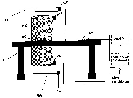
Figure 21 shows an embodiment of the invention as used in a fabricating
system. In this
embodiment, the fabricating system comprises a wafer stage 400, a reticle
stage 402, laser
interferometers 404, 404', 404", and 404"' with X&Y mirrors, and a support
structure 406. The
support structure 406 supports a lens assembly 410. The interferometers 404,
404', 404", and
404"' are located on the wafer stage 400, the reticle stage 402, and on the
lens assembly 410.
Mounted on the support structure 406 are two actuators 408 and 408'
comprising, for example,
an electroactive element. Each of the actuators 408 and 408' are in electrical
communication
with a circuit. Signals from the interferometers 404, 404', 404", and 404"'
are relayed through an
SBC analog UO channel and amplifiers to the actuators 408 and 408', which, in
response,
controls vibration within the fabricating system. By controlling the vibration
within the
fabricating system, the accuracy of the placement and absolute size of the
metallized traces in the
semiconductor on a wafer stage may be improved. Alternatively or in addition,
the through-put
of the fabrication system may be increased without decreasing accuracy.
Useful in this invention are electroactive actuator assemblies. Figure 1 A
illustrates in
schema the process and overall arrangement of a prior art surface mounted
piezoelectric actuator
CA 02359225 2001-07-27
WO 00/45067 PCTIUSOO/02251
-10-
assembly 10. A structure 20, which may be a structural or machine element, a
plate, airfoil or
other interactive sheet, or a device or part thereof has a sheet 12 of smart
material bonded thereto
by some combination of conductive and structural polymers, 14, 16. An
insulator 18, which may
be formed entirely or in part of the structural polymer 16, encloses and
protects the smart
material, while conductive leads or surface electrodes are formed or attached
by the conductive
polymer. An external control system 30 provides drive signals along lines 32a,
32b to the smart
material, and may receive measurement signals from surface-mounted
instrumentation such as a
strain gauge 35, from which it derives appropriate drive signals. Various
forms of control are
possible. For example, the strain gauge may be positioned to sense the
excitation of a natural
resonance, and the control system 30 may simply actuate the PZT element in
response to a sensor
output, so as to stiffen the structure, and thereby shift its resonant
frequency. Alternatively, a
vibration sensed by the sensor may be fed back as a processed phase-delayed
driving signal to
null out an evolving dynamic state, or the actuator may be driven for motion
control. In better-
understood mechanical systems, the controller may be programmed to recognize
empirical
conditions, i.e., aerodynamic states or events, and to select special control
laws that specify the
gain and phase of a driving signal for each actuator 12 to achieve a desired
change.
For all such applications, major work is required to attach the bare PZT plate
to its
control circuitry and to the workpiece, and many of the assembly steps are
subject to failure or,
when quantitative control is desired, may require extensive modeling of the
device after it has
been assembled, in order to establish control parameters for a useful mode of
operation that are
appropriate for the specific thicknesses and mechanical stiffnesses achieved
in the fabrication
process. A benefit of packaging an electroactive element when bonding to the
plate is that
electrical isolation or capacitive decoupling from the plate, structure or any
part of the fabrication
system may be achieved.
FIGURE 1B shows an actuator assembly useful in one embodiment of the present
invention. As shown, it is a modular pack or card 40 that simply attaches to a
structure 20 with a
quick setting adhesive, such as a five-minute epoxy 13, or in other
configurations attaches at a
point or line. The operations of sensing and control thus benefit from a more
readily installable
and uniformly modeled actuator structure. In particular, the modular pack 40
has the form of a
card, a stiff but bendable plate, with one or more electrical connectors
preferably in the form of
CA 02359225 2001-07-27
WO 00/45067 PCT/USOO/02251
-11-
pads located at its edge (not shown) to plug into a multi-pin socket so that
it may connect to a
simplified control system 50. As discussed in greater detail below with
respect to FIGURE 2C,
the modular package 40 may also incorporate planar or low-profile circuit
elements, which may
include signal processing elements, such as weighting or shunting resistors,
impedance matchers,
filters and signal conditioning preamplifiers, and may further include
switching transistors and
other elements to operate under direct digital control, so that the only
external electrical
connections necessary are those of a microprocessor or logic controller, and a
power supply.
In a further embodiment particularly applicable to some low power control
situations, a
modular package 60 as shown in Figure 1 C may include its own power source,
such as a battery
or power cell, and may include a controller, such as a microprocessor chip or
programmable
logic array, to operate on-board drivers and shunts, thus effecting a complete
set of sensing and
control operations without any external circuit connections.
The present invention specifically pertains to piezoelectric polymers, and to
materials
such as sintered metal zirconate, niobate crystal or similar piezoceramic
materials that are stiff,
yet happen to be quite brittle. It also pertains to electrostrictive
materials. As used in the claims
below, both piezoelectric and electrostrictive elements, in which the material
of the elements has
an electromechanical property, will be referred to as electroactive elements.
High stiffness is
essential for efficiently transferring strain across the surface of the
element to an outside structure
or workpiece, typically made of metal or a hard structural polymer, and the
invention in its
actuator aspect does not generally contemplate soft polymer piezoelectric
materials. While the
terms "stiff' and "soft" are relative, it will be understood that in this
context, the stiffness, as
applied to an actuator, is approximately that of a metal, cured epoxy, high-
tech composite, or
other stiff material, with a Young's modulus greater than .1 x 106, and
preferably greater than .2
x 106. When constructing sensors, instead of actuators, the invention also
contemplates the use
of low-stiffness piezoelectric materials, such as polyvinylidene difluoride
(PVDF) film and the
substitution of lower cure temperature bonding or adhesive materials. The
principal construction
challenges, however, arise with the first class of piezo material noted above,
and these will now
be described.
In general, the invention includes novel forms of actuators and methods of
making such
actuators, where "actuator" is understood to mean a complete and mechanically
useful device
CA 02359225 2001-07-27
WO 00/45067 PCT/US00/02251
-12-
which, when powered, couples force, motion or the like to an object or
structure. In its broad
form, the making of an actuator involves "packaging" a raw electroactive
element to make it
mechanically useful. By way of example, raw electroactive piezoelectric
materials or "elements"
are commonly available in a variety of semi-processed bulk material forms,
including raw
piezoelectric material in basic shapes, such as sheets, rings, washers,
cylinders and plates, as well
as more complex or composite forms, such as stacks, or hybrid forms that
include a bulk material
with a mechanical element, such as a lever. These materials or raw elements
may have metal
coated on one or more surfaces to act as electrical contacts, or may be non-
metallized. In the
discussion below, piezoelectric materials shall be discussed by way of
example, and all these
forms of raw materials shall be referred to as "elements", "materials", or
"electroactive
elements". As noted above, the invention further includes structures or
devices made by these
methods and operating as transducers to sense, rather than actuate, a strain,
vibration, position or
other physical characteristic, so that where applicable below, the term
"actuator" may include
sensing transducers.
Embodiments of the invention employ these stiff electrically-actuated
materials in thin
sheets - discs, annuli, plates and cylinders or shells - that are below
several millimeters in
thickness, and illustratively about one fifth to one quarter millimeter thick.
Advantageously, this
thin dimension allows the achievement of high electric field strengths across
a distance
comparable to the thickness dimension of the plate at a relatively low overall
potential
difference, so that full scale piezoelectric actuation may be obtained with
driving voltages of ten
to fifty volts, or less. Such a thin dimension also allows the element to be
attached to an object
without greatly changing the structural or physical response characteristics
of the object.
However, in the prior art, such thin elements are fragile, and may break due
to irregular stresses
when handled, assembled or cured. The impact from falling even a few
centimeters may fracture
a piezoceramic plate, and only extremely small bending deflections are
tolerated before breaking.
In accordance with the present invention, the thin electrically actuated
element is encased
by layers of stiff insulating material, at least one of which is a tough film
which has patterned
conductors on one of its surfaces, and is thinner than the element itself. A
package is assembled
from the piezo elements, insulating layers, and various spacers or structural
fill material, such
that altogether the electrodes, piezo element(s), and enclosing films or
layers form a sealed card
CA 02359225 2001-07-27
WO 00/45067 PCT/US00/02251
-13-
of a thickness not substantially greater than that of the bare actuating
element. Where elements
are placed in several layers, as will be described below, the package
thickness is not appreciably
greater than the sum of the thicknesses of the stacked actuating elements.
FIGURE 2A illustrates a basic embodiment 100 of the invention. A thin film 110
of a
highly insulating material, such as a polyimide material, is metallized,
typically copper clad, on
at least one side, and forms a rectangle which is coextensive with or slightly
larger than the
finished actuator package. A suitable material available for use in
fabricating multilayer circuit
boards is distributed by the Rogers Corporation of Chandler, Arizona as their
Flex-I-Mid 3000
adhesiveless circuit material, and consists of a polyimide film formed on a
rolled copper foil. A
range of sizes are available commercially, with the metal foils being of 18 to
70 micrometer
thickness, integrally coated with a polyimide film of 13 to 50 micrometer
thickness. Other
thicknesses may be fabricated. In this commercial material, the foil and
polymer film are directly
attached without adhesives, so the metal layer may be patterned by
conventional masking and
etching, and multiple patterned layers may be built up into a multilayer board
in a manner
described more fully below, without residual adhesive weakening the assembly
or causing
delamination. The rolled copper foil provides high in-plane tensile strength,
while the polyimide
film presents a strong, tough and defect-free electrically insulating barrier.
In constructions described below, the film constitutes not only an insulator
over the
electrodes, but also an outer surface of the device. It is therefore required
to have high dielectric
strength, high shear strength, water resistance and an ability to bond to
other surfaces. High
thermal resistance is necessary in view of the temperature cure used in the
preferred fabrication
process, and is also required for some application environments. In general,
polyamide/imides
have been found useful, but other materials, such as polyesters or
thermoplastics with similar
properties, may also be used.
In the present constructions, the foil layer is patterned by conventional
masking and etch
techniques (for example, photoresist masking and patterning, followed by a
ferric chloride etch),
to form electrodes for contacting the surface of piezo plate elements.
Alternatively, a more
ductile, thin conductive layer may be used. For example, a thin conductive
layer may be printed
on the polymer film or directly on the piezoelectric element using silver
conductive ink. In
FIGURE 2A, electrodes 111 extend over one or more sub-regions of the interior
of the rectangle,
CA 02359225 2001-07-27
WO 00/45067 PCT/USOO/02251
-14-
and lead to reinforced pads or lands l 11 a, 111 b extending at the edge of
the device. The
electrodes are arranged in a pattern to contact a piezoelectric element along
a broadly-turning
path, which crosses the full length and width of the element, and thus assures
that the element
remains connected despite the occurrence of a few cracks or local breaks in
the electrode or the
piezo element. Frame members 120 are positioned about the perimeter of sheet
110, and at least
one piezoelectric plate element 112 is situated in the central region so that
it is contacted by the
electrodes I 11. The frame members serve as edge binding, so that the thin
laminations do not
extend to the edge, and they also function as thickness spacers for the hot-
press assembly
operation described further below, and as position-markers which define the
location of piezo
plates that are inserted during the initial stages of assembling the laminated
package.
FIGURE 2A is a somewhat schematic view, inasmuch as it does not show the layer
structure of the device which secures it together, including a further semi-
transparent top layer
116 (FIGURE 2B), which in practice extends over the plate 112 and together
with the spacers
120 and sheet 110 closes the assembly. A similar layer 114 is placed under the
piezo element,
with suitable cut-outs to allow the electrodes 111 to contact the element.
Layers 114, 116 are
preferably formed of a curable epoxy sheet material, which has a cured
thickness equal to the
thickness of the metal electrode layer, and which acts as an adhesive layer to
join together the
material contacting it on each side. When cured, this epoxy constitutes the
structural body of the
device, and stiffens the assembly, extending entirely over a substantial
portion of the surface of
the piezo element to strengthen the element and arrest crack growth, thereby
enhancing its
longevity. Furthermore, epoxy from this layer actually spreads in a
microscopically thin but
highly discontinuous film, about .0025 mm thick, over the electrodes, bonding
them firmly to the
piezo plate, but with a sufficient number of voids and pinholes so that direct
electrical contact
between the electrodes and piezo elements still occurs over a substantial and
distributed contact
area.
FIGURE 2B shows a cross-sectional view, not drawn to scale, of the embodiment
of
FIGURE 2A. By way of rough proportions, taking the piezoelectric plate 112 as
.2 - .25
millimeters in thickness, the insulating film 110 is much thinner, no more
than one-tenth to one-
fifth the plate thickness, and the conductive copper electrode layer 1 l l may
have a thickness
typically of ten to fifty microns, although the latter range is not a set of
strict limits, but
CA 02359225 2001-07-27
WO 00/45067 PCTIUSOO/02251
- 15-
represents a useful range of electrode thicknesses that are electrically
serviceable, convenient to
manufacture and not so thick as to either impair the efficiency of strain
transfer or introduce
delamination problems. The structural epoxy 114 fills the spaces between
electrodes 111 in each
layer, and has approximately the same thickness as those electrodes, so that
the entire assembly
forms a solid block. The spacers 120 are formed of a relatively compressible
material, having a
low modulus of elasticity, such as a relatively uncrosslinked polymer, and,
when used with a
pressure-cured epoxy as described below, are preferably of a thickness roughly
equivalent to the
piezoceramic plate or stack of elements, so that they form an edge binding
about the other
components between the top and bottom layers of film 110.
A preferred method of manufacture involves applying pressure to the entire
package as
the layer 116 cures. The spacers 120 serve to align the piezoceramic plates
and any circuit
elements, as described below with reference to FIGURES 3-5, and they form a
frame that is
compressed slightly during assembly in the cure step, at which time it may
deform to seal the
edges without leaving any stress or irregularities. Compression eliminates
voids and provides a
dense and crack-free solid medium, while the curing heat effects a high degree
of cross-linking,
resulting in high strength and stiffness.
An assembly process for the embodiment of FIGURES 2A, 2B is as follows. One or
more pieces of copper clad polyimide film, each approximately .025 to .050
millimeters thick in
total, are cut to a size slightly larger than the ultimate actuator package
dimensions. The copper
side of the film is masked and patterned to form the desired shape of
electrodes for contacting a
piezo element together with conductive leads and any desired lands or access
terminals. A
pitchfork electrode pattern is shown, having three tines which are positioned
to contact the center
and both sides of one face of a piezo element, but in other embodiments an H-
or a comb-shape
is used. The patterning may be done by masking, etching and then cleaning, as
is familiar from
circuit board or semiconductor processing technology. The masking is effected
by photoresist
patterning, screening, tape masking, or other suitable process. Each of these
electroded pieces of
polyimide film, like a classical printed circuit board, defines the positions
of circuit elements or
actuator sheets, and will be referred to below simply as a "flex circuit."
However, methods and
devices of the invention also contemplate using an electroded piezo element,
an insulator, and
electrical contacts, rather than a "flex circuit".
CA 02359225 2001-07-27
WO 00/45067 PCT/US00/02251
-16-
Next, uncured sheet epoxy material having approximately the same thickness or
slightly
thicker than the electrode foil layer is cut, optionally with through-
apertures matching the
electrode pattern to allow enhanced electrical contact when assembled, and is
placed over each
flex circuit, so it adheres to the flex circuit and forms a planarizing layer
between and around the
electroded portions. The backing is then removed from the epoxy layers
attached to the flex
circuits, and pre-cut spacers 120 are placed in position at corner and edges
of the flex circuit.
The spacers outline a frame which extends above the plane of the electrodes,
and defines one or
more recesses into which the piezo elements are to be fitted in subsequent
assembly steps. The
piezo element or elements are then placed in the recesses defined by the
spacers, and a second
electroded film 111, 112 with its own planarizing/bonding layer 114 is placed
over the element
in a position to form electrode contacts for the top of the piezo element. If
the device is to have
several layers of piezo elements, as would be the case for some bending
actuator constructions,
these assembly steps are repeated for each additional electroded film and
piezoelectric plate,
bearing in mind that a polyimide film which is clad and patterned on both
sides may be used
when forming an intermediate electrode layer that is to contact actuator
elements both above and
below the intermediate sheet.
Once all elements are in place, the completed sandwich assembly of patterned
flex
circuits, piezo sheets, spacers and curable patterned epoxy layers is placed
in a press between
heated platens, and is cured at an elevated temperature and pressure to harden
the assembly into a
stiff, crack-free actuator card. In a representative embodiment, a cure cycle
of thirty minutes at
350 F and 50-100 psi pressure is used. The epoxy is selected to have a curing
temperature below
the depoling temperature of the piezo elements, yet achieve a high degree of
stiffness.
The above construction illustrates a simple actuator card having a single
piezo plate
sandwiched between two electroded films, so that the plate transfers shear
strain efficiently
through a thin film to the surface of the actuator card. The measure of
transfer efficiency, given
by the shear modulus divided by layer thickness squared, and referred to as
gamma (F), depends
on the moduli and thickness of the epoxy 114, the rolled foil electrodes 111,
and the polyimide
film 110. In a representative embodiment in which the epoxy and copper
electrode layers are 1.4
mils thick and the epoxy has a modulus of .5x106, a gamma of approximately
9x10¹⁰
pounds/inch4 is achieved. Using a thinner epoxy layer and film with .8 mil
foil, substantially
CA 02359225 2001-07-27
WO 00/45067 PCT/US00/02251
-17-
higher F is achieved. In general, the gamma of the electrode/epoxy layer is
greater than 5x10¹⁰
pounds/inch4, while that of the film is greater than 2x10¹⁰ pounds/inch4.
It should be noted that using PZT actuator plates ten mils thick, a card
having two PZT
plates stacked over each other with three flex circuit electroded film layers
(the middle one being
double clad to contact both plates) has a total thickness of 28 mils, only
forty percent greater than
the plates alone. In terms of mass loading, the weight of the actuator
elements represents 90% of
the total weight of this assembly. Generally, the plates occupy fifty to
seventy percent of the
package thickness, and constitute seventy to ninety percent of its mass, in
other constructions.
Thus, the actuator itself allows near-theoretical performance modeling. This
construction offers
a high degree of versatility as well, for implementing benders (as just
described) as well as stacks
or arrays of single sheets.
Another useful performance index of the actuator constructed in accordance
with the
present invention is the high ratio of actuator strain s to the free piezo
element strain A, which is
approximately (.8) for the two layer embodiment described herein, and in
general is greater than
(.5). Similarly, the ratio of package to free element curvatures, K, is
approximately .85 - .90 for
the described constructions, and in general is greater than .7.
Thus, overall, the packaging involved in constructing a piezo element embedded
in a flex
circuit impairs its weight and electromechanical operating characteristics by
well under 50%, and
as little as 10%, while profoundly enhancing its hardiness and mechanical
operating range in
other important respects. For example, while the addition of sheet packaging
structure to the
base element would appear to decrease attainable K, in practical use the flex
card construction
results in piezo bender constructions wherein much greater total deflection
may be achieved,
since large plate structures may be fabricated and high curvature may be
repeatedly actuated,
without crack failure or other mechanical failure modes arising. Several
Figures will illustrate
the variety of constructions to which such enhanced physical characteristics
are brought.
First, the structure of an electroactive element embedded between flex
circuits not only
provides a low mass unified mechanical structure with predictable response
characteristics, but
also allows the incorporation of circuit elements into or onto the actuator
card. FIGURE 2C
shows a top view of one device 70 of this type, wherein regions 71, 73 each
contain broad
CA 02359225 2001-07-27
WO 00/45067 PCT/US00/02251
- 18-
electroactive sheets, while a central region 72 contains circuit or power
elements, including a
battery 75, a planar power amplification or set of amplifiers 77, a
microprocessor 79, and a
plurality of strain gauges 78. Other circuit elements 82a, 82b may be located
elsewhere along the
path of circuit conductors 81 about the periphery. As with the other
embodiments, spacers 120
define layout and seal edges of the device, while electrodes 111 attach the
electroactive elements
to the processing or control circuitry which is now built-in. The circuit
elements 82a, 82b may
comprise weighting resistors if the device is operated as a sensor, or
shunting resistors to
implement passive damping control. Alternatively, they may be filtering,
amplifying, impedance
matching or storage elements, such as capacitors, amplifiers or the like. In
any case, these
elements also are located away from electroactive plates 84. The components
collectively may
sense strain and implement various patterns of actuation in response to sensed
conditions, or
perform other sensing or control tasks.
Returning now to the actuator aspect of the invention, FIGURE 3 shows a top
view of an
actuator package 200 having dimensions of about 1.25 x 9.00 x.030 inches and
assembled with
two layers of piezoelectric plates of four plates each. A rectangular
polyimide sheet 210 with an
end tab 210a carries an electrode 211 in the form of a lattice of H-shaped
thin copper lines
interconnected to each other and to a single runner 211 a that leads out to
the tab, thus providing a
low impedance connection directly to each of four rectangular regions which
hold the piezo
plates.
Spacer elements 220a, 220b of H-shape, or 220c of L-shape mark off corners and
delineate the rectangular spaces for location of the piezo plates 216. In this
embodiment, a
plurality of gaps 230, discussed further below, appear between adjacent the H-
or L- spacers. As
will be apparent from the description below, the use of these small discrete
spacer elements (I-,
T- or 0-shaped spacers may also be convenient) is enhanced because they may be
readily placed
on the tacky bonding epoxy layer 114 during assembly to mark out assembly
positions and form
a receiving recess for the piezo elements. However, the spacer structure is
not limited to such a
collection of discrete elements, but may be a single or couple of frame
pieces, formed as a
punched-out sheet or molded frame, to provide all, or one or more, orienting
and/or sealing
edges, or recesses for holding actuation of circuit components.
CA 02359225 2001-07-27
WO 00/45067 PCTIUSOO/02251
- 19-
FIGURE 5 illustrates a top view of each of the three sheet, electrode and
piezo plate
layers separately, while FIGURE 5A illustrates the general layering sequence
of the film,
conductor, and spacer/piezo layers. As shown, the spacers 220 and piezo plates
216 constitute a
single layer between each pair of electrode layers.
FIGURES 4A and 4B (not drawn to scale) illustrate the layer structure of the
assembled
actuator along the vertical sections at the positions indicated by "A" and "B"
in FIGURE 3. As
more clearly shown in FIGURE 4A, a patterned bonding layer of epoxy sheet 214
is coplanar
with each electrode layer 211 and fills the space between electrodes, while
the spacer 220c is
coplanar with the piezo plate 216 and substantially the same thickness as the
plate or slightly
thicker. Illustratively, the piezo plate 216 is a PZT-5A ceramic plate,
available commercially in
a five to twenty mil thickness, and has a continuous conductive layer 216a
covering each face for
contacting the electrodes 211. The spacers 220 are formed of somewhat
compressible plastic
with a softening temperature of about 250 C. This allows a fair degree of
conformability at the
cure temperature so the spacer material may fill slight voids 214a (FIGURE 4A)
during the
assembly process. As shown in FIGURE 4B, the gaps 230 (when provided) between
spacers
result in openings 214b which vent excess epoxy from the curable bonding
layers 214, and fill
with epoxy during the cure process. As illustrated in that FIGURE, a certain
amount of epoxy
also bleeds over into patches of film 215 between the electrodes 211 and the
piezo plate 216.
Because of the large and continuous extent of electrode 211, this patchy
leakage of epoxy does
not impair the electrical contact with the piezo elements, and the additional
structural connection
it provides helps prevent electrode delamination.
It will be appreciated that with the illustrated arrangements of electrodes,
each vertically
stacked pair of piezo plates may be actuated in opposition to each other to
induce bending, or
more numerous separate electrodes may be provided to allow different pairs of
plates to be
actuated in different ways. In general, as noted above, the invention
contemplates even quite
complex systems involving many separate elements actuated in different ways,
with sensing,
control, and power or damping elements all mounted on the same card. In this
regard, great
flexibility in adapting the card to practical tasks is further provided by its
flexibility. In general,
it has a supple flexibility comparable to that of an epoxy strip thirty mils
thick, so that it may be
bent, struck or vibrated without damage. It may also be sharply bent or curved
in the region of
CA 02359225 2001-07-27
WO 00/45067 PCTIUSOO/02251
-20-
its center line CL (FIGURE 3) where no piezo elements are encased, to conform
to an attaching
surface or corner. The elements may be poled to change dimension in-plane or
cross-plane, and
the actuators may therefore be attached to transmit strain to an adjacent
surface in a manner
effective to perform any of the above-described control actions, or to launch
particular
waveforms or types of acoustic energy, such as flexural, shear or
compressional waves into an
adjacent surface.
FIGURE 6 shows another actuator embodiment 300. In this embodiment,
illustrated
schematically, the epoxy bonding layer, film and spacer elements are not
shown, but only
electrode and piezo sheets are illustrated to convey the operative mechanisms.
A first set of
electrodes 340 and second set 342 are both provided in the same layer, each
having the shape of
a comb with the two combs interdigitated so that an electrical actuation field
is set up between
the tooth of one comb and an adjacent tooth of the other comb. In FIGURE 6, a
parallel pair of
combs 340a, 342a is provided on the other side of the piezo sheet, with comb
electrode 340 tied
to 340a, and comb electrode 342 tied to 342a, so as to set up an electric
field with equipotential
lines "e" extending through the piezo sheet, and in-plane potential gradient
between each pair of
teeth from different combs. In the embodiment shown, the piezoceramic plates
are not
metallized, so direct electrical contact is made between each comb and the
plate. The plates are
poled in-plane, by initially applying a high voltage across the combs to
create a field strength
above one two thousand volts per inch directed along the in-plane direction.
This orients the
piezo structure so that subsequent application of a potential difference
across the two-comb
electrodes results in in-plane (shear) actuation. Thus, the direct contact of
interdigital electrodes
provides to the piezo element an electrical field which is generally parallel
to the actuation
direction.
In addition to shear actuation, directional actuation and damping may be
effected using
methods or devices of the invention. For example, as shown in FIGURE 7, two
such actuators
300 may be crossed to provide torsional actuation.
In discussing the embodiments above, the direct transfer of strain energy
through the
electrode/polyimide layer to any adjoining structure has been identified as a
distinct and novel
advantage. Such operation may be useful for actuation tasks or diverse as
airfoil shape control
actuation and noise or vibration cancellation or control. FIGURES 8A and 8B
illustrates typical
CA 02359225 2001-07-27
WO 00/45067 PCT/US00/02251
-21 -
installations of flat (FIGURE 8A) and hemicylindrical (FIGURE 8B) embodiments
60 of the
actuator, applied to a flat or slightly curved surface, and a shaft,
respectively.
However, while the electromechanical materials of these actuators operate by
strain
energy conversion, applications of the present invention extend beyond strain-
coupling through
the actuator surface, and include numerous specialized mechanical
constructions in which the
motion, torque or force applied by the actuator as a whole is utilized. In
each of these
embodiments, the basic strip- or shell-shaped sealed actuator is employed as a
robust, springy
mechanical element, pinned or connected at one or more points along its
length. As shown in
FIGURE 9, when electrically actuated, the strip then functions, alone or with
other elements, as a
self-moving lever, flap, leaf spring, stack or bellows. In the diagrams of
FIGURES 9(a) - 9(q),
the elements A, A', A" . . . are strip or sheet actuators such as shown in the
above FIGURES,
while small triangles indicate fixed or pinned positions which correspond, for
example, to rigid
mounting points or points of connection to a structure. Arrows indicate a
direction of movement
or actuation or the contact point for such actuation, while L indicates a
lever attached to the
actuator and S indicates a stack element or actuator.
The configurations of FIGURES 9(a)-9(c) as stacks, benders, or pinned benders
may
replace many conventional actuators. For example, a cantilevered beam may
carry a stylus to
provide highly controlled single-axis displacement to constitute a highly
linear, large
displacement positioning mechanism of a pen plotter. Especially interesting
mechanical
properties and actuation characteristics are expected from multi-element
configurations 9(d) et
seq., which capitalize on the actuators having a sheet extent and being
mechanically robust.
Thus, as shown in FIGURES 9(d) and (e), a pin-pin bellows configuration may be
useful for
extended and precise one-axis Z-movement positioning, by simple face-
contacting movement,
for applications such as camera focusing; or may be useful for implementing a
peristalsis-type
pump by utilizing the movement of the entire face bearing against a fluid. As
noted in
connection with FIGURE 3, the flex circuit is highly compliant, so hinged or
folded edges may
be implemented by simply folding along positions such as the centerline in
FIGURE 3, allowing
a closed bellows assembly to be made with small number of large, multi-element
actuator units.
The flex circuit construction allows strips or checkerboards of actuator
elements to be laid out
with fold lines between each adjacent pair of elements, and the fold lines may
be impressed with
CA 02359225 2001-07-27
WO 00/45067 PCTIUSOO/02251
-22-
a thin profile by using a contoured (e.g. waffle-iron) press platen during the
cure stage. With
such a construction, an entire seamless bellows or other folded actuator may
be made from a
single flex circuit assembly.
As noted above, the piezo element need not be a stiff ceramic element, and if
the flex
circuit is to be used only as a sensor, then either a ceramic element, or a
soft material such as
PVDF may be employed. In the case of the polymer, a thinner more pliant low
temperature
adhesive is used for coupling the element, rather than a hard curable epoxy
bonding layer.
Certain embodiments of the invention are exemplified below.
EXAMPLE 1
In this example, a vibration control system was designed to determine certain
parameters
of functional requirements of a gantry active control system. The funtional
requirements defined
included (but were not limited to) the following:
= Accuracy
= Settling time
= Mass, size and location of the actuators and sensors
= Power
= Peak strains
= Lifetime
= Temperature range
= Exposure to humidity and solvents
= Cost
= Interfaces with existing gantry control system
In order to gather data on the structural response of a gantry during
operation, the gantry
was equipped with an array of piezoelectric strain sensors and accelerometers.
Placement and
sizing of the piezoelectric actuators required accurate strain mode shape
information, which were
obtained from this data, and were compared to the Finite Element Model
("FEM"). One
important piece of information obtained in this phase of the project involved
the effect of
different head positions on the dynamics. Both the actuator design and any
control software
design depended on when the vibration control was applied, i.e., while the
head was moving
along the gantry, and/or after it had stopped at an arbitrary position on the
gantry.
CA 02359225 2001-07-27
WO 00/45067 PCT/US00/02251
-23-
Data was acquired both with and without a friction block in place, to allow at
least
analytical evaluation of the potential for complete replacement of the
friction block by the
electroactive vibration control system.
Using the data acquired above, along with finite element modeling information,
the
system-level design was performed. This design involved selecting a system
architecture,
including actuator placement, type of sensor, and the type of control
algorithm. As discussed
above, with the moving head having a significant effect on the gantry
dynamics, the electroactive
vibration control system's effectiveness was improved by making the trajectory
information
available in the motion control system. This information may be relayed to the
motion control
system with a simple clip lead attached to the proper point in the motion
controller's circuitry.
For example, information such as the plots of motor current, which is often
easily accessible,
may be provided to the vibration control system.
After selecting the system architecture, an analytical "input/output" model of
the system
was developed, to design the control algorithm for vibration control, and to
simulate its
performance. The system design was compared to the functional requirements, to
ensure
compliance. This analysis served to define the specifications on the various
components of the
control system, especially the analog sensor signal conditioning electronics,
the digital signal
processor (DSP) based control unit, and the power amplifier used to provide
the necessary
voltage and current to the electroactive actuators.
Each of the components of the electroactive vibration control system were then
designed,
including the various electronic components. The electroactive actuators
themselves were
fabricated using methods disclosed herein. Each actuator was tested using
standard quality
control methods. All electronics were fabricated and tested for functionality
and for compliance
with the specifications devised in the system design task.
An important aspect of the design involved the integration of the actuators
and sensors
with the gantry. For example, for a given gantry, a 0.5 mm actuator thickness
may be determined
to not likely interfere with motion of the head along the gantry. The types of
cable used to
connect the actuators and sensor on the gantry to the electronic equipment
were then determined.
CA 02359225 2001-07-27
WO 00/45067 PCT/US00/02251
-24-
In this particular example, the gantry of an automated SMT electronics collect
and place
equipment was equipped with actuators, sensors and electronics, and anaylyzed
using an FEM
with plate elements. The basic concept, shown in block diagram in Figure 10,
includes
electroactive strain actuators and sensors bonded to the gantry, along with
the necessary power,
signal, and digital control electronics to achieve vibration reduction. For
the purposes of this
study, the head was assumed to be fixed at the end of the gantry. The
installation of actuators
was done using a vacuum-bonding procedure.
"Open loop" testing was then performed. Open loop testing involves injecting
signals
into the actuators and measuring the response of the gantry to confirm
experimentally the
analytical modeling done earlier in this study. This testing was performed
with the gantry and
head stationary, as well as moving along some "standard" trajectories. The
signal(s) to be passed
from the gantry and head motion controller to the vibration control system
were measured as well
during these tests. The electoactive actuators were distributed over 10% of
the surface area of
the gantry having the maximum strain energy in the first natural mode of
vibration. The
effectiveness of the actuator distribution at exciting the first three modes
of vibration was
modeled using design software. Between 80-84% of all strain energy is in the
plate elements;
and between 62-75% of the plates' energy is extensional strain, and therefore
available for
capture by electroactive control devices bonded to the surface. Thus, at least
52% of the strain
energy in a mode is available. Some of this energy is in the frame/support for
the moving head.
As shown in FIGURE 13, the extensional strain energy was sorted to maximize
performance for
a given amount of electroactive element.
Damping was added to the structural model. Plots of acceleration versus time
at the head,
after impact by a hammer, showed roughly 5% of critical damping in the first
mode with the
friction block in place.
Feedback control was designed using the standard Linear Quadratic Regulator
(LQR)
approach, ensuring that piezoelectric actuation control voltages did not
exceed the actuator
device limits. Actuation voltages in the closed feedback loop are proportional
to the input
disturbance forces associated with the motion of the gantry. Here, the gantry
was assumed to
accelerate in the y-direction (transverse to the gantry axis) at a constant 25
m/s2 until maximum
velocity of 3 m/s was reached. The D'Alembert inertial force associated with a
10 kg mass was
CA 02359225 2001-07-27
WO 00/45067 PCTIUSOO/02251
-25-
applied at the center of gravity of the head. This mass included the 5 kg head
mass, plus 5 kg of
effective gantry mass.
The improvements in damping and settling time were then determined after
simulating
the vibration-controlled system's frequency and time domain responses.
Frequency responses
are simulated in Figure 11, measured at a point on the underside of the pick
and place head, in
the y-direction. The reduction in dynamic response to a unit input force is
evident in this figure.
As shown in FIGURE 11, as well as Table I, mode 1 closed loop damping was
about 12%, mode
2 closed loop damping was about 11 %, and mode 3 closed loop damping was about
10%. Time
responses at the same point, in the same direction, are simulated in Figure
12. This simulation
shows a dramatic reduction in settling time with the electroactive control.
Thus, very effective
control can be achieved with very little additional mass.
Table I: Gantry structural dynamic parameters.
Inherent D. . . Ratio
Frequency D. . . Ratio with P - .
..- D- . . ', . . . 1 Twisting about gantry 46 5 12
axis
2 Bending in xy 93 5 11
(scanning) plane
3 Coupled bend/twist 136 5 10
The gantry/head structural dynamic properties, from FEM, are shown in Table I.
The
representative actuator distribution designed here was 0.5 mm thick, with an
area of 330 cm2, and
a mass of less than 100g. The closed loop modal damping, also shown in Table
I, was at least
twice the assumed 5% value inherent to the gantry with the friction block, for
all three modes of
vibration included in the analysis. Thus, the vibration amplitude and settling
time were
significantly reduced.
As shown in Figures 14 and 15, the vibration control system induced changes in
the
frequency response and gain control. In this study, the damping was increased
by over one order
of magnitude. This increase corresponds to an increase in placement accuracy
of a factor of ten.
Following the open loop tests, the data was analyzed and the final control
algorithm
design was performed. If necessary, the actuator and sensor hardware may be
modified to ensure
CA 02359225 2008-01-18
-26-
compliance with the functional requirements. Then, "closed loop" testing of
the final
electroactive vibration control system may be performed. Closed loop testing
is generally when
actuators are driven at least in part by signals generated by sensors.
This study demonstrated that effective active electroactive vibration control
of the gantry
is possible.
EXAMPLE 2
A vibration control system in accordance with the invention was used in a
lithography
machine. As shown in Figure 16, which shows the power spectral density of
error signals
recorded by a laser metrology system, use of the vibration control system
resulted in a three-fold
reduction in system response in the band from 75 to 125 Hz. The reduction in
the peak using the
vibration control system would be expected to reduce the system image blur by
a factor of two-
three after conventional methods are used to reduce peaks at 50 Hz and 225 Hz.
Alternatively, in
some cases, the vibration control system might be used to reduce the peaks at
50 Hz or 225 Hz or
at other levels. Reducing the image blur allows the fabrication system to
produce finer trace
dimensions and feature sizes and improves the accuracy of the feature
placement
The foregoing description of embodiments and examples of the present invention
are
presented to demonstrate the range of constructions to which the invention
applies. Those skilled
in the art will appreciate that many other modifications and variations of the
invention as set
forth hereinabove may be made without departing from the spirit and scope
thereof.