Note: Descriptions are shown in the official language in which they were submitted.
' _
, CA 02359473 2001-07-10
Method of electrolytically forming conductor structures from highly pure
copper when producing integrated circuits
Description:
The invention relates to a method of electrolytically forming conductor
structures from highly pure copper, for example conductor paths, through-
holes, connection contactings and connection places, on surfaces of
semiconductor substrates (wafers), which surfaces are provided with
recesses, when producing integrated circuits, more especially in cases where
the recesses have a high aspect ratio.
To produce integrated circuits, the so-called silicon planar technique is
used, wherein epitaxy and doping methods are employed. For such
purpose, monocrystaline silicon discs, so-called wafers, are processed by
physical methods in order to form variably conductive regions on the silicon
surface in the micrometer range and, for some time, also in the sub-
micrometer range (presently 0.25 Vim).
The production process can be divided into three steps:
(a) production of transistors and mutual oxidation thereof; this
process is also called FEOL (Front End of Line) ("Technoiogie
hochintegrierter Schaltungen", D.Widmann, H.Mader, H.Friedrich, 2nd
Edition, Springer-Verlag, 1996; "VLSI-Electronic Microstructure Science",
Norman G. Einspruch, Editor, more esp. Vol. 19 "Advanced CMOS
Technology", J.M.Pimbley, M.Ghezzo, H.G.Parks, D.M.Brown, Academic
Press, New York, 1989);
' . ., - CA 02359473 2001-07-10
2
(b) contacting and connection of the individual mono- and
polycrystalline silicon regions of the FOEL part according to the desired
integrated circuit;
(c) passivation or protection against mechanical damage or against
the penetration of foreign substances.
In the second step, the transistors are generally contacted by
multilayer metallisation and interconnected, the dielectric silicon dioxide
being
usually used for isolating the conductor tracks formed therefor.
To produce the conductor paths, the connection contacting holes and
the connection places, an aluminium layer, having a thickness generally of
1 Vim, has been applied for a long time by physical methods, for example a
vaporisation method (electron beam evaporation method) or a sputtering
method. Said layer is subsequently structured by suitable etching methods
using a photoresist.
Aluminium is described, in older literature, as the most advantageous
aitemative of the materials available for producing conductor paths,
connection contactings and connection places. For example, demands on
this layer are described in "Integrierte Bipolarschaltungen" by H.-M.Rein and
R.Ranfft, Springer-Veriag, Berlin, 1980. The problems mentioned there are
in fact minimised by specific method optimisations, but they cannot be
completely avoided.
More recently, it has been possible to replace aluminium by
electrolytically deposited copper (IEEE-Spektrum, January 1998, Linda
Geppert, "Solid State", Pages 23 to 28). Because of the greater electrical
conductance, the greater thermal resistance and the resistance to diffusion
' ' . , . CA 02359473 2001-07-10
3
and migration, more especially, copper has proved to be an alternative to
aluminium as the preferred material. For such purpose, the so-called
"Damaszene" technique is employed (IEEE-Spektrum, January 1998, Linda
Geppert, "Solid State°, Pages 23 to 28, and P.C. Andricacos et al. in
IBM J.
Res. Developm., Vol. 42. Pages 567 to 574). For such purpose, a dielectric
layer is initially applied to the semiconductor substrate. The required vias
and
trenches are etched to receive the desired conductor structures, usually by a
dry-etching method. After a diffusion barrier (mainly titanium nitride,
tantalum
or tantalum nitride) and a conductive layer (mainly sputtered copper) have
been applied, the recesses, i.e. the vias and trenches, are electrolytically
filled
by the so-called trench-~Iling process. Since, in such case, the copper is
deposited over the entire surface, the excess at the undesired locations has
to be subsequently removed again. This happens with the so-called CMP
process (Chemico-mechanical polishing). Multilayer circuits can be produced
by repeating , the process, i.e. repeated application of the dielectric (for
example of silicon dioxide) and formation of the recesses by etching.
The technical demands on the electrolytic copper deposition. process
are given hereinafter:
(a) Constant layer thickness over the entire wafer surface (planarity); the
smaller the deviations from the intended layer thickness, the easier is
the subsequent CMP process;
(b) Reliable trench-filling, even of very deep trenches, with a high aspect
ratio; in the future, aspect ratios of 1 : 10 are expected;
(c) Greatest possible electrical conductance and, hence, automatically the
greatest purity of the deposited copper; for example, it is necessary for
the sum of all of the impurities in the copper layer to be less than 100
ppm ( 0.01 % by wt.).
~
, CA 02359473 2001-07-10
It has become apparent that this technique for producing the conductor
paths, connection contactings and connection places presents advantages
over the aluminium used hitherto. However, disadvantages have now also
become apparent when using the plating method of prior art, and such
disadvantages lead to a reduction in the yield or, at least, to high costs for
the
production:
(a) When soluble anodes are used, it is disadvantageous for the
geometry of the anodes to change slowly during the deposition process, since
the anodes dissolve during the deposition process, with the result that it is
impossible to achieve any dimensional stability and, hence, also any constant
field line distribution between the anodes and the wafers. In order to
overcome this problem, at least partially, inert containers for chunky anode
material are in fact used, so that the dimensions of the anodes do not vary
too
much during the deposition process, and dissolved anodes can be replaced
again relatively easily. While these so-called anode baskets are being
supplemented with fresh anode material, however, the deposition process
has to be stopped, so that, when the process is started-up afresh, only test
samples can initially be processed because of the resultant changes in the
bath, in order to achieve constant stationary conditions of the process again.
Moreover, each change of anode leads to a contamination of the bath
because of impurities being separated from the anodes (anode slime). Also,
in consequence, a longer start-up time is required after the topping-up of
anodes.
(b) Moreover, copper which is dissolved in the bath weakens during
the copper deposition. If copper salts are then supplemented in the bath, this
leads to a variable content of copper in the solution. In turn, in order to
keep
such content constant, considerable outlay in respect of control engineering
has to be involved.
. , CA 02359473 2001-07-10
(c) Furthermore, when insoluble anodes are used, there is a risk of
gases being developed at the anodes. During the deposition process, these
gases separate from the anodes, which are usually kept horizontal, and rise
upwardly in the deposition solution. There, they encounter the wafers, which
are also usually kept horizontal and are situated opposite the anode, and they
precipitate on the lower surface of said wafers. The locations on the wafer
surface, on which the gas bubbles settle, are screened from the
homogeneous electrical field in the bath, so that no copper deposition can
occur there. The regions which are disturbed in such manner may lead to
the wafer or at least parts of the wafer being rejected.
(d) Moreover, insoluble anodes are destroyed when pulse
techniques are used, because the noble metal coatings are dissolved.
(e) Furthermore, no phase boundaries are allowed to form in the
copper-filled recesses because of a copper layer, which grows from the base
of the recesses and/or the lateral faces, or even cavities in the copper. This
has been described, for example, by P.C.Andricacos et al., ibid. An
improvement was achieved there by adding additives to the deposition bath,
which additives serve to improve the layer properties.
(f) An additional substantial disadvantage resides in the fact that
the applied copper layer has to be very flat. Since the copper layer is formed
both in the recesses and on the raised locations of the wafer, a copper layer
is produced, which has a very non-uniform thickness. When the Damaszene
technique is used, the surface is smoothed by the CMP method. In such
case, the increased polishing rate (dishing) over the structures (trenches and
vias) can be disadvantageous. The best result in the publication by
P.C.Andricacos et al., ibid is shown by a copper layer where there is another
CA 02359473 2001-07-10
8
slight indentation over the recesses. This indentation also leads to problems
during polishing.
In consequence, the basic object of the present invention is to avoid
the disadvantages of known methods and, more especially, to minimise the
increased contamination of the copper coatings obtained when the more
advantageous insoluble anodes are used. Moreover, it is desirable to
prevent electrolyte inclusions from forming in the copper structure when
forming the copper structures in recesses having a large aspect ratio.
Furthermore, the problems which result from supplementing the copper salts
in the deposition solution are to be solved. It is also very important to
overcome the dishing problem.
These problems are solved by the method according to claim 1.
Preferred embodiments of the invention are found in the sub-claims.
The method, according to the invention, for electrolytically forming
conductor structures from highly pure copper on the semiconductor
substrates (wafers) when producing integrated circuits includes the following
essential method steps:
a. filling the recesses, situated on the surfaces of the wafers, with a full-
surface basic metal layer, preferably having a thickness of between
0.02 ~m and 0.3 p,m, to produce sufficient conductance (plating base),
a physical metal deposition method andlor a CVD method and/or a
PECVD method preferably being used;
b. full-surface deposition of copper Payers with a uniform layer thickness
on the basic metal layer by an electrolytic metal deposition method in a
copper deposition bath,
' ' ~ , CA 02359473 2001-07-10
7
i. the copper deposition bath containing at least one copper ion
source, at least one additive compound for controlling the
physico-mechanical properties of the copper layers as well as
Fe(II) and/or Fe(III) compounds, and
ii. an electric voltage being applied between the wafers and
dimensionally stable counter-electrodes, which are insoluble in
the bath and brought into contact therewith, so that an electric
current flows between the wafers and the counter-electrodes,
and the electric voltage and the flowing current either being
constant or being changed per unit time in the form of uni- or
bipolar pulses;
a. structuring the copper layer, preferably by a CMP method.
With the method according to the invention, it is possible for the first
time to avoid, the disadvantages of the various known method variants for
producing integrated circuits.
It was surprisingly found that, by adding Fe(II)/Fe(Ia) compounds, not
only can the above-mentioned disadvantages (a) to (d) - as described in DE
195 45 231 A1 for use in printed circuit board technology - be overcome, but
that, contrary to every expectation, the purity of the copper layers is also
excellent and that, more especially, no iron is incorporated in the copper, so
that the deposited copper meets all specifications, more especially also the
demand for good trench-filling, a phenomenon for which there is hitherto no
plausible scientific explanation. The observation that even a somewhat
thicker metal layer was formed over the recesses than was formed over the
raised structures was particularly surprising, so that the disadvantageous
effect of "dishing" is compensated-for.
The advantages in detail:
~
CA 02359473 2001-07-10
8
(a) Contrary to all expectation, it was ascertained that the degree of
contamination of the copper structures produced when dimensionally stable,
insoluble anodes are used can be clearly reduced, although additional
ingredients, namely iron salts, are added to the deposition bath. Typically,
the copper only contains at most 10 ppm iron. The result which was found is
contrary to the expectation that, by adding additional substances to the
deposition bath, even more strongly contaminated coatings are usually
obtained. In consequence, there was hitherto the demand to use chemicals
which are as pure as possible for producing integrated circuits. Generally, in
fact, the basic concept is that highly pure chemicals should be used
exclusively for producing integrated circuits in order to prevent
contaminations
of the most highly sensitive silicon. This requirement is based on the fact
that the degree of contamination of the electrical regions in .an integrated
circuit is greater when the degree of contamination of the chemicals used to
produce the circuit is greater. Contamination of the electrical regions in the
silicon is to be avoided in any case since, even with the slightest impurity
of
these regions, disadvantageous consequences and probably even a total
failure of the circuit are to be feared.
Compared with production techniques for integrated circuits, not nearly
such high requirements for the purity of the copper layer are made in printed
circuit board technology. In consequence, the use of iron salts in this case
could be accepted without any problems.
Furthermore, it is known that iron from plating baths for depositing
copper alloys, which contain iron, is also deposited as alloy metal. For
example, in "Electrodeposition of high Ms cobalt-iron-copper alloys for
recording heads", J.W.Chang, P.C.Andricacos, B.Petek, L.T.Romankiw, Proc.
- Electrochem. Soc. (1992), 92-10 (Proc. Int. Symp. Magn. Mater.
CA 02359473 2001-07-10
9
Processes, Devices, 2"°, 1991 ), Pages 275 to 287, for the
deposition of an
alloy, containing copper and iron, it is described that a content of iron in
the
deposition bath (15 g/I FeS04 ~7 H20), which substantially corresponds to the
iron content in the copper deposition bath according to the invention, leads
to
a considerable iron content in the alloy. Reference is also made to the
electrolytic deposition of iron-containing alloys in other publications, for
example in "pH-changes at the cathode during electrolysis of nickel, iron, and
copper and their alloys and a simple technique for measuring pH changes at
electrodes", L.T.Romankiw, Proc. - Eiectrochem. Soc. (1987), 87-17 (Proc.
Symp. Electrodeposition Technol., Theory Pract.), 301-25.
(b) A very uniform copper layer thickness at all locations of the
wafer is also achieved.
Recesses with a usually very small width, or respectively with a very
small diameter, are very rapidly completely filled with metal. A somewhat
greater thickness of the metal is even achieved over such recesses than is
achieved over the raised structures. In consequence, the outlay for the
subsequent polishing by the CMP method is not very great. The recesses
generally have a width or a diameter of between 0.15 ~,m and 0.5 Vim. The
depth thereof is usually substantially 1 p,m.
Contrary to known methods, the copper layers obtained by a
production according to the method of the invention are equally thick at the
leading edges to the recesses to be metallised as at the lateral walls and at
the base of the recesses in the case where recesses have greater Lateral
dimensions. The copper layer largely follows the surface contour of the
wafer surface. The disadvantage is thus avoided, where the cross-section of
the recesses at the upper edge is already completely filled with copper, white
deposition solution is still situated in the lower region of the recesses. The
~
CA 02359473 2001-07-10
problems which arise with such an inclusion of electrolyte, for example an
explosion-like escape of the included fluid during heating of the circuit,
diffusion of impurities through the copper, are thus completely avoided. A
metal structure is obtained, which is uniformly filled with copper and meets
the
usual requirements which exist for the production of integrated circuits.
(c) Furthermore, the disadvantages which arise when soluble (copper)
anodes are used can be avoided. A reproducible field line distribution within
the deposition bath is achieved, more especially. However, the geometry of
soluble anodes constantly changes because of the dissolution, so that no
time-stable field line distribution can be obtained, at least in the outer
region
of the wafers situated opposite the anodes. By using the dimensionally
stable anodes, therefore, it is now possible to produce even greater wafers
than hitherto.
The problems which occur when supplementing used anode material
(contamination of the bath by anode slime and by other impurities, operational
interruptions by disconnection of the bath and renewed starting and charging
of the bath) can also be avoided when insoluble anodes are used.
(d) It is also surprising that, with the method according to the
invention, recesses having very high aspect ratios can easily be filled with
copper without gas or liquid inclusions being formed in the copper conductor
track. A scientific explanation for this phenomenon had hitherto not yet been
found.
It was also observed that many electrolytes have a surprisingly good
trench-filling behaviour, while such a result could not be achieved with other
electrolytes.
CA 02359473 2001-07-10
11
A pulse current or pulse voltage method is preferably used. In the
pulse current method, the current between the workpieces, polarised as the
cathode, and the anodes is set galvanostatically and modulated per unit time
by suitable means. In the pulse voltage method, a voltage between the
wafers and the counter-electrodes (anodes) is set potentiostaticaily, and the
voltage is modulated per unit time so that a current is set which is variable
per
unit time.
The method, which is known from technology as the reverse pulse
method, is preferably used with bipolar pulses. Those methods are
especially suitable, in which the bipolar pulses comprise a sequence of
cathodic pulses, lasting from 20 milliseconds to 100 milliseconds, and anodic
pulses lasting from 0.3 milliseconds to 10 milliseconds. In a preferred use,
the peak cun-ent of the anodic pulses is set to at least the same value as the
peak current of the cathodic pulses. The peak current of the anodic pulses is
preferably set two to three times as high as the peak current of the cathodic
pulses.
(e) Gas bubbles are also prevented from developing on the insoluble
anodes. The problems, which arise when known methods are used with the
precipitation of these gas bubbles on the wafers situated opposite the
anodes, are avoided because water is not decomposed as the anode reaction
according to
2H20 -~ 02 + H+ + 4e-
but the reaction
Fe2+ -~ Fe3+ + e'
~
' , CA 02359473 2001-07-10
12
occurs. In consequence, an electric screening of individual regions on the
wafer surfaces does not occur during the copper deposition, so that an
improved yield is achieved as a general rule during the production of the
integrated circuits. Furthermore, less electrical energy is also required.
According to the invention, a method of producing a full-surface, highly
pure copper layer on semiconductor substrates (wafers), provided with
recesses, is also available, wherein the above method steps a. and b. are
carried out. A structuring of the copper layer according to method step c. is
omitted in this case. The above-mentioned advantages also apply to the
production of a full-surface copper layer, since conductor structures can
easily
be produced from such layer by known methods.
Besides containing at least one copper ion source, preferably a copper
salt with an inprganic or organic anion, for example copper sulphate, copper
methane sulphonate, copper, pyrophosphate, copper fluoroborate or copper
sulphamate, the bath used for the copper deposition additionally contains at
least one substance for increasing the electrical conductance of the bath, for
example sulphuric acid, methane sulphonic acid, pyrophosphoric acid,
fluoroboric acid or amidosulphuric acid.
Typical concentrations of these basic ingredients are given hereinafter:
copper sulphate (CuS04 ~ 5 H20) 20 - 250 g/l
preferably 80 - 140 g/l
o r 180 - 220 g/1
sulphuric acid, conc. 50 - 350 g/I
preferably 180 - 280 g/l
or 50 - 90 g/l.
' CA 02359473 2001-07-10
13
The deposition solution may also contain a chloride, for example
sodium chloride or hydrochloric acid. Typical concentrations thereof are
given hereinafter:
chloride ions (added
for example as NaCI) 0.01 - 0.18 g/l
preferably 0.03 - 0.10 g/l.
Moreover, the bath according to the invention contains at least one
additive compound for controlling the physico-mechanical properties of the
copper layers. Suitable additive compounds are, for example, polymeric
oxygen-containing compounds, organic sulphur compounds, thiourea
compounds and polymeric phenazonium compounds.
The additive compounds are contained in the deposition solution within
the following concentration ranges:
usual polymeric oxygen-
containing compounds 0.005 - 20 gll
preferably 0.01 - 5 g/l
usual water-soluble organic
sulphur compounds 0.0005 - 0.4 g/l
preferably 0.001 - 0.15 gll.
Same polymeric oxygen-containing compounds are listed in Table 1.
Table 1 (polymeric oxygen-containing compounds)
carboxymethyl cellulose
nonyiphenol-polyglycol ether
CA 02359473 2001-07-10
14
octanediol-bis-(polyalkyleneglycol ether)
octanolpolyalkyleneglycol ether
oleic acid polyglycol ester
polyethylene-propyleneglycol
polyethylenegiycol
polyethyleneglycol-dimethyiether
polyoxypropyleneglycol
polypropyleneglycol
polyvinyl alcohol
stearic acid polygiycol ester
stearyi alcohol polyglycol ether
~3-naphtol polygiycol ether.
Various sulphur compounds with suitable functional groups for
producing the water solubility are given in Table 2.
Table 2 (organic sulphur compounds)
3-(benzothiazolyi-2-thio)-propylsulphonic acid, sodium salt
3-mercaptopropane-1-sulphonic acid, sodium salt
ethylenedithiodipropylsulphonic acid, sodium salt
bis-(p-sulphophenyl)-disulphide, disodium salt
bis-(cu-sulphobutyi)-disulphide, disodium salt
bis-{w-sulphohydroxypropyl)-disulphide, disodium salt
bis-{W-sulphopropyl)-disulphide, disodium salt
bis-(cu-sulphopropyl)-sulphide, disodium salt
methyl-(cu-sulphopropyl)-disulphide, disodium salt
methyl-(c~-sulphopropyl)-trisulphide, disodium salt
O-ethyl-dithiocarboxylic acid-S-(c~-sulphopropyl)-ester, potassium salt
thiogiycolic acid
' r CA 02359473 2001-07-10
thiophosphoric acid-O-ethyl-bis-(c~-sulphopropyl)-ester, disodium salt
thiophosphoric acid-tris-(~-sulphopropyl)-ester, trisodium salt.
Thiourea compounds and polymeric phenazonium compounds, as the
additive compounds, are used in the following concentrations:
0.0001 - 0.50 gll
preferably 0.0005 - 0.04 g/l.
In order to achieve the effects, according to the invention, when using
the claimed method, Fe(II) andlor Fe(LIn compounds are additionally
contained in the bath. The concentration of these substances is given
hereinafter
Iron(I~- sulphate (FeS04 ~ 7 H20) 1 - 120 gll
preferably 20 - 80 g/litre.
Suitable iron salts are iron(II)-sulphate-heptahydrate and iron(III)-
sulphate-nonahydrate, from which the effective Fe2'/Fe3' redox system is
formed after a short operational time. These salts are mainly suitable for
aqueous, acidic copper baths. Other water-soluble iron salts may also be
used, for example iron perchi!orate. Salts are advantageous which contain no
(hard) complex formers, which are biologically non-degradable or degradable
with same difficulty, since these may create problems when disposing
offrinsing water (for example iron ammonium alum). Iron compounds, having
anions which lead to undesirable secondary reactions in the case of the
copper deposition solutiorf, such as chloride or nitrate for example, should
not be used if possible. In consequence, carboxyiates of the iron, such as
' ' . CA 02359473 2001-07-10
16
acetate, propionate and benzoate, as well as the hexafluorosilicates, are also
advantageous.
No soluble anodes from copper are used as the anodes, but
dimensionally stable, insoluble anodes are used therefor. By using the
dimensionally stable, insoluble anodes, a constant spacing can be set
between the anodes and the wafers. The anodes are easily adaptable to the
wafers in respect of their geometrical shape and, contrary to soluble anodes,
they practically do not change their geometrical external dimensions. In
consequence, the spacing befinreen the anodes and the wafers, which
influences the distribution of layer thickness on the surface of the wafers,
remains constant.
To produce insoluble anodes, (inert) materials which are resistant to
the electrolyte, are used, such as stainless steel or lead for example. Anodes
are preferably used which contain titanium or tantalum as the basic material,
which is preferably coated with noble metals or oxides of the noble metals.
Platinum, iridium or ruthenium, as well as the oxides or mixed oxides. of
these
metals, are used, for example, as the coating. Besides platinum, iridium and
ruthenium, rhodium, palladium, osmium, silver and gold, or respectively the
oxides and mixed oxides thereof, may also basically be used for the coating.
A particularly high resistance to the electrolysis conditions could be
observed,
for example, on a titanium anode having an iridium oxide surface, which was
irradiated with frne particles, spherical bodies for example, and thereby
compressed in a pore-free manner. Moreover, of course, anodes may also
be used, which are formed from noble metals, for example platinum, gold or
rhodium or alloys of these metals. Other inert, electrically conductive
materials, such as carbon (graphite), may also basically be used.
' ~ . CA 02359473 2001-07-10
17
For the electrolytic copper deposition, a voltage is applied between the
semiconductor substrate and the anode, the voltage being so selected that an
electric current of 0.05 A to 20 A, preferably 0.2 A to 10 A and, more
especially 0.5 A to 5 A, flows per dm2 semiconductor substrate surface.
Since the copper ions consumed during the deposition from the
deposition solution cannot be directly supplied by the anodes by dissolution,
said ions are supplemented by chemically dissolving corresponding copper
parts or copper-containing shaped bodies. Copper ions are formed from the
copper parts or shaped bodies in a redox reaction by the oxidising effect of
the Fe(III) compounds contained in the deposition solution.
To supplement the copper ions consumed by deposition, therefore, a
copper ion generator is used, which contains parts of copper. ~To regenerate
the deposition. solution, which is weakened by a consumption of copper ions,
said solution is guided past the anodes, whereby Fe(III) , compounds are
formed from the Fe(II) compounds. The solution is subsequently conducted
through the copper ion generator and thereby brought into contact with the
copper parts. The Fe(III) compounds thereby react with the copper parts to
form copper ions, i.e. the copper parts dissolve. The Fe(III) compounds are
simultaneously converted into the Fe(II) compounds. Because of the
formation of the copper ions, the total concentration of the copper ions
contained in the deposition solution is kept constant. The deposition solution
passes from the copper ion generator back again into the electrolyte chamber
which is in contact with the wafers and the anodes.
Because of this special technique, the concentration of the copper ions
in the deposition solution can be kept constant very easily.
' ' ~ . CA 02359473 2001-07-10
18
The wafers are usually kept horizontal for the copper deposition. Care
should be taken there to ensure that the rear side of the wafer does not come
into contact with the deposition solution. Anodes in the deposition bath, also
kept horizontal, are disposed directly opposite the wafers.
The method according to the invention is especially suitable for forming
conductor paths, connection contactings and connection places in recesses
situated on the surfaces of wafers. The surfaces of the wafers are usually
formed from silicon dioxide prior to the formation of these metallic
structures.
To produce the conductor paths and connection contactings, copper is
deposited therefor in trench-like recesses or in recesses configured as a
blind-hole.
In order to permit a copper layer to be electrolytically deposited on the
dielectric surface of the silicon dioxide layer, said layer must initially be
made
electrically conductive. Moreover, suitable measures must be taken to
prevent the diffusion of copper atoms into the silicon situated therebeneath.
In order to produce a diffusion barrier between the copper layer and
silicon, therefore, a nitride layer (tantalum nitride layer for example) is
formed, for example, by a sputtering method.
The basic metal layer is subsequently produced, which forms an
electrically conductive base for the subsequent electrolytic metallisation. A
full-surface layer, preferably having a thickness of between 0.02 ~m and 0.3
Vim, is produced as the basic metal layer, preferably by a physical metal
deposition method and/or by a CVD method andlor by a PECVD method.
Basically, however, a plating method may also be used, for example an
electroless metal deposition method. A basic metal layer, formed from
' ' ~ CA 02359473 2001-07-10
19
copper, may be deposited for example. Other conductive layers, preferably
metal layers, are also suitable.
The copper layer, having a thickness of substantially 1 pm, is then
electrolytically deposited according to the above-described method. This
layer may also, of course, be thinner or thicker, from 0.2 ~m to 5 ~m for
example.
After the formation of this copper layer, the structure of the conductor
paths, connection contactings and connection places is transformed. Usual
structuring methods may be used therefor. For example, the formed copper
layer may be coated with a resist layer and subsequently be exposed again,
by removal of the resist layer, at the locations where no conductor paths,
connection contactings or connection places are to be formed. Finally, the
copper layer is removed in the exposed regions.
In the mode of operation which has become known as the "Damaszene
copper metallisation", copper is deposited more especially in the trench-like
or
via-like recesses, and the copper, which is deposited on the surface of the
wafer externally of the recesses, is selectively removed by a polishing method
which is based on mechanical and chemical methods (CMP methods).
One example of the method according to the invention is given
hereinafter.
Example:
To produce a copper layer, a wafer which is provided with recesses
(trenches, vias) was initially coated with a diffusion barrier formed from
tantalum nitride and subsequently coated with a copper layer, which has a
' - ~ CA 02359473 2001-07-10
thickness of substantially 0.1 Vim, the barrier and layer having been formed
by
sputtering methods. A copper deposition bath, having the following
composition, was used for the additional deposition of the copper layer by the
method according to the invention:
H2S04, 98 % by wt. 230 g/I
CuS04 ~ 5 H20 138 g/l
FeS04 ~ 7 H20 65 gll
NaCI 0.8 g/I
oxygen-containing polymeric wetting agents
in water
The copper was deposited under the following conditions:
cathodic cun-ent density 4 A/dm2
circulation performance of the bath 5 I/min
insoluble anodes
room temperature
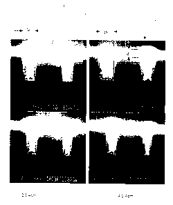
The coating result is illustrated in Fig. 1 with reference to cross
sections through the wafer 1, said wafer having recesses 2, which are filled
with copper 3 and have variable widths D prior to a CMP method being
carried out. The surfaces of the raised locations on the wafer 1 are also
coated with the copper layer 3. The copper layer thickness d over the
recesses 2 is surprisingly greater than over the raised locations on the wafer
1. In consequence, it is root very complex to achieve a flat surface of the
wafer 1 by the CMP method.