Note: Descriptions are shown in the official language in which they were submitted.
CA 02359548 2005-O1-14
v
COUPLING OF OPTICAL SIGNALS TO
MISALIGNED i~VAVEGUIDES ON DIFFERENT WAFERS
CROSS-REFERENCE TO RELATED APPLICATICINS
Related subject matter is disclosed in my previously filed application
entitled
"LARGE NxN OPTICAL StVITCH USING BINARY rCREES," Serial No. 09/653,449,
filed on October 11, 2000, issued on September 24, 2002 ay U.S. Patent No.
6,456,752, and
assigned to the same assignee.
TECHNICAL FIELD OF THE INVENTION
The present invention relates to the interconnection of optical waveguides
and,
more particularly, to a technique for the coupling of optical signals to
misaligned
io waveguides located on different wafers.
BACKGROUND OF THE INVENTION
In high capacity optical networks, an essential device is the N x N
crossconnect
switch. The function of this switch is to provide at each node full
connectivity among
several incoming fibers, each carrying several wavelength channels [1 - 6].
(Note in
this specification, a reference to another document is designated by a number
in
brackets to identify its location in a list of references found in the
Appendix In my
above identified related patent application, I described a technique for
implementing an
N x N crossbar switch by including orthogonal sets of planar switches directly
joined
together without fiber connections. This technique ca.n be used for the design
of a
2o N x N switch using the classical crossbar arrangement shown in Fig. I . The
basic
purpose of the N x N crossbar switch arrangement is to form a total of N2
paths
without waveguide crossings. In operation, a switch connection between N
inputs and
N outputs is realized by the arrangement by activating N particular paths,
while
blocking the remaining paths. The N2 paths are produced by two sets of planar
switches, arranged in input and output block arrays that are directly jointed
together,
with a rotation of ninety degrees between the two blocks as shown in Fig. I.
Each of
the N input switches is connected to all N output switches, and each of the N
output
CA 02359548 2001-10-22
CP Dragone 67 2
switches is connected to all N input switches. The input and output planar
arrays of N
switches are all identical, and they can be realized without waveguide
crossings in
integrated form.
A difficulty, with the above arrangement, is that it requires over the
junction
plane precise alignment between the input and output input an output arrays.
SUMMARY OF THE INVENTION
In accordance with the present invention, I have solved the above-described
difficulty by using adaptive imaging to minimize alignment errors in the
active paths.
The arrangement can also reduce crosstalk, since it can be designed to perform
as a
1o switching arrangement substantially reducing transmission in the crosstalk
paths.
In one embodiment, an N x N optical cross-connect is constructed using
orthogonal abutting of arrays of planar switches. If N is not too large, the
optimum
construction involves only two stages of planar switches, each incorporating
an adaptive
imaging arrangement allowing the input and output switches to be directly
joined
together without need for precise alignment.
My adaptive imaging arrangement technique may, more generally, be used to
align a first waveguide on a first wafer to a second waveguide on a second
wafer. In
general, misalignments occur both in the plane of the first wafer and in the
orthogonal
direction. Therefore effcient correction requires in general that the two
wafers be
2o approximately orthogonal to each other, and two adaptive imaging
arrangement are
required, one in each wafer. Thus, my adaptive imaging arrangement technique
may be
used to maximize coupling between waveguides located on different wafers or,
more
generally, between two arrays of waveguides located on two arrays of abutting
wafers.
The arrangement can also be designed to perform as a switching device, capable
of
maximizing transmission when it is traversed by an intended signal, and also
capable of
minimizing transmission when it is only traversed by a crosstalk path.
In accordance with my invention, I disclosed an apparatus for interconnection
of
two or more optical waveguides comprising
CA 02359548 2005-O1-14
3
a first planar wafer having a first optical imaging device for selectively
focusing a first signal on a first optical waveguide to a first focal point
located
along a predefined farst focal interval of an edge of the first wafer;
a second waveguide located on a second planar vaafer that has an abutting
edge forming an intersection junction with the edge of the first wafer, the
second
wafer includes an optical imaging device for selectively coupling a second
signal on
a second optical waveguide to a second focal point located along a predefined
second focal interval of the abutting edge of the second wafer, the focal
intervals of
the first and second wafers intersect each other; and
l0 wherein the first and second optical imaging devices each operate in
response to a control signal to align their respective focal points with the
intersection junction and thereby maximize signal coupling from the first
optical
waveguide to the second optical waveguide.
According to another aspect of my invention, the optical waveguide
interconnection apparatus may be arranged as an NxN optical cross-connect
apparatus comprising
a first plurality of first planar wafers, each first wafer including an input
optical waveguide connected to a IxN switch, each of the N output waveguides
of
the switch having an optical imaging device for selectively coupling said
first signal
to a focal point located along said predefined first interval of the abutting
edge of
the first wafer, thus forming a first array of disjoint intervals, each
corresponding to
a particular output waveguide of a particular first wafer;
a second plurality of second planar wafers, each second wafer including an
Nxl switch connected to an output optical waveguide, each of the N input
waveguides of the switch having an optical imaging device for selectively
coupling
the optical waveguide to an input focal point located along said second
predefined
interval of the abutting edge of said second wafer; thus forming a second
array of
disjoint intervals, each corresponding to a particular input waveguide of a
particular
second wafer;
CA 02359548 2005-O1-14
4
wherein the plurality of first and second wafers are essentially abutted
orthogonal to each other to form a grid of intersection junctions therebetween
and
wherein each interval of the first array intersect a corresponding interval of
the
second array; and
wherein each pair of optical imaging devices producing a pair of
intersecting intervals are responsive to a control signal to align their
respective focal
points to enable the coupling of an optical signal from a first optical
imaging device
to a second optical device of said pair.
According to another aspect of my invention., I disclose a method of operating
an apparatus for interconnecting optical waveguides comprising the steps of
abutting a first edge of a first planar wafer to a second edge of a second
planar wafer, the first wafer having a first optical imaging device for
selectively
coupling a first optical signal to a first focal point: located along a first
predefined
interval of the first abutting edge of the first wa~Per and the second planar
wafer
having a second optical imaging device for selectively coupling a second
optical
signal to a second focal point located along a second predefined interval of
the
second abutting edge of the second wafer so as to overlap said first
predefined
interval of the first abutting edge of the first wafer; and
selectively operating at least one of the first and second optical imaging
devices to enable the first focal point to align with the second focal point
to enable
optical signal coupling between the first optical imaging device and the
second
optical imaging device.
BRIEF DESCRIPTION OF THE DRAWINGS
In the drawings,
Fig. la shows a block diagram of an NxN crossbar switch implemented
using two orthogonal sets of planar switches.
Fig. 2 shows a first embodiment of an imaging arrangement of r = .~
waveguides.
Fig. 3 shows the arrangement of Fig. 2 realized by using an efficient
imaging arrangement of three waveguides combined with two radial arrays"
CA 02359548 2001-10-22
CP Dragone 67 5
Fig. 4 illustratively shows the calculated losses versus alignment
displacements
for an efficient imaging arrangement of Fig. 3 with r = 2, 3 .
Fig. 5 shows the alignment displacements 8x, 8Y at the junction of two
illustrative orthogonal planar switches of Fig. 1.
Fig. 6 shows two illustrative orthogonal planar switches of Fig. I utilizing
the
imaging arrangement of Fig. 3.
Fig. 7 shows an imaging arrangement of two slab sections with reflective
boundaries.
Fig. 8 shows calculated losses versus alignment displacements for the
to arrangement of Fig. 7.
In the following description, identical element designations in different
figures
represent identical elements. Additionally in the element designations, the
first digit
refers to the figure in which that element is first located (e.g., 102 is
first located in Fig.
1).
t5 DETAILED DESCRIPTION
In accordance with the present invention, I describe the construction of an
N x N optical cross-connect by using I xN and Nx I planar switches formed,
illustratively, using binary trees of 1 x2 and 2x 1 elements. If N is not too
large, the
optimum construction involves only two stages of trees, each incorporating an
adaptive
2o imaging arrangement allowing the input and output trees to be directly
joined together
without need for precise alignment. A similar construction is used for larger
N, by
including a larger number of stages. In all cases the arrangement features
minimum
loss and crosstalk. Note while thelxN and Nx 1 planar switches are described,
illustratively, as using binary trees of 1 x2 and 2x 1 elements, other known
types of I xN
25 and Nx I planar switches may also be utilized.
With reference to Fig. 1, this technique is described for use in the design of
a
N x N switch using the classical crossbar arrangement. The basic purpose of
the
N x N crossbar switch arrangement is to form a total of N2 paths without
waveguide
CA 02359548 2001-10-22
CP Dragone 67 6
crossings. In operation, a switch connection between N inputs, I1 - IN, and N
outputs,
O1 - ON, is realized by the arrangement by activating N particular switch
paths, while
blocking the remaining switch paths. The NZ paths are produced by two sets of
planar
switches, arranged in input 101 and output 102 block arrays that are directly
jointed
s together at a junction plane 103, with a rotation of ninety degrees between
the two
blocks as shown in Fig. 1. At junction plane 103, each of the N input switches
is
connected to all N output switches, and each of the IV output switches is
connected to all
N input switches. The input and output planar arrays of N switches are all
identical, and
they can be realized without waveguide crossings in integrated form. The input
I xN and
to output Nx I planar switches 105 and 106 are formed, respectively, using
binary trees of
1 x2 and 2x 1 elements without waveguide crossings. Each of the 1 x2 and 2x 1
elements
104 is separately controlled by a control signal (not shown). The input and
output
planar switch arrays are all identical, and they can be realized without
waveguide
crossings in integrated form. The absence of waveguide crossings simplifies
and
15 improves the design of each planar switch and N as large as 64 can be
realized, using
current technology, with negligible crosstalk and loss close to 5 dB.
The main difficulty with the Fig. 1 arrangement is that it requires, over the
junction plane 103, precise alignment between the input 101 and output 102
switch
arrays. In accordance with the present invention, in order to minimize
alignment errors,
2o I include in each path, in the vicinity of the junction plane 103, an
adaptive arrangement
performing variable imaging.
With reference to Fig. 2, the imaging arrangement 200 is shown to include an
optical signal splitter 201 connected by an array of waveguide paths 202 to an
imaging
section 203. The focusing section 203 produces at P a filtered image of the
mode
25 produced at Po by the input optical signal received over waveguide 210.
Each
waveguide path 202, except possibly for one particular waveguide, includes a
waveguide length adjuster 204 for controlling its respective waveguide length
under
control of a control signal 205. Since all waveguide length adjustments are
made
CA 02359548 2005-O1-14
7
relative to a particular reference waveguide, no waveguide length adjuster is
needed in
general on the reference waveguide. The reference waveguide when the number of
waveguides 202 is an odd number can be for instance the center waveguide, as
in Fig. 3.
If the number of waveguides 202 is an even number, then only one of the
waveguide
above or below the center position need not have a length adjuster 204. Thus,
if the
number of waveguides is r, then the number of waveguide adjusters is equal to
r-1.
Returning to the Fig. 2 example, by changing the length of the waveguides
above and below. the center waveguide in different directions, by a
predetermined
amount, the focus F of the output optical signal can be changed. These
waveguide
to adjustments are made by control signals 205, with the rcault that the focal
point location
P can be changed by an amount & in either direction from the normal focus
location F.
A control unit, not shown, stores the values of the control signals 205 needed
to provide
the correct adjustment to the waveguide adjusters 204 to be able to properly
position the
focus location F for all of the desired operating states of imaging
arrangement 200.
The imaging arrangement 200 is characterized by two principal operating
states,
respectively producing maximum and minimum transmission. Maximum optical
transmission (first state) is obtained by aligning the foal point P to the
receiving path
206, as in Fig. 2, and minimum transmission (second state) is obtained by
producing a
large displacement of the focal point P from the receiving path 206. Thus the
first state
is used by the arrangement to minimize alignment errors when the arrangement
is
traversed by an active path and, the second state, us used to block
transmission
when the arrangement is idle, and therefore it only receives crosstalk.
As noted, wavelength adjusters 204 can vary the optical path length difference
of the waveguides 202 forming the array. These wavelength adjusters 204
operate in a
well-known manner, for instance by using the optoelectric effect, or by local
temperature variation produced by a suitable heater. As a result the image
location can
be varied, and the width of this variation 8 is approximately (r -1)W where W
is the
image (401 of Fig.4) width and r is the number of waveguides.
CA 02359548 2001-10-22
CP Dragone 67 8
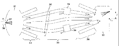
With reference to Fig. 3, the above imaging arrangement of Fig. 2 can be
realized efficiently by using two slabs 301, 302 connected by two radial
arrays 303, 304
of closely spaced waveguides (with spacing a and gap s) connected together by
waveguide arms 305 [7-9]. The input waveguide 306 is then located at the focal
point
307 of the first array 303 and the image is produced in the vicinity of the
focal point F
of the second array. The image displacement 8 from the focal point is
determined by
the optical path length difference of the r waveguides (303, 304, 305). A
similar
arrangement was used in references [7,8] to construct a wavelength router, by
using a
waveguides grating of non-zero order producing a wavelength dependent image
1o displacement. Here, however, the order must be zero since the displacement
must be
wavelength independent to a good approximation.
As in references [7,8], the purpose of the Fig. 3 imaging arrangement is to
transform the mode of the input waveguide into an output replica at the image
location
P displaced by b from the output focus F. In practice, the image is not an
exact replica
of the waveguide mode and this causes a mismatch loss, determined by the
coupling
coefficient between the actual image and the desired replica. The loss is
minimized, as
in reference [9], by optimizing the waveguide array 308, whose efficiency
approaches
unity if the number of waveguides r is large and they are closely spaced with
small
gaps, s, between their cores at the junction with the output slab 302. In our
present
2o application, however, it is important to minimize the number r -1 of
controls and we
therefore choose r = 2, 3 .
Fig. 4 shows typical calculated losses versus alignment displacements b for an
optimized imaging arrangement of Fig. 3 with r = 2, 3 . Fig. 4 also shows,
501, the
coupling loss variation for two waveguides displaced by 8, in microns. In this
case, the
largest b misalignment that can be tolerated by two waveguides without
exceeding a
loss of one dB is
8 = I .4 microns ( I )
whereas my imaging arrangement allows a much larger deviation,
CA 02359548 2005-O1-14
9
S = 3.7, 5.6, for r = 2, 3 . (2)
This increase in allowable deviation afforded by my imaging arrangement
substantially reduces the path alignment problem 8x, by shown in Fig. 5.
Fig. 5 shows the alignment displacements bx, 8y at the junction of two
illustrative orthogonal planar switches 500 and 501 of Fig. 1. In this
arrangement each
path is formed by a pair of orthogonal planes which must be . joined together
with
minimal displacements between the two waveguides 502 and 503 farming the path.
The coupling losses at the junction of two waveguides 502 and 503 in Fig. 5
are caused
by two orthogonal displacements 8 ~, 8y that must be corrected by using two
orthogonal
imaging arrangements. The total loss in Fig. 5 is therefore twice (we need two
arrangements) the loss (for one arrangement) in Fig. 4.
Shown in Fig. 6 are the two illustrative orthogonal planar switches 500 and
501
of Fig. 1 utilizing the imaging arrangement of Fig. 3. The imaging
arrangements are
shown, illustratively, by 601, 602 for the two waveguides 502 and 503,
respectively,
and shown in block form 603 and 604 for the other paths of planar switches 500
and
501, respectively.
Returning to Fig. 5. So far I have considered the loss through waveguides,
502 and 503, whose loss must be minimized. For all other paths, 505 and 506 of
planar switches 500 and 501, respectively, where no signal path is to be
established,
2o substantial loss is provided by the extinction ratios of the elements 104.
It is generally
desirable to increase this loss, and an important feature in Fig. 5 that a
substantial
increase is readily obtained by properly choosing the controls of the imaging
arrangements 603 and 604 so as to maximizes their loss. The only drawback is
an
increase in complexity of the control algorithm. The calculated increase in
extinction
2s ratio for paths 505 and 506, as provided by the imaging arrangements 603
and 604 of
Fig. 6, typically exceeds 20 dB for an optimized design. Also notice that
fabrication
errors will cause, in general, different losses in the N active paths in
Figure 1. lft may be
desirable to equalize these losses, or at least reduce the difference between
their
CA 02359548 2001-10-22
CP Dragone 67 10
maximum and minimum values, instead of minimizing the loss of each individual
path.
Clearly this can be realized by simply adjusting the controls of the active
paths that
have larger losses, so as to increase all losses that are lower than a
specified acceptable
loss.
With reference to Fig. 3, imaging section 302 primarily causes the above
losses.
These losses can be reduced as follows. Consider for simplicity r = 2 . The
loss of the
imaging section 302 is best derived by reversing transmission and determining
the
power transmitted to the r arms from a waveguide displaced by 8 from the
focus. The
loss for r = 2 consists of two components. One component arises because only
some of
1o the power is transferred to the two arms 701, 702 and, the other, because
the power is
not evenly transmitted to the two arms. Introducing reflective boundaries 704,
705 in
the imaging slab as in Fig. 7 can reduce both problems. The slab now consists
of a
uniform section 705 combined with a parabolic section 704. Some of the power
that in
the previous arrangement of Fig. 3 was lost is now redirected by the
reflective
boundaries 704, 705 towards the receiving waveguides 701, 702, and typical
results are
shown in Fig. 8. From a comparison with Fig. 4, one can see that the losses
are
substantially reduced. In particular, the previous loss of 1 dB for r = l, 8 =
3.7 to
about 0.5 dB.
Use of the above imaging arrangement technique in the N x N crossbar switch of
2o Fig. 1 both eliminates waveguides crossings and simplifies the realization
of each
planar switch since high extinction ratios are not any more required by switch
elements
104. This is because the imaging arrangement at each leaf of the 1 xN binary
tree 1 O 1 or
Nx 1 binary tree 102 provides a high (typically more than 20 dB) extinction
ratio.
Moreover, the waveguide bends can now be realized with large curvatures since
small
angles of rotation are not required, because of the absence of waveguides
crossings. A
consequence of this is that a small effective refractive index difference on
is generally
desirable to simplify fabrication and improve efficiency. For this reason a
value of
CA 02359548 2001-10-22
CP Dragone 67 11
4n l n = 0.0025 was assumed in the above example. The actual refractive index
difference is larger, about 0.004.
As previously noted, the imaging arrangement can be utilized in the
N X N crossbar optical switching arrangement described in my previously
referenced
patent application. Such a combination would offers advantages over the
arrangement
of reference [4]. The latter arrangement requires 2N stages and a total length
of about
66 cm for N =16 . The present arrangement, on the other hand, requires only
2log N
stages and it is characterized by lower loss and lower crosstalk. For
instance, for an
average loss per stage of less than 0.2 dB, the total loss will be primarily
caused by the
to junction loss, and it should be less than 5 dB for N as large as 64. The
largest N that can
be realized is determined by the spacing H (shown in Fig. 1 ) of the
rectangular array
formed by the waveguides on the junction plane. By choosing a spacing of 1 mm,
the
total width (N -1)H for N = 64 is 6.4 cm, easily fitting on a 6-inch wafer.
Notice in Fig. 3 that the required path length difference determined by b is
small, and it must be zero when the image is produced at the focal point F. In
order to
satisfy this condition the waveguide arrangement in Fig. 3 is composed of two
section
having opposite path length differences as in reference [10], and the net
result is zero
difference for 8 = 0 .
The above discussions were directed so far to the problem of directly joining,
2o without fiber interconnections, two orthogonal sets of planar wafers,
forming at their
junction an array of paths connecting each wafer to all other wafers (Fig. I
). Clearly as
also discussed above, my techniques also apply to the problem of connecting
together
two waveguides, formed on different wafers (e.g., Fig. 6). Additionally, my
techniques
also apply to the problem of directly joining a first wafer having N optical
imaging
devices to an orthogonal set of N second planar wafers, forming a linear array
junction
connecting, each of the N optical imaging devices of the first wafer to an
optical
imaging device on a different second wafer of the orthogonal set of N second
planar
wafers. This is shown in Fig. 1, where wafer 105 connects to each of the N
wafers of
CA 02359548 2001-10-22
CP Dragone 67 12
array 102. As shown in Fig. 1, my adaptive imaging arrangement technique is
used in
two orthogonal sets of N planar switch wafers that form an NxN crossbar
switch. It
should be understood, however, that each of the two orthogonal sets of N
planar wafers
need not be restricted to binary switch circuits but, more generally, the
planar wafers
may contain other types of optical circuits which have N optical waveguides
which have
to be interconnected. Moreover, each planar wafer of each set of N planar
wafers need
not all contain the same type of optical circuit but may, instead, contain
different types
of optical circuits. Thus, my adaptive imaging arrangement technique is not
limited to
switch applications, but more generally can be used for optical
interconnections
1o between single waveguides, linear arrays of waveguides, or two-dimensional
arrays of
waveguides.
In all the above-described applications, my adaptive imaging arrangement
technique can be used to minimize alignment errors. In general, these errors
occur both
in the plane of the first wafer and in the orthogonal direction. Therefore
efficient
correction requires in general that the two wafers be approximately orthogonal
to each
other, and two adaptive imaging arrangement are required, one in each in each
wafer.
CA 02359548 2001-10-22
CP Dragone 67 13
APPENDIX
REFERENCES
[1] Padmanabhan, K., and Netravali, A., ''Dilated Networks for Photonic
Switching,"
IEEE Transactions on Communications, Vol. COM-35, No. 12, pp. 1357-1365,
December 1987.
[2] Nishi, T., Yamamoto, T., and Kuroyanagi, S., "A Polarization-Controlled
Free-
Space Photonic Switch Based on a PI-Loss Switch," IEEE Photon. Technol. Lett.,
Vol. 6, No. 9, pp. 1104-1106, September 1993.
[3] Kondo, M., Takado, N, Komatsu, K., and Ohta, Y., "32 Switch Elements
1o Integrated Low Crosstalk LiNb03 4 X 4 Optical Matrix Switch," IOOC-ECOC 85,
Venice, pp. 361-364, 1985.
[4] Goh, T., Himeno, A., Okuno, M., Takahashi, H., and Hattori, K., "High-
Extinction
Ratio and Low Loss Silica-Based 8 x 8 Thermooptic Matrix Switch," IEEE
Photon. Technol. Lett., Vol. 10, No. 3, pp. 358-360, March 1998.
[5] Granestrand, P., Lagerstrom, B., Svensson, P., Olofsson, H., Falk, J. E.,
and Stoltz,
B., "Pigtailed Tree-structured 8 X 8 LiNb03 Switch Matrix with 112 Digital
Optical Switches," IEEE Photon. Technol. Lett., Vol. 6, pp. 71-73, 1994.
[6] Murphy, E. J., Murphy, T. O., Ambrose, A. F., Irvin, R. W., Lee, B. H.,
Peng, P.,
Richards, G. W., and Yorinks, A., " 16 x 16 Strictly Nonblocking Guided-wave
2o Optical Switching System," J/Lightwave Technol., Vol. 10, pp. 810-812,
1998.
(7] Dragone, C., "An Optical Multiplexer Using a Planar Arrangement of Two
Star
Couplers" IEEE Photon. Technol. Lett. 3, pp. 812-815, 1991.
[8] Dragone, C., Edwards, C., and Kistler, R. C., "Integrated Optics N X N
Multiplexer on Silicon," IEEE Photon. Technol. Lett. 3, pp. 896-899, 1991.
(9] Dragone, C., "An N X N Optical Multiplexer Using a Planar Arrangement of
Two
Star Couplers," IEEE Photon. Technol. Lett., 3, pp. 812-815, 1991.
[IO] Adar, R., Dragone, C., and Henry, C. H., "Planar Lens and Low Order Array
Multiplexer," U.S. Patent 5,212,758.