Note: Descriptions are shown in the official language in which they were submitted.
15-03-2001 CA 02360317 2001-07-13 ES 009900382
= 1
HIGH VOLTAGE TRANSFORMER
OBJECT OF THE INVSNTION
The invention that is being dealt with consists in a high
voltage transformer the goal of which is to considerably
reduce the size and the price thereof.
Obviously, the invention can be used in all those
applications where a h'igh .kilovoltage supply is being
required, both in direct and in high or low frequency
alternate current.
SAAC~tOO~D OF Tn IliV811TIM
Conventionally, the use of high kilovoltage
transformers the design of which presents a maximum
difficulty in achieving the electrical insulation between
the various elements (transformers, high voltage switches,
rectifiers, voltage dividers, dischargers, etc.) they are
composed of, is more than known. Insulation thereof is
conventionally made by three different manners:
1. Filling, at vacuum and in a dry environment, the
whole inside of the tank or housing containing the various
elements of the transformer with a liquid or gaseous fluid
which is usually silicone oil or mineral oil due to the
low cost thereof.
2. Using solid insulating parts as there are
plastics, glasses, porcelains, resins, etc.
3. Vacuum encapsulating the whole assembly with
high voltage insulating silicones or resins.
In any of these three manners of making the
insulation, it is necessary to keep some minimum distances
between the various elements composing the transformer.
This minimum distance depends on the voltage applied
between the various elements so that it is necessary to
keep a minimum insulation distance between the points of
major voltage, which involves in the majority of the
cases, the insulation distance becomes excessive for
achieving insulation between the points of minor voltage.
AMENDED SHEET
=:, 15-03-2001 CA 02360317 2001-07-13 ES 009900382
2
The final consequence is that the elements occupy a very
high volume, whereby this volume must moreover be covered
with the insulating material, a fact which considerably
increases the weight and, especially, increases the cost
of the transformer.
Furthermore, this design for achieving minimum
distances, renders the assembly of the various elements of
the transformer difficult, a fact which equally increases
its cost.
The United States patent 4,587,606 describes a
secondary winding divided into a plurality of sections
provided around a primary winding of the air-core type.
First and second diode groups are disposed on four
substrates which surround the secondary winding. Diodes in
each of the first and second diode groups are disposed on
two adjacent substrates so that these diodes are connected
in series so as to have the same polarity direction,
respectively.
The first and second diode groups are respectively
divided into a plurality of diode sections. winding start
ends and winding finishing ends are coupled between the
respective two adjacent diode sections.
The diode sections disposed on each substrate are
arranged to be spaced apart along the axial direction of
the primary winding. One of the diode sections to which
induced voltages of the winding sections are applied is
disposed on two adjacent substrates, and the other diode
section is disposed on the other two adjacent substrates.
Positions of these diode sections are shifted along the
axial direction of the primary winding. Therefore, the
diode sections to which the induced voltages of the
winding sections are applied are disposed on different
substrates and are not on the same plane.
The Japanese patent application 6333754 A describes a
transformer for cycloconverter to provide a transformer
=
AMENDED SHEET
,,15-03-2001 CA 02360317 2001-07-13 ES 009900382
3
with equal factors of resistance and leakage reactance in
positive and negative groups of windings.
In a first constitution, a conductor,in a positive
group winding and a conductor in a negative group winding
are turned double in an axial direction on a core leg at
the same time.
In a second constitution, the positive group.winding
and the negative group winding are put on separate
divisions in an axial direction of the=core leg. Then, a
power-supply winding is split into two and they are
mounted around each outer boundary of the positive and
negative group windings.
DESCRIPTION OF THE IDVSNTION
To solve the afore indicated inconveniences, the
invention has developed a new high voltage transformer
which is characterized in that the conventional elements
it is constituted of are arranged in two differentiated
groups, on the one hand the elements having positive
voltage and, on the other, the elements having negative
voltages, both groups being separated by insulating means.
Furthermore, the arrangement of the elements provides
that they are advantageously designed in such a manner
that one of the ends of all thereof, have ground level or
"zero" voltage. This voltage progressively increases
towards the opposed end in the elements having positive
voltages, and progressively decreases in the elements
having negative voltages; all this in such a manner that,
at an equal distance from ground level, the elements of
each group have equipotential voltages.
This structure has the great advantage that the
elements of one same group do not need insulation between
themselves, so that the distance which is to separate them
is considerably reduced, and, furthermore, the elements
occupying the same area of potential do not at all have an
influence on the stray capacitance, so that there are no
AMENDED SHEET
15-03-2001 CA 02360317 2001-07-13 ES 009900382
4
limitations neither in respect of their proximity nor in
respect of the opposed surfaces between them.
Thus, by means of the invention, as the elements are
designed such that their voltage levels are in accordance
with the area of potential which they occupy, it is
possible to bring the elements nearer to each other, so
that the volume is considerably reduced and, thus, the
insulator filling the inside of the housing or tank of the
transformer, is considerably reduced.
As a consequence of this reduction of the volume, a
considerable reduction of the weight is achieved, due to
the fact that the tank is of smaller dimensions and a
smaller quantity of filling insulator is required.
Another of the advantages of the present invention is
the reduction of the stray capacitance which eliminates
some undesirable side effects.
The progressive increase of the voltage in the
elements having a positive voltage, and the progressive
decrease of the voltage in the elements having a negative
voltage, are linear.
Advantageously, the ground level or "zero voltage",
is located in the area where the low voltage input signals
are located.
In a preferred embodiment, the "zero voltage" level
is located on the upper side of the transformer, such that
the maximum level of potential is defined at the lower
ends of the high voltage switches.
The insulating means separating the two groups of
elements, are established by one single solid insulating
means, a fact which considerably simplifies the assembly
of the various elements of the transformer at the same
time as it reduces its cost.
Another feature of the invention resides in the fact
that it has means for minimizing the stray capacitance
between the elements of one group and the elements of the
AMENDED SHEET
CA 02360317 2006-09-27
other. These means are determined by the arrangement
presented by the various elements of one group and the
other; said elements are located in such a way that the
surface of the elements cf one group opposed to the
surface of the elements of the other group, is minimum.
By means of the invention, the number of supporting
and electrical insulation parts as well as manpower needed
for assembling is reduced.
As a consequence of the above, it is evident that the
invention considerably reduces the total-cost of the tank,
as well as that of the storage and transport thereof.-
Hereafter, so as to facilitate a better-understanding
of this description and forming an integral part thereof,
a series of figures in which the object of the invention
is represented in an illustrative, non-limiting way; is
attached hereto.
According to an aspect of the present invention there
is provided a high voltage transformer having a plurality
of elements for voltage transformers, the elements
comprising: high voltage transforming means, rectifiers,
filters, resistive dividers, high voltage switches,
magnetic cores, and a low voltage input, wherein each
rectifier, filter, resistive divider, high voltage switch,
magnetic core, has a first end and a second end, each first
end being connected to zero voltage level, each second end
being opposite to each first end, the rectifiers, filters,
resistive dividers, high voltage switches, magnetic cores,
being arranged in two differentiated groups, a first group
comprising positive voltage elements and a second group
comprising negative voltage elements, the positive voltage
elements are separated from the negative voltage elements
by solid insulating means in two insulated chambers,
CA 02360317 2006-09-27
5a
voltage towards the second end in each of the elements
progressively increases in the positive voltage elements
and, progressively decreases in the negative voltage
elements, so that, at an equal distance from the zero
voltage level, the elements of each group have
equipotential voltages.
BRZEF DESCRIPTION OF THE DRAWINGS
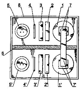
Figure 1 shows a schematic top plan view of a
possible embodiment of the transformer of the invention.
In this figure the upper surface or cover of the housing
or tank of the transformer has been removed.
Figure 2 shows a side view of the transformer shown
in the preceding figure, in which the lateral surface has
been removed so as to clearly appreciate the arrangement
of the various elements.
Figure 3 shows a view in accordance with section A-B
of the preceding figure.
DESCRIPTION OF A PREFERRED EMBODIMENT OF TAE IM!ENTION
Hereinafter, a description of the invention will be
made on the basis of the aforementioned figures.
The transformer of the invention presents as a
characteristic the fact that the conventional elements it
is comprised of, are arranged in two differentiated
groups, in such a manner that, on one side, there are
situated the elements with positive voltages and, on the
15-03-2001 CA 02360317 2001-07-13 ES 009900382
6
other, the elements with negative voltages.
For this purpose, in a longitudinal half of the
transformer there are arranged: a high voltage transformer
1 with its magnetic core 7, a rectifier 2, a filter 3, a
resistive divider 4 and an anode switch 5 which constitute
the elements supporting positive voltages.
In the other longitudinal half there are arranged, a
high voltage transformer 1' with its magnetic core 7', a
rectifier 2', a filter 3', a resistive divider 4', and the
cathode switch 5' which constitute the elements supporting
negative voltages.
Between both groups, there is arranged a solid
insulating means (6) furnishing correct insulation between
the two groups, whereas insulation between the various
elements of each group is achieved by means of a fixing to
a "zero voltage" or ground level on the upper side, which
is progressively increased towards the lower end in the
elements with positive voltage and which progressively
decreases in the elements with negative voltages, in such
a way that at one same distance from ground level, the
elements of each group have equal voltages as represented
in figures 2 and 3 wherein voltage.levels of 0+ 20kV, +
40kV, 80kV have been marked.
Hereby, the potential becomes linearly increased as
from the level of 0 Volt downwards, whereby the maximum
level of potential is defined. by the lower ends of the
switches 5 and 5'.
Achievement of equipotential levels permits the
elements occupying the same level of potential to be
brought near to each other until almost contacting each
other, as they do not need insulators and do not at all
have an influence on the stray capacitance, and there are
thus no limitations neither in respect of their proximity
nor in respect of the opposed surfaces therebetween, so
that the total volume of the transformer is considerably
AMENDED SHEET
15-03-2001 CA 02360317 2001-07-13 ES 009900382
7
reduced.
Furthermore, as can be appreciated in figure 1, the
surface of the elements of one group being opposed to the
opposite surface of the elements of the other group, is
minimum, such that the stray capacitances are minimized.
All described elements remain included in housing 8
which is closed at its upside by cover 9 constituting the
point of zero voltage wherein low voltage input 10 is
arranged. Said low voltage input is negligible when
compared to the high voltage being generated. at the
various levels, and can therefore be considered as zero
voltage level.
As has been described before in chapter Background of
the Invention, the'inside of the tank or housing 8 is
filled with an insulating material which in the embodiment
is silicone oil or mineral oil, and as a matter of example
it may be pointed out that the amount of this insulator
needed for filling the whole of the volume, is of 4 liters
which in comparison to the 36 liters needed by
conventional transformers, ' represents a very high
reduction in volume with the subsequent saving represented
thereby.
Obviously, as already stated in chapter Background of
the Invention, the insulator being used can be
materialized by means of vacuum encapsulating the whole of.
the assembly with high voltage insulating silicones or
resins.
35
AMENDED SHEET