Note: Descriptions are shown in the official language in which they were submitted.
CA 02360836 2001-07-11
WO 00/42744 PCT/GB00/00161
Interface
The present invention relates to an interface between base band circuitry and
radio frequency transceiver circuitry, particularly circuitry operating in
accordance with the Bluetooth Low Power Radio Frequency Specification. It
additionally relates to devices having such an interface and either type of
circuitry.
Low power radio frequency systems allow communication between devices
over short distances typically ten's of meters. The devices must each be
capable of receiving and transmitting according to the system's protocol.
One low power radio frequency system is the Bluetooth system. This system
is designed to replace connecting wires and cables with wireless connectivity.
For one device to communicate with another device, no wires connecting
them will be necessary. Instead, each device will host a transceiver. A
transceiver has a baseband part and an RF part. The host itself may have
processing circuitry which is capable of doing the base band processing and
that host will only require RF transceiver circuitry to be correctly connected
to
that processing circuitry.
It would be desirable to create RF transceiver circuitry that can be connected
to many different hosts to provide the hosts with wireless connectivity.
It would be desirable to standardize the interface at which the connection
between the base band circuitry and the transceiver circuitry is made making
it vendor and platform independent.
CA 02360836 2001-07-11
WO 00/42744 PCT/GB00/00161
2
It would be desirable to have a simple interface between the baseband part
and the radio frequency part and in particular to have a reduced number of
pins in the interface. A reduced number of pins provides the advantages of
reduced chip area and reduced power consumption due to less toggling of
pins.
According to one aspect of the present invention there is provided a device as
claimed in claim 1.
According to another aspect of the invention there is provided transceiver
circuitry as claimed in claim 21.
According to further aspects of the invention there is provided a method
according to any one of claims 25 and 26.
According to a still further aspect of the invention there is provided an
interface as claimed in claim 27.
Embodiments of the present invention therefore provide an interface with a
low pin count and attendant low power consumption.
The low pin count arises out of: the burst mode controller and the
microcontroller both using the DBus; the burst mode controller using the DBus
for different tasks and the function of the RFBus being dependent upon the
operational mode.
The burst mode controller controls time critical tasks in the RF circuitry
using
the DBus and RFBus. The DBus is used to control time critical configurations.
The RFBus is used to transfer data and, in the transmit mode, to control the
power amplifier.
CA 02360836 2001-07-11
WO 00/42744 PCT/GB00/00161
3
For a better understanding of the present invention and to understand how
the same may be brought into effect reference will now be made, by way of
example only, to the accompanying tables and figures in which:
Table 1 illustrates the signals provided at the interface between Baseband
(BB) circuitry and Radio Frequency (RF) circuitry;
Table 2 illustrates the effect of operational modes on the signals provided at
the interface via RFBus;
Figure 1 a illustrates the BB side of the RF-BB interface;
Figure 1 b illustrates the RF side of the RF-BB interface;
Figure 1 c is a schematic illustration of a LPRF transceiver illustrating the
functionality of RFBus;
Figure 2a illustrates how RFBus is configured and how the RF chip responds
in the control mode;
Figure 2b illustrates how RFBus is configured and how the RF chip responds
in the transmit mode;
Figure 2c illustrates how RFBus is configured and how the RF chip responds
in the receive mode;
Figure 3 illustrates how the DBus may control devices in addition to an LPRF
RF chip having RF circuitry;
Figure 4a illustrates Write Access on DBus;
Figure 4b illustrates Read Access on DBus.
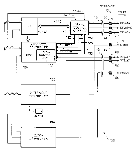
Figure 1 a illustrates baseband (BB) circuitry 100 having an interface 10. The
interface is connected or connectable to a similar corresponding interface 10
of radio frequency (RF) circuitry 200 illustrated in Figure 1 b.
The interface 10 has seven pins. The pins 20, 22 and 24 are assigned to the
bus of control signals DBus 12 and respectively transfer the signals DBusDa,
DBusEnX and DBusClk. The pin 30 is assigned to the sleep control signal
CA 02360836 2001-07-11
WO 00/42744 PCT/GB00/00161
4
SIeepX 14 . The pins 40, 42 and 44 are assigned to the bus of data signals
RFBus 16 and respectively transfer the signals RFBus1, RFBus2 and BBCIk.
The pins of the interface 10 in the BB circuitry connect or are connectable to
corresponding pins of the interface 10 of the RF circuitry 200.
The DBus 12 has three signal lines associated with the pins 20, 22 and 24. A
bi-directional signal line for transferring data signal DBusDa either from BB
circuitry 100 to RF circuitry 200 or from RF circuitry 200 to BB circuitry
100,
via pin 20. A unidirectional signal line for transferring an enable signal
DBusEnX from the BB circuitry 100 to RF circuitry 200, via pin 22. A
unidirectional signal line for transferring a clock signal DBusClk from the BB
circuitry 100 to RF circuitry 200, via pin 24.
The RFBus 16 has three signal lines associated with the pins 40, 42 and 44.
A bi-directional signal line for transferring signal RFBus1 via pin 40. A
unidirectional signal line for transferring a clock signal BBCLK from the RF
circuitry 200 to BB circuitry 100 via pin 44. A unidirectional signal line for
transferring signal RFBus2 from BB circuitry 100 to RF circuitry 200 via pin
42.
SIeepX 14 is a unidirectional signal line for transferring from the BB
circuitry
100 a signal SIeepX for controlling power-down in the RF circuitry 200.
Table 1 illustrates the signals provided at the interface 10 and identifies
each
one of the interface signals by their associated interface pin, their name,
their
direction and their function.
DBus
DBus 12 is a serial I/O Data Bus. It is a Clock, Data, Enable serial
interface.
It is not dedicated purely to the interface 10 between the RF circuitry 200
and
the BB circuitry 200. Figure 3, illustrates the situation in which the BB
circuitry
CA 02360836 2001-07-11
WO 00/42744 PCT/GB00/00161
100 is integrated into another host system. The BB circuitry 100 is the DBus
Master. In this example the host system is a radio telephone 300, but it could
be a computer or personal digital assistant (PDA). The DBus 12
communicates with DBus Slaves. One DBus Slave is the RF circuitry 200
5 which is connected to DBus via the interface 10. Other slaves communicated
with are in the example illustrated Power Supply Management Circuitry 310
and RF Modulator Circuitry 320 for the GSM protocol.
The DBus (DBusDa, DBusEnX and DBusClk) is used to control the RF
circuitry and other devices as illustrated in Figure 4. The DBus writes
control
data to and reads control data from registers in the RF circuitry 200. The
registers written to may include a register which controls the frequency at
which the RF chip transmits or receives, a register which controls the power
at
which the RF chip transmits and registers which identify whether the RF chip
is in the control, transmit or receive mode. The registers read from may
include a register containing RSSI information. Thus the DBus may control the
operation of the RF circuitry, for example, controlling the transition from
receiving to transmitting.
The BB circuitry 100 controls access to the DBus. The BB circuitry precedes
transferred data words with a device address, a Read/Write (R/W)
identification bit and a register address. Each device address is 3 bits long
allowing for 8 devices (the RF circuitry 200 and 7 others) to be accessed. The
R/W bit when LOW indicates the BB circuitry is to write to the addressed
register and when HIGH indicates that the BB circuitry is to read from the
addressed register. The register address is 5 bits long allowing 32 registers
to
be addressed. The data words may be of variable length and may have a
practical limit of 32 bits. Data words of 16 bits are preferred for transfer
to/from the RF circuitry 200.
CA 02360836 2001-07-11
WO 00/42744 PCT/GB00/00161
6
Address bits and R/W bit are verified before latching data to permit bus
sharing with devices which are used concurrently to RF circuitry 200.
Access via DBus is enabled by taking DBusEnX LOW half a clock cycle
before the first positive clock edge of DBusClk. At the first rising edge of
DBusClk the MSB of the device address will be clocked from DBusDa into the
DBus Slave.
A write access is illustrated in Figure 4b. To write to RF circuitry 200 the
DBus
Master circuitry 100 places data onto DBusDa at the falling edge of DBusClk.
The DBus Slave 200 having verified that it is addressed takes data from
DBusDa on each of the rising edges of DBusClk. The DBus Master 100
changes the state of data at the falling edge of each clock pulse of DBusClk.
Following the 8 address bits and R/W bit, data bits are sent with the same
timing as the address bits. Following the last data bit the enable line
DBusEnX
is taken HIGH. The clock then pulses one more pulse and is then held LOW
for a minimum of one cycle before a new access may be started. The enable
DBusEnX is therefore held HIGH for a minimum of two cycles.
A read access is illustrated in Figure 4a. The DBus Slave when being read
from, places data onto DBusDa on each of the rising edges of DBusClk. The
data is read from DBusDa by the DBus Master 100 on each of the falling edge
of DBusClk. During a read access the addressed device generates data on
the DBus to be read by the controlling device. Following the 8 address bits
and R/W bit there is a turn around bit which lasts for half a clock cycle and
has the effect of realigning the DBus timing such that the addressed device
will load bits onto the DBus upon the rising edge of the DBusClk. The bits are
read at the DBus Master 100 on the falling edges of the DBusClk. Following
the last data bit the DBusClk is disabled for at least one clock cycle before
the
next access. The data word length is not fixed. The DBus Master 100 controls
CA 02360836 2001-07-11
WO 00/42744 PCT/GB00/00161
7
DBusEnX. The number of data bits and the data word length is fixed for a
certain address by convention.
RFBus
The interface 10 has a dedicated pin for signal RFBus1, a dedicated pin for
signal RFBus2; and a dedicated pin for clock signal BBCIk (13MHz), used to
synchronize data transferred via RFBus. BBCIk may also be used for
clocking logic of BB circuitry 100. BBCIk is generated by RF circuitry 200 at
13MHz for symbol rate of 1 Mbaud @ 13 fold oversampling.
The RFBus 16 is multifunctional. RFBus is used for transferring received data
from the RF circuitry 200 to the BB circuitry 100, transferring data for
transmission from the BB circuitry 100 to the RF circuitry 200 and
transferring
control data between the BB circuitry 100 and RF circuitry 200. The ability of
the RFBus to transfer control data is used for different purposes depending
upon the operational mode of the system.
RFBus 1 is bi-directional. In a Transmit mode the RFBus 1 provides data to
the RF circuitry 200 for transmission. In a Receive Mode RFBus 2 receives
data from the RF circuitry 200. Although in the examples given a single data
signal RFBus1 is illustrated a plurality of such data signals may be used to
increase bandwidth.
RFBus 2 is used to control time critical tasks in the RF circuitry 200. Time
critical tasks are tasks which need to be effected on a time scale of less
than
1 bit width ( 1 ~,s in Bluetooth). RFBus2 is fast (13 MHz) at transmitting
control
signals from the BB circuitry 100 to the RF circuitry 200. In the Transmit
mode, RFBus2 is used to control the timing of the Power Amplifier. In the
Receive Mode RFBus 2 is used to control the timing of the DC estimator
changing from a fast data acquisition mode to a slower data acquisition mode.
CA 02360836 2001-07-11
WO 00/42744 PCT/GB00/00161
8
The operational mode of the system is determined by the BB circuitry 100.
The BB circuitry indicates a change of mode to the RF circuitry 200 via DBus.
The modes include Transmit Mode, Receive Mode and Control Mode.
Interface of BB circuitry
The BB circuitry illustrated in Figure 1 a has the interface 10 previously
described, it additionally has a Serial Control Interface 110, a Burst Mode
Controller (BMC) including a Timing Control Unit 130, a microcontroller 140, a
sleep mode controller 150 and clock distribution circuitry (CDC) 160. The
Serial Control Interface 110 provides DBus at pins 20, 22 and 24. The Burst
Mode Controller 120 provides RFBus1 at pin 40 and RFBus2 at pin 42. The
Sleep Mode Controller provides SIeepX at pin 30. The Clock Distribution
Circuitry 160 is connected to pin 44 of interface 10 and receives BBCIk from
the RF circuitry 200.
The CDC 160 provides clock signals derived from BBCIk to the BMC 120, the
microcontroller 140 and the Serial Control Interface 110.
The Serial Control Interface 110 is controlled to produce DBus by either the
microcontroller 140 or the Burst Mode Controller 120. The Burst Mode
Controller controls DBus when time critical configurations to RF circuitry 200
are made. Whether the microcontroller 140 or the BMC 120 controls the
content of DBus is determined by a switch signal 142 provided by the
microcontroller 140 to the Serial Control Interface 110. The BMC 120
provides Data information 122, address information 124 and R/W information
126 to the Serial Control Interface 110 which places this information in the
correct serial format on DBusDa. The clock signal DBusClk (13MHz) is
received from Clock Distribution Circuitry. The timing of the transitions in
the
CA 02360836 2001-07-11
WO 00/42744 PCT/GB00/00161
9
Enable signal DBusEnX are controlled by a Trigger signal 132 provided by the
Timing Control Unit 130 in the BMC 120.
The Burst Mode Controller 120 controls the content of RFBus1 and RFBus2
and may additionally control the content of DBus. It directly provides RFBus2
to pin 42 and provides RFBus1 to pin 40 in the Transmit Mode and receives
RFBus1 from pin 40 in the Receive Mode.
The microcontroller may access the DBus and hence the RF circuitry via the
Serial Control Interface. When the DBus is controlled by the microcontroller
no time critical tasks can be controlled via the DBus. This configuration is
used in the boot phase or for RSSI measurement. When the BMC 120
controls the DBus, it is possible to control time critical tasks via the DBus.
The
ability of the BMC 120 to control time critical tasks via the DBus depends
upon the resolution of the trigger signal 132 which is at least 1 ~.s. The
control
signals sent by the BMC 120 via RFBus2 may have an even higher resolution
if they are directly clocked by BBCIk @ 13MHz.
Interface of RF circuitry
Fig 1 b illustrates the RF circuitry 200 which has an interface 10. The
interface
has pins 20, 22 and 24 dedicated respectively to DBusDa, DBusEnX and
DBusClk, pin 30 dedicated to SleepX and pins 40, 42 and 44 respectively
dedicated to RFBus1, RFBus2 and BBCIk. The RF circuitry 200 includes a
Control Interface 210; a register set 220 illustratively including registers
222,
224 and 226; decoding circuitry 230; a NOT gate 232; a two input AND gate
234; a three input OR gate 236; power-supply regulator circuitry 240; a
reference oscillator 250; switching circuitry 260; Transmission Path 270 and
Reception Path 280.
CA 02360836 2001-07-11
WO 00/42744 PCT/GB00/00161
The Control Interface 210 has an input interface 212 connected to DBus and
a input 214 for receiving Sleep X. It has an output 216 for supplying a mode
control signal to the input of decoding circuitry 230 and to the control input
262 of the switching circuitry 260 and an interface 218 for accessing the set
of
5 registers 220. The Control Interface 210 receives DBus and performs the
appropriate action which may involve writing to a register or reading from a
register and changing the mode of operation of the RF circuitry 200. By
writing
to appropriate registers the Control Interface 210 may control the operational
mode of the RF circuitry 200, control the synthesizer frequency in the Tx or
Rx
10 path, control whether the RF circuitry should receive or transmit, and
control
the power at which the Tx path 270 should transmit. By reading from
appropriate registers information concerning received signal quality such as
RSSI can sent by the Control Interface 210 to the BB circuitry 100. For
simplicity of illustration the operative connections of the Rx Path 280 and Tx
Path 210 to the register set 220 are not shown. A two bit signal is provided
at
the output 216 indicating the operational mode- [10] indicates Receive Mode,
[01] indicates Transmit Mode and [11] indicates Control Mode.
The switching circuitry 260 has an input 262 connected to output 216 of the
Control Interface 210, a single primary interface and three secondary
interfaces. The primary interface has one port connected to pin 40 to transfer
RFBus1 and another port connected to pin 42 to transfer RFBus2. One of the
secondary interfaces is connected at any one time to the primary interface in
dependence on the signal received at the input 262. When the signal at input
262 indicates Control Mode a port 264 of a first one of the secondary
interfaces is connected to pin 40 via the switching circuitry 260. The port
264
is connected to one input of the AND gate 234. When the signal at input 262
indicates Transmit Mode a port 266 of a different one of the secondary
interfaces is connected to pin 40 via the switching circuitry 260 and the
other
port 267 of that secondary interface is connected to pin 42 via the switching
CA 02360836 2001-07-11
WO 00/42744 PCT/GB00/00161
11
circuitry 260. When the signal at input 262 indicates Receive Mode a port 268
of another of the secondary interfaces is connected to pin 40 via the
switching
circuitry 260 and the other port 269 of that secondary interface is connected
to pin 42 via the switching circuitry 260. The ports 266 and 267 and 268 and
269 are connected to the Tx Path 270 and Rx Path 280 respectively as further
illustrated in Figure 1 c.
The decoding circuitry 230 has a 2 bit wide input connected to the output 216
of the Control Interface 210 and provides its output to one input of AND gate
234 and, via NOT gate 232, to one input of OR gate 236. The decoding
circuitry 230 produces a HIGH output when the signal received at its input
identifies the Control Mode and a LOW signal otherwise.
The OR gate receives one input via the NOT gate 232 as described, another
input from the pin 30 which receives SIeepX and a final input from the output
of AND gate 234. The output of the OR gate 236 is provided as a standby
control signal to the Power-Supply Regulation Circuitry 240 and to the
Reference Oscillator 250. A LOW output from the OR gate 236 places Power-
Supply Regulation Circuitry 240 into a low power consumption standby state
and switches the Reference Oscillator 250 off.
The Reference Oscillator 250 provides its output to the pin 44. It's output is
also used elsewhere within the RF circuitry, but this is not illustrated for
purposes of clarity.
Figure 1c illustrates the control effected on the Tx path 270 during Transmit
Mode and the control effected on the Rx Path 280 during Receive Mode.
The Transmit path 270 includes Pulse Shaping Circuitry 272 which receives
an input from port 266 of switching circuitry 260 in the Transmit Mode and
CA 02360836 2001-07-11
WO 00/42744 PCT/GB00/00161
12
otherwise does not receive an input. The output of the Pulse Shaping Circuitry
272 is provided as an input to Modulation Circuitry 274 which provides the
modulated signal to Power Amplifier 276 for amplification and subsequent
transmission via an antenna. The power Amplifier 276 has a control input by
which the amplifier gain may be forced to ramp up or ramp down. This control
input is connected to port 267 of the switching circuitry 260. The power
amplifier can therefore be switched on or off.
The Receive Path 280 includes Frequency Down Conversion Circuitry 286
which receives an input from the antenna in the Receive Mode. The circuitry
286 converts the received signal to a lower frequency and provides it to
Demodulation Circuitry 284. The demodulated signal is provided to DC
estimation circuitry 282. The amplitude decided data output by DC Estimation
circuitry 282 is supplied to the port 268 of the switching circuitry 260. The
DC
Estimation Circuitry 282 has a control input connected to the port 269 of
switching circuitry 260. The signals provided at the control input determine
whether the DC Estimation operates in a fast mode or a slow mode.
Operational Modes
In the Transmit Mode, as illustrated in Figure 2b, RFBus1 and RFBus2 are
driven by BB circuitry 100. RFBus1 supplies digital data for transmission
<TXDATA> from BB circuitry 100 to RF circuitry 200 via pin 40. Logic levels
are used and pulse shaping is done completely in RF circuitry 200. RFBus2
controls the timing of powering up the Power Amplifier (PA) in the RF
circuitry
200 using control signal <PAON>. When RFBus2=<PAON>=HIGH the Power
Amplifier is on when RFBus2=<PAON>=LOW the Power Amplifier is off. The
switching on and off of the Power Amplifier is 'time critical' as it must be
controlled over time scales of less than 1 bit duration (1 ~s for Bluetooth
Specification 1.0 ).
CA 02360836 2001-07-11
WO 00/42744 PCT/GB00/00161
13
In Receive Mode, as illustrated in Figure 2c, RFBus1 is driven by RF circuitry
200 and RFBus2 driven by BB circuitry 100. RFBus1 supplies received data
<RXDATA> to the BB circuitry 100 via pin 40. RFBus2 controls DC estimation
in RF circuitry 200 via pin 42. The switching of DC estimation is 'time
critical'
as it occurs on a time scale of less than 1 slot duration. <DCTRACK>=LOW
cause use of a fast acquisition of a DC estimate which is typically used at
the
start of a received packet and <DCTRACK>=HIGH controls use of a slower
DC estimation which is typically used for the remainder of the packet. The
change of DC estimation is 'time critical' as it must be controlled over time
scales of less than 1 bit duration (1 ~s for Bluetooth Specification 1.0 ).
The Control Mode is the neutral mode entered when neither the Transmit
Mode or Receive Mode are active. It is entered when SIeepX is LOW or via a
control word on DBus. In this mode, as illustrated in Figure 2a, RFBus1 and
RFBus2 are driven by BB circuitry 100: RFBus2 does not have an assigned
functionality; RFBus1= <CIkOn>. When RFBus1=<CIkOn>=HIGH, AND gate
234 switches ON the Reference Oscillator 250 and the Power Supply
Regulation Circuitry 240. When RFBus1=<CIkOn>=LOW, AND gate 234
switches OFF the Reference Oscillator 250 and the Power Supply Regulation
Circuitry 240 into standby. The RF circuitry is placed in a low power mode.
There is no activity on DBus and RFBus and BBCIk is switched off.
It will therefore be appreciated that the RFBus is used for different purposes
during different operational modes of the system, as illustrated in Figures
2a,
2b, and 2c and Table 2.
The operation of a LPRF device is described in detail in UK Patent Application
No 9820859.8 , the contents of which are hereby incorporated by reference.
In particular Figure 4 shows LPRF RF components of a transceiver (Tx, Rx
CA 02360836 2001-07-11
WO 00/42744 PCT/GB00/00161
14
and Frequency control), connected to baseband components (the remaining
elements in the Figure).
In the preceding described embodiment, the receive path 280 was partitioned
so that the DC Estimation circuitry 282 was in the RF Circuitry 200. This
results in RFBus1, during the receive mode, transferring RxData from the RF
Circuitry 200 to the BB circuitry 100 across interface 10 and RFBus2
transferring a control signal, DcTrack, from the BB circuitry 100 to RF
Circuitry
200 across interface 10. This partitioning of the receive path is not
essential.
In a second contemplated embodiment, the DC Estimation circuitry 282 is
located within the baseband circuitry 100. This results in RFBus2 having a
different directional flow than described above in the receive mode. In the
second embodiment, the DCTrack signal is wholly within the baseband
circuitry 100 and is not provided at the interface 10. The analog output of
the
demodulator 284 is converted to a digital signal for example by a sigma-delta
converter whose outputs are mapped to RFBus1 and RFBus2. Consequently,
in this embodiment, data flows on both RFBus1 and RFBus2 from the RF
circuitry 200 to the baseband circuitry 100 via interface 10 during the
receive
mode.
It is further contemplated that RF circuitry as described in the first
embodiment may have additional circuitry which allows its functionality to be
changed to operate in accordance with the second embodiment.
It is further contemplated that BB circuitry as described in the first
embodiment may have additional circuitry which allows its functionality to be
changed to operate in accordance with the second embodiment.
CA 02360836 2001-07-11
WO 00/42744 PCT/GB00/00161
The present invention includes any novel feature or combination of features
disclosed herein either explicitly or implicitly or any generalization
thereof.
In view of the foregoing description it will be evident to a person skilled in
the
5 art that various modifications may be made to the foregoing description
without departing from the scope of the invention.