Note: Descriptions are shown in the official language in which they were submitted.
CA 02360937 2004-08-16
WO 00/43828 PCT/US00/02154
1
13YNAMICALLY RECONFIGURABLE COMPOSITE GRATING FILTERS
FOR TEMPORAL WAVEFORM PROCESSING
Field of the Invention
The invention pertains to methods and apparatus for optical
processing of temporal waveforms.
Background of the Invention
Optical processing of temporal waveforms can be performed using
spectral fitters such as the composite gratings described in, for example,
U.S. Patent No. 5,812,318, issued 22 September, 1998 to Babbitt, et. al., U.S.
Patent
No. 6,314,220 issued 6 November, 2001 to Mossberg, et. al., and U.S. Patent
No. 6,292,282 issued 18 September, 2001 to Mossberg, et. al.
The spectral filters, coders, and decoders described in these
references include optical fibers in which fiber Bragg gratings are formed.
Unfortunately, the properties of these fiber Bragg gratings are fixed during
manufacture so that systems using these devices are not readily
reconfigurable. Dynamically reconfigurabfe devices that are programmable
to provide different spectral filtering characteristics or codings are needed.
CA 02360937 2001-07-25
WO 00/43828 PCT/US00/02154
2
Brief Description of the Drawings
FIG. 1 is a perspective view of a waveguide formed in a lithium
niobate substrate. The waveguide has a guided mode that propagates
along an x-axis, with mode confinement along a y-axis and a z-axis.
FIGS. 2A-2B are sectional views of a waveguide formed in a lithium
niobate substrate and having a cladding layer.
FIG. 3 is a sectional view of a waveguide formed in a lithium niobate
substrate that includes a corrugated cladding layer. The corrugation is
obtained by pressing a corrugated mold into the cladding layer.
FIG. 4 is a sectional view of a channel waveguide formed in a lithium
niobate substrate and having a cladding layer that includes n distinct
corrugation segments, each having a respective length .~l and separated by
spacer segments, each having a respective length g;.
FIG. 5 illustrates the operation of a coder that produces a coded
output by spectrally filtering an input pulse of length ~;~ to generate a
series
of output pulses, each having a duration ~~ and a corresponding amplitude a;
and phase ~;. The phase ~; is selected by selecting appropriate voltages to
the coder and ~e is a total duration of the coded output.
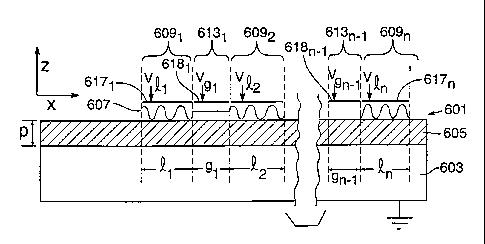
FIG. 6 is a schematic view of an exemplary coder in which voltages
can be applied independently to one or more corrugation segments or
spacer segments. A voltage V~1 applied to a selected corrugation segment
tunes a center frequency of the selected corrugation segment using a
refractive-index variation produced by the electro-optic effect. A voltage Vg1
CA 02360937 2001-07-25
WO 00/43828 PCT/US00/02154
3
applied to a selected spacer segment produces a programmable phase shift
proportional to Vgt .
FIG. 7 is a perspective view of a coder similar to that of FIG. 6 and
having a ground plane and control electrodes situated on a surface of a
substrate in which a waveguide core is defined. Electrodes corresponding to
individual corrugation segments are situated on the waveguide core and a
common electrode or ground plane is displaced from the waveguide core.
FIG. 8 is a sectional view of another exemplary coder that produces
phase shifts by electro-optic tuning of corrugation segments with applied
voltages sufficient to produce selected phase shifts but small enough so that
central wavelengths of the corrugation segments remain within a design
bandwidth.
FIG. 9 illustrates operation of a time-wavelength multiple access
("TWMA") coder in which a TWMA coded output of duration ~e is produced
by spectrally filtering an input pulse of pulse duration ~;~ to produce a
series
of output pulses of pulse duration ~~ and having respective central
wavelengths ~,;, amplitudes a;, and phases ~;, wherein ~; and ~,; are
programmably selected by applying voltages to corresponding segments.
FIG. 10 is a graph representing a TWMA code, illustrating an
occupancy of time and wavelength slots specified by the TWMA code.
FIG. 11 is a schematic view of a programmable TWMA coder formed
on an electro-optic substrate and to which independent voltages can be
applied to one or more corrugation or spacer segments. A voltage VQ.
T
applied to a selected corrugation segment tunes a respective grating
spacing and a center wavelength ~,; of the selected corrugation segment. A
CA 02360937 2001-07-25
WO 00/43828 PCT/US00/02154
4
voltage YgJ applied to a selected spacer segment tunes a respective phase
shift.
FIG. 12 is a schematic view of a TWMA coder in which a delay is
specified for a wavelength 7~; by electro-optically tuning a corrugation
segment.
FIG. 13 is a schematic view of a coder that has corrugation segments
defined by a corresponding corrugation of a mold.
FIG. 14 is a sectional view of a coder in which a surface of a
waveguide is physically or chemically processed to form one or more
corrugation segments in a waveguide formed in an electro-optic substrate.
FIGS. 15A-15B are perspective and sectional views, respectively, of a
coder having corrugation segments that comprise refractive index
modulations in a core of a waveguide. Dark and light segments correspond
to waveguide regions having high and low indices of refraction, respectively.
FIG. 16 illustrates a holographic exposure method for producing
index-of refraction modulations in a waveguide core.
FIG. 17 illustrates a method for producing a coder using a phase
mask to produce refractive-index modulations in a waveguide core.
FIG. 18 is a perspective view of a waveguide having a liquid crystal
cladding layer.
FIG. 19 is a sectional view of a corrugated waveguide having several
corrugation segments that have corresponding corrugation periods, wherein
CA 02360937 2001-07-25
WO 00/43828 PCT/US00/02154
the corrugated waveguide is electro-optically, thermally, mechanically, or
otherwise tunable.
Detailed Description
5 As used herein, a "programmable" device is a device having
properties that are electrically, thermally, mechanically, or otherwise
tunable
after manufacture of the device is complete. Programmable devices include
waveguides, waveguide gratings, corrugation segments and spacer
segments of waveguides, and coders using such waveguides and
waveguide segments. "Coder" and "code generator" are used herein to refer
to devices that either encode an input to produce an encoded output or that
decode an input to produce a decoded output. Coders can encode and
decode phase codes, amplitudes codes, or other codes. "Corrugation
segments" are waveguide segments that include a variation in one or more
optical properties. Such variations can be periodic with a single period or
multiply periodic (a sum of several variations of different periods). More
complex variations are also possible such as chirped variations in which the
period of the variation changes continuously. Waveguide regions that
contain no periodic variations but that are programmable to adjust a phase
or other parameter of an optical pulse are referred to as "spacer segments."
In some embodiments, spacer segments are provided to permit phase
modulation. As used herein, "tunable" refers to a device that imparts a
phase, amplitude, or other modulation to incident electromagnetic radiation,
wherein the modulation can be programmatically adjusted after device
manufacture.
Example embodiments are described that include "linear" electro-
optic materials that exhibit the Pockets effect. As used herein, an "electro-
optic" material is any material in which an applied voltage, electric field,
or
magnetic field produces a change in an optical property of the material.
Waveguides that include programmable composite gratings defined in
a core or a cladding or other layer of a waveguide are provided. According
CA 02360937 2001-07-25
WO 00/43828 PCT/US00/02154
6
to a specific embodiment, a programmable coder includes an optical
waveguide having an electrically controllable index of refraction in one or
more spatially distinct waveguide segments, each segment having a periodic
refractive-index modulation.
Other example embodiments include one or more channel
waveguides fabricated in an electro-optic material. The channel waveguides
comprise alternating grating segments and phase-shift segments (spacer
segments). The channel waveguides include one or more electrodes so that
voltages applied to the grating segments are independently controllable to
adjust a Bragg wavelength of each grating segment. The channel
waveguides also include phase-shift segments that are independently
controllable, so that optical delays or phase shifts between grating segments
are independently controllable. An input pulse with bandwidth sufficient to
span the operational bandwidth of such a channel waveguide (i.e., an input
pulse having a bandwidth that spans the center frequencies of all grating
segments of the channel waveguide) produces a diffracted output that
comprises a set of spectrally and temporally selected subpulses with
programmed phase shifts and frequencies. The bandwidth and center
frequency of a particular subpulse depend upon the grating segment that
produced that subpulse. Output timing (and hence phase) of the subpulse is
determined by a spatial position of the grating that produced the subpulse
and of the index of refraction of the grating segments and phase-shifting
segments through which that subpulse is transmitted before exiting the
channel waveguide.
Additional examples, methods, and features are described below with
reference to the accompanying drawings.
With reference to FIG. 1, a waveguide 101 comprises a waveguide
core 105 in a lithium niobate substrate 103 or other electro-optic material or
other tunable optical material. The core 105 of the waveguide 101 provides
mode confinement along a y-axis and a z-axis so that radiation propagates
along the x-axis in the waveguide 101. The core 105 has a width q
(measured along the y-axis) and a depth p (measured along the z-axis). The
CA 02360937 2001-07-25
WO 00/43828 PCT/US00/02154
7
substrate 103 has a refractive index nso for light polarized in an ordinary
direction and nse for light polarized in an extraordinary direction. For the
lithium niobate waveguide of FIG. 1, the ordinary polarization direction is
parallel to the y-axis and the extraordinary polarization direction is
parallel to
the z-axis. The core 105 has refractive indices more-ofor ordinary
polarization
and noo,o-a for extraordinary polarization. The orientation of the waveguide
101 with respect to the crystalline axes of lithium niobate is selected to
take
advantage of lithium niobate's large electro-optic coefficient r33, but other
orientations are possible. Typically, an orientation of an electro-optic
substrate is selected to take advantage of any large electro-optic
coefficients, but can be selected for other reasons as well, such as to obtain
an electrical impedance match or to reduce acousto-optic effects.
The values of the refractive indices nso and nSe are determined by the
substrate (lithium niobate). The values of the refractive indices more-o and
score-a are determined by the substrate and the processing method used to
define the core 105. For example, in lithium niobate, the core 105 can be
fabricated by either titanium in-diffusion or proton in-diffusion to produce a
refractive-index change in the core 105. The core dimensions p, q are
selected in conjunction with the various refractive indices in order to
provide
desired waveguide properties. Typically, the dimensions and refractive
indices are selected to provide a single-mode waveguide in which only a
single waveguide mode is guided and other modes (higher-order modes) are
attenuated. In addition, the dimensions p, q can be selected for ease in
coupling radiation into and out of the channel waveguide 101. For example,
alignment tolerances for coupling radiation into a waveguide having large
values of the dimensions p, q are relatively large.
With reference to FIGS. 2A-2B, a waveguide 201 formed in a lithium
niobate substrate 203 includes a cladding layer 207 of thickness 8 and
refractive index naiad. The thickness B of the cladding layer 207 can be
CA 02360937 2001-07-25
WO 00/43828 PCT/US00/02154
8
modulated to produce an effective refractive index of modulation (i.e., an
index grating) in the waveguide 201.
With reference to FIG. 3, a waveguide 301 comprises a lithium
niobate substrate 303, a core 305, and a cladding layer 307 in which a
corrugation segment 309 is defined. The corrugation segment 309 has a
corrugation 311 characterized by a period A, a modulation depth a, and a
phase a. The phase a represents a relative phase of the corrugation 311
and is shown as a displacement of a corrugation maximum 321 from a
corrugation-segment boundary 323. The phase a is conveniently measured
in degrees or fractions of a wavelength.
The corrugation segment 309 can be produced by several methods.
For example, a corrugated stamp or die can be pressed against the cladding
layer 307 to surficially impress the corrugation segment into the surface of
the cladding layer. A single corrugated stamp can be used to produce
corrugation segments on several waveguides or the corrugated stamp can
remain in contact with the cladding layer 307 and become part of the
waveguide 301.
With reference to FIG. 4, a waveguide 401 includes a core 405 of
refractive index more formed in a substrate 403 and a cladding layer 407 of
refractive index n~~aa. Corrugation segments 409; of lengths .2;, for
i = 1, . . . , n, separated by spacer segments 413; of lengths g; for
i = 1, . . ., n-1 are defined in the cladding layer 407. Each of the
corrugation
segments 409; has a central diffraction wavelength ~,; that depends on a
corresponding corrugation period A; according to a Bragg condition:
A; _ ~.; ~2ne~e~r;,,e
wherein neffe~c~~e is an effective index of refraction for propagation of
electromagnetic radiation in a guided mode in the waveguide 401. The
effective index neffe~t~"e generally depends on the refractive indices more,
n~~aa
as well the waveguide dimensions, shape, and order of the propagating
mode. In addition to the corrugation period A;, each corrugation segment
409; has a corresponding phase a; and a modulation depth a;. The lengths
CA 02360937 2001-07-25
WO 00/43828 PCT/US00/02154
~; , g; of the corrugation segments 409; and spacer segments 413;,
respectively, are selected to achieve desired spectral filtering functions.
The
spectral filtering functions also depend on the cladding refractive index
n~;ad,
the modulation depths 6;, and the core refractive index more.
For the lithium niobate waveguides of FIGS. 1, 2A-2B, and 3-4,
waveguide properties can be electrically controlled using the electro-optic
effect. Tuning of both the corrugation and spacer segments can be
achieved by applying respective voltages to these segments. Alternatively,
the waveguides can be controlled by controlling the respective temperatures
of the corrugation and spacer segments. The spacer segments provide
programmable phase tuning, while the corrugation segments provide
programmable center wavelengths as well as phase tuning. Tuning of a
corrugation segment typically tunes both the center wavelength and the
phase of the corrugation segment.
FIG. 5 illustrates operation of a coder 503. An input pulse 501 of
duration ~;" is incident to the coder 503. The coder 503 spectrally filters
the
input pulse 501 and produces a corresponding coded output 505 having a
duration ~e. Such a coded output can be used as a temporal identification
code in an optical code division multiple access ("CDMA") system or for
other applications. The coded output 505 comprises a series of output
pulses 507; each having a respective pulse duration ~~, respective amplitude
a;, and respective phase ~;, wherein i = 1, . . ., n. While the output pulses
507; of FIG. 5 are temporally separated from each other, the duration ~~ also
can be selected so that the output pulses 507; completely or partially overlap
each other. In addition, the pulse duration ~~ need not be the same for each
of the pulses 507;. Typically, each of the pulses 507; includes programmably
selected spectral components of the input pulse 501.
With reference to FIG. 6, a waveguide coder 601 comprises a core
605, a substrate 603, and a cladding layer 607. Corrugation segments 609;
and spacer segments 613; are defined in the cladding layer 607 and are
CA 02360937 2001-07-25
WO 00/43828 PCT/US00/02154
controlled by respective independent voltages V~J , Vgl applied to respective
electrodes 617;, 618;. The voltage V~J applied to an ith corrugation segment
609; controls a respective grating period A; via the linear electro-optic
effect,
thereby changing a respective center diffraction wavelength ~,; of the
5 corrugation segment 609;. The voltage VgJ applied to an ith spacer segment
613; produces a respective variable phase shift proportional to Vgt . The
electrodes 617;, 618; are shown positioned above the cladding layer 607, but
are generally conductive layers deposited directly on the cladding layer 607.
As an example, a coder configured to produce an output of 8 pulses,
10 each having a 30-ps duration (z~ = 30 ps) in a lithium niobate substrate
(ne =
2.2) has 8 identical corrugation segments 609; of length ~ = cz~ /2n~o,.e = 2
mm, wherein c is the speed of light. For operation at a wavelength of 1550
nm, the corrugation period is A = ~.~2n~ore ~ or 352 nm. (The subscript i can
be dropped because the corrugation segments are identical.)
The voltages V~J , Vg~ are determined based on a change in refractive
index ~neo produced in an electro-optic material by application of a voltage V
to electrodes having a spacing d:
0n __ n3.2Vr
eo
wherein n is a refractive index with no applied voltage and r is an efficiency
factor pertaining to the efficiency with which the applied voltage produces a
refractive-index change, measured relative to the refractive-index change
that otherwise would be produced by using large, parallel plate electrodes.
In a corrugation segment, the refractive-index change Oneo changes the
respective center wavelength as well as the respective phase. In spacer
segments, the refractive-index change Oneo produces a respective phase
modulation.
While high voltages are generally required to produce substantial
phase changes in bulk electro-optic devices, lithium niobate waveguides of
CA 02360937 2001-07-25
WO 00/43828 PCT/US00/02154
11
length 1 cm have been built that have halfwave voltages of about 8 volts. (A
"halfwave voltage" is a voltage required to produce a 180-degree phase
shift.) A 2-mm long waveguide segment used in a double-pass geometry
has a halfwave voltage of about 20 volts. Lengths of spacer segments can
be chosen for small temporal gaps in a coded sequence or to reduce the
magnitude of the modulation voltages needed to permit high-speed
modulation. Longer segments permit lower modulation voltages.
With reference to FIG. 7, a waveguide 701 comprises a substrate 703
and a core 705. Control electrodes 707-710 are situated on a surface 717 of
the substrate 703 on a waveguide axis 713. A common electrode 719 (for
example, a ground plane) is also situated on the surface 717 but offset from
the axis 713. Selecting appropriate voltages to be applied to the control
electrodes 707-710 permits programmable selection of a respective center
wavelength or a respective phase for each of the corresponding corrugation
segments or spacer segments, respectively. (For clarity in showing the
electrodes 707-710, FIG. 7 does not show any corrugation segments or
spacer segments.)
With reference to FIG. 8, a waveguide coder 801 comprises a
substrate 803, a core 805, and a cladding layer 806. Corrugation segments
807; (807, . . ., 807N) are provided at a surface 811 of the core 805 and
have corresponding electrodes 809; (809, . . ., 809N). For clarity, the
electrodes 809, . . ., 809N are shown in FIG. 8 positioned above respective
corrugation segments 807, . . ., 807N but are generally deposited directly on
the cladding layer 806. The segment phases, amplitudes, and periods for
each corrugation segment 807; are not shown in FIG. 8. Phase shifting of
the output pulses in the coded output produced by the coder 801 is achieved
by electro-optic tuning of the corrugation segments 807; by an amount
sufficient to generate a desired phase shift but not so large as to tune a
central wavelength of any segment outside of a design bandwidth.
FIG. 9 illustrates operation of a time-wavelength multiple access
("TWMA") coder 901. An input pulse 903 of duration ~;~ is incident to the
coder 901 that spectrally filters the input pulse 903 and produces a TWMA-
CA 02360937 2004-08-16
WO 00143828 PCT/US00102154
12
coded output 905 of total duration ~e. As shown in FIG. 9, the input pulse
903 enters an input surface 921 of the coder 901 and the TWMA-coded
output 905 exits the surface 921 as well. The TWMA-coded output 905 can
be used as, for example, a temporal identification code in an optical CDMA
system. The TWMA-coded output 905 comprises a series of output pulses
911; (911 ~, . . ., 911 N), each pulse having a duration ~~ and a respective
central wavelength ~,; (~,~, . . ., 7~N), respective amplitude a; (a~, . . .,
aN), and
respective phase ~; (~~, . : ., ~N). The respective phases ~; and wavelengths
~,; are determined by control voltages applied to the coder 901 from a
controller 951.
A TWMA code, as described in U.S. Patent No. 6,292,282 issued 18 September,
2001 to Mossberg, et. al., specifies a coded output as a series of pulses,
each pulse
having an assigned wavelength (or wavelengths) and occurring in one or
more assigned time slots. A graphical depiction of a representative TWMA
code is given in FIG. 10. TWMA codes can specify pulses in all available
time slots, at all available wavelengths, or can have one or more empty time
slots. In addition, TWMA codes can have more than one wavelength
component in one or more time slots, and can use the same wavelength in
more than one time slot. TWMA codes can be coherent or incoherent
codes, wherein a coherent code maintains a specified phase relationship
between wavelength components in different time slots.
With reference to FIG. 11, a TWMA code generator 1101 includes a
series of corrugation segments 1103; (1103, . . ., 1103N) and spacer
segments 1105; (1105, . , ., 1105~.~) formed on a waveguide core 1107.
Corrugations of respective corrugation segments 1103; (1103, . . ., 1'103,~~
have respective spatial periods A; (A~ , . . ., AN). Independent voltages can
be applied to the corrugation and spacer segments. A voltage Vp applied to
a particular corrugation segment 1103; tunes a respective grating period A; of
the corrugation segment 1103; by the electro-optic effect. This, in turn,
tunes
a respective central diffraction wavelength ~,; of the corrugation segment
CA 02360937 2001-07-25
WO 00/43828 PCT/US00/02154
13
1103;. A respective voltage Vgl applied to a particular spacer segment 1105;
produces a respective variable phase (time) shift that is proportional to Vg~
.
The spatial corrugation periods A~ , . . ., AN in different corrugation
segments
1103, . . ., 1103N can be equal or can be different to span a wider
wavelength range than obtainable using electro-optic tuning only.
The coder 1101 receives an input pulse 1151 and produces a TWMA
coded output 1161 that comprises a series of output pulses 1163;, wherein a
first output pulse 1163 is produced by diffraction from the corrugation
segment 1103, a second output pulse 11632 is produced by diffraction from
the corrugation segment 11032, and so on. Therefore, a Bragg wavelength
~; of the corrugation segment 1103; is tuned to diffract the desired
wavelength for the ith output pulse 1163;. In coherent TWMA, the spacer
segment 1105 between the first and second corrugation segments 1103,
11032 is used to adjust the phase between the first output pulse 1163 and
the second output pulse 11632. The remaining spacer segments 1105; are
used in a similar manner. As shown in FIG. 11, the coder 1101 produces a
coded output, but the coder 1101 also can serve as a decoder, receiving a
coded input and producing a decoded output.
With reference to FIG. 12, a waveguide coder 1201 comprises a
substrate 1203 and a cladding layer 1205, and includes a plurality of
corrugation segments 1209; each having a corresponding length l;.
Programmable delays for a selected wavelength ~,; are obtained by electro-
optic tuning of the center wavelengths of those corrugation segments 1209;
that produce the selected respective delays for the respective wavelengths
Additional embodiments are illustrated in FIGS. 13, 14, and 15A-15B.
With reference to FIG. 13, a waveguide coder 1301 comprises a core 1305
and a substrate 1303. A corrugated substrate 1307 is applied to a surface
1309 of the substrate 1303, and no additional molding steps are necessary.
FIG. 14 illustrates a waveguide coder 1401 that includes a core 1405 that is
physically or chemically processed to form corrugations 1411 directly on a
CA 02360937 2001-07-25
WO 00/43828 PCT/US00/02154
14
surface 1407 of the core 1405. Such corrugations can be formed by, for
example, reactive ion etching. Referring to FIGS. 15A-15B, a waveguide
coder 1501 comprises a core 1505 of dimensions p, q with corrugation
segments 1507 having refractive-index modulations in the core 1505. The
waveguide coder 1501 also includes spacer segments 1509 and electrodes
1513, 1515 for the corrugation segments and the spacer segments,
respectively. Parameters Ve. , ~; and Vgl , g; have the same meanings used
previously, and refer to a voltage applied to and a length of an ith
corrugation segment and a voltage applied to and a length of an ith spacer
segment, respectively.
With reference to FIG. 16, a holographic exposure method for
generating refractive-index modulations in a core of a waveguide includes
applying a photoresist layer 1603 to a substrate 1601. The photoresist layer
1603 is exposed with two write beams 1607, 1609 that interfere to produce a
spatial periodicity corresponding to a desired spatial period of a refractive-
index variation in a core of a waveguide. A mask 1611 prevents the write
beams 1607, 1609 from illuminating areas of the substrate 1601 in which
gratings of other periods (or no gratings at all) are to be formed. The
photoresist layer 1603 is developed, and the spatial modulation in the
photoresist layer 1603 is transferred to the core 1603 by a chemical
processing technique. Gratings with spatial periods as short as 292 nm can
be produced in lithium niobate waveguides using a proton-exchange process
to define the gratings. As discussed above, the proton-exchange process
(as known in the art) can also be used to define the core 1603.
FIG. 17 illustrates an exposure technique using a phase mask 1703 to
generate segments 1707 having refractive-index modulations in a core 1705
of a channel waveguide 1701. A photoresist layer 1711 on a surface 1713
of the core 1705 is exposed to a spatial modulation caused by an
interference, produced by the phase mask 1703, of a write beam 1717. This
spatial modulation is transferred from the exposed photoresist layer 1711 to
the core 1705 through chemical processing techniques as described above.
CA 02360937 2001-07-25
WO 00/43828 PCT/US00/02154
The methods illustrated in FIGS. 16-17 can also be used to write
refractive-index gratings in a core of a waveguide through the photo-
refractive effect. In this case, the gratings are written by exposing the
substrate to radition having a wavelength to which the substrate is photo-
5 refractively sensitive. For lithium niobate, green light can be used.
The code generators, coders, and waveguides described above are
described with reference to channel waveguides in a lithium niobate
substrate. Alternatively, other electro-optic substrate materials can be used,
such as lithium tantalate, potassium niobate, gallium arsenide, ADP, KDP,
10 RTA, and others. In addition to electro-optic substrates, the code
generators
can be fabricated in any of various other substrates capable of supporting a
waveguide. In addition to channel waveguides, fiber waveguides or other
waveguide geometries can be used.
Gratings or other corrugations can also be produced in a core or a
15 cladding of a waveguide formed in an isotropic (or non-electro-optic)
substrate such as glass. Such gratings are temperature- and strain-tunable.
For example, a coder that comprises fiber Bragg gratings can be tuned by
local heating or by imposition of local strains to modify the Bragg
wavelengths of the grating segments and the phase shifts between the
grating segments.
Gratings also can be formed using a liquid crystal overlay. With
reference to FIG. 18, a channel waveguide 1801 includes a core 1805
formed in a substrate 1803. A liquid crystal layer 1807 covers at least a
portion of the core 1805 and/or the substrate 1803. Local indices of
refraction of the liquid crystal layer are electrically controlled by applying
respective voltages V; to respective electrodes 1811; to produce a localized
reorientation in the liquid crystal layer. Corrugation segments, grating
segments, or spacer segments can be defined by the electrodes 1811;. For
example, to produce a corrugation region, an electrode to which a voltage V
is applied can be divided into a periodic array of electrodes such as the
electrode 1811~_~. Alternatively, corrugation segments and spacer segments
CA 02360937 2001-07-25
WO 00/43828 PCT/US00/02154
16
can be defined in the core 1805, and the electrodes 1811; can be used to
tune preexisting corrugations.
Additional embodiments include two or more matched or unmatched
programmable coders as described above and incorporated into arms of a
Mach-Zehnder, Michelson, or other interferometer. Independent tuning of
different segments in the coders in each of the arms permits complex
modulations to be achieved, including amplitude modulations that are not
achievable with a single coder. In further embodiments, coders comprise
corrugation segments having several corrugation periods, i.e., that are
"multiply periodic" gratings (gratings having multiple periods). Such
segments can diffract multiple wavelengths, thereby enabling the coding and
decoding of complex codes. In addition, the respective lengths of the
corrugation segments and of the spacer segments can be different from one
another.
In yet another variation, the corrugation segments have multiple
corrugation periods, and a difference in center wavelengths diffracted by
different corrugation segments is larger than a bandwidth of the incident
radiation. With reference to FIG. 19, by tuning a waveguide 1901 through
mechanical, electro-optic, thermal, or other means, a different code can be
coded. For example, a coder can comprise n controllable corrugation
segments, each corrugation segment having a refractive-index modulation
characterized by two periods, a first period and a second period, that are not
necessarily equal for all corrugation segments. If a first control voltage is
applied, then incident radiation is diffracted from the first period of each
corrugation segment, producing a first coded output. If a second control
voltage is applied, then incident radiation is diffracted from the second
period
of each corrugation segment, producing a second coded output. In general,
this approach can be used to generate N codes, each code corresponding to
a particular control voltage. The structure of a kth grating segment can be
written as a superposition of periodic corrugations:
N
Gk - ~ nik eXp~l~ik
i=1
CA 02360937 2001-07-25
WO 00/43828 PCT/US00/02154
17
where ~;k is the phase shift of the ith corrugation on the kth corrugation
segment, and A;k is the wavelength of the ith corrugation on the kth
corrugation segment.
In an alternate embodiment, different codes are encoded in spatially
distinct segments of a waveguide. In this case, only those segments that are
resonant with incident radiation diffract the incident radiation to produce a
coded output. Thermal, mechanical, or electro-optic tuning can be used to
select among codes multiplexed in this manner.
While the principles of the invention have been described with
reference to example embodiments, it will be appreciated by those skilled in
the art that these example can be modified without departing from the spirit
and scope of these principles. The example embodiments are not to be
taken as limiting the scope of the invention, and we claim all that is
encompassed by the appended claims.