Note: Descriptions are shown in the official language in which they were submitted.
CA 02360970 2001-11-01
la
A WIRELESS MICROPHONE HAVING A SPLIT-BANb AUDIO
FREQUENCY COMPANDING SYSTEM THAT PROVIDES
IMPROVED NOISE REDUCTION AND SOUND QUALITY
Field of the Invention
This invention generally relates to wireless microphone systems and, more
particularly, to a wireless microphone systenn having a split-band audio
frequency
companding system that provides improved noise reduction and sound quality
with reduced cost.
Backiground of the Invention
Companding circuits that include a cotnpressor circuit and an expander
circuit may be used to increase the useable dynamic range of a signal that
passes
through a modulated space. In audio applications, this is done by first
compressing
the dynamic range of the information signal prior to modulation, and then
expanding the dynamic range of the information signal after demodulation.
Referring to Figs lA and 1B, general, schematic representations of a typical
compression circuit 10 and a typical expansion circuit 12, respectively, are
shown.
In the circuit shown in Fig. lA, a rectifier and filter element 14 is used to
detect the amplitude of an input signal at terminal 16. The amplitude
information
is utilized to control the resistance of a variable resistance element 18 that
is
provided in the feedback loop of an operational amplifier 20. This circuitry
is
arranged so that relatively higher amplitude information generally reduces the
resistance of the variable resistance element 18, while relatively lower
amplitude
information generally increases the resistance of the variable resistance
element
20. This has the effect, for example, of reducing the gain of amplifier 20 for
higher level signals at terniinal 16, and of increasing the gain of amplifier
20 for
lower level signals at terminal 16. Signal processing is continuously done
across
the frequency spectrum for signals of low amplitudes to signals of high
amplitudes.
CA 02360970 2001-11-01
-'2.
Fig. 1 B is a general, schematic diagram of a typical expander circuit 12 that
is used to expand the dynamio range of the signal at termizxa122. Circuit 12
includes generally the same circuit components that form the compression
circuit
shown in Fig. 1A, such components including a variable resistance element 24,
a
rectifier and filter element 26, an operational amplifier 28, and a feedback
resistor
30. However, the circuit components shown in Fig. 1 B are reanranged as shown
so
that the gain of the operational amplifier 28 increases as the amplitude of
the signal
at terminal 22 increases, and so that the gain of the operational amplifier 28
decreases as the amplitude of the signal at terminal 22 decreases.
The problems associated with such compandor circuitry are largely due to
the time conBtant of the integrating filter of the rectifier that forms a
portion of the
rectifier and filter components 14 and 26 (Figs. 1A and 1B). If the time
constant is
made relatively large, then amplitude modulation of the higher frequency
components of the noise by lower frequency components of the signal can be
heard
by a user. This is commonly referred to as "breathing," which is undesirable,
especially in high-end audio applications.
Signals with a quick rise time often are distorted by typical compandor
circuits because, for example, the compressor circuit portion of the compandor
circuit may not be able to react fast enough to keep the signal within the
linear
range of the modulated space. If the time constant is short, "breathing" goes
away,
but lower frequency signals become distorted due to rectifier ripple. Both of
the
above-referenced problems are particularly evident in wide band audio
implementations such as, for example, wireless microphone applications.
Distortion problems can be reduced by establishing separate attack and
release time constants for the rectifiers that are used in the compression and
expansion circuits. However, there is still a serious compromise in
performance
that must be made for wide band signals present in high-end audio
applications.
Various specific compander circuits are known. See, for example, U.S.
Patent No. 4,353,035 that discloses a circuit for compression or expansion of
an
electrical signal. This patent states that a two-band compander pre-emphasis
is
CA 02360970 2008-07-30
-3-
carried out during compression and de-emphasis during expansion in the lower
frequency range. This patent states that noise suppression is improved by the
pre-
emphasis and de-emphasis operations.
In another application, U.S. Patent No. 4,449,106 discloses a noise
reducing apparatus that includes a circuit that processes signals in a
plurality of
frequency bands. This patent states that the mid and high frequencies are
intensified when the signal level is low. This patent also states that the
signal level
versus noise level ratio in the mid and high frequency ranges is increased
with
respect to the noise introduced in the transmission path.
In yet another application, U.S. Patent No. 5,832,097 discloses a multi-
channel synchronous companding system for hearing aids. This patent states
that
an input signal is directed through a 2:1 compressor, and then is directed
through a
band splitting filter to divide the signal into a desired number of frequency
bands.
This patent further states that the divided signals are then passed through
expander/compressors to provide selected expansion/compression of each
frequency band as a function of the user's hearing impairment.
The above-described circuits are suitable for their intended purposes.
However, such circuits may not be suitable for a number of applications such
as,
for example, high end wireless microphone applications. In such applications,
a
premium is placed on the quality of the audio reproduction. Also, a premium is
placed on the ability to manufacture such microphones with reduced cost that
allows the manufacturer's profit margin to be maximized. Furthermore, battery
life is a concern in the transmitter portion of typical wireless microphones
because
the presence of a greater number of active elements increases current drain
and
correspondingly decreases battery life.
CA 02360970 2001-11-01
-4-
Suwnmarv of the Invention
It is desirable to provide a wireless microphone having a multi-band audio
companding system. One aspect of the present invention is that the companding
system includes a compression circuit in which one amplification element is
utilized in connection with a number of frequency bands, each frequency band
having a rectifier and filter element associated therewith. A further aspect
of the
present invention is that high-pass filter elements are utilized in the higher
frequency bands of the compression and expander circuits to reduce the
transfer of
low-frequency signals to the rectifier elements that process the high-
frequency
signals, thereby reducing undesirable modulations of a variable resistance
element
associated therewith.
Providing a wireless microphone with such a companding system has a
number of distinct advantages. First, the time constants of the integrating
filter of
the rectifier utilized in the compression and expansion circuits are
individually set
with respect to each frequency band that is processed, thereby allowing
improved
audio reproduction. Second, breathing problems are reduced. Third, problems
associated with rectifier ripple are minimized. Fourth, the material costs
associated with raanufacturin.g such a wireless microphone are significantly
reduced because a smaller number of circuit components are utilized.
Other features and advantages of the invention will become apparent from
the description that follows.
Descriotion of the Drawings
Figs. 1A is a general, schematic representation of a prior art compression
circuit;
Fig. 1B is a general, schematic representation of a prior art expansion
circuit;
CA 02360970 2001-11-01
~5-
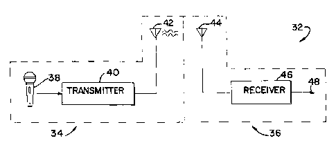
Fig. 2 is a general, schematic representation of a wireless microphone
system that incorporates a split-band audio frequency companding system that
provides improved noise reduction and sound quality;
Fig. 3A is a general, schematic representation of the transmitter portion 34
of the wireless microphone system 32 shown in Fig. 2;
Fig. 3B is a general, schematic representation of the receiver portion 36 of
the wireless microphone system 32 shown in Fig. 2;
Fig. 4A is a general, schematic representation of the compressor circuit 52
shown in Fig. 3A;
Fig. 4B is a general, schematic representation of the expander circuit 66
shown in Fig. 3B;
Fig. 5 is a detailed schematic diagram of a specific application of the
compressor circuit 66 shown in Fig. 4A;
Fig. 6 is a detailed schematic diagram of a specific application of the
expander circuit shown in Fig. 4B; and
Fig. 7 is a graph that illustrates the audio performance of the companding
circuitry illustrated in Figs. 5 and 6 that is utilized in the wireless
microphone
system shown in Fig. 2.
Detailed Description of the Invention
While the present invention is susceptible of embodiment in various forms,
there is shown in the drawings a number of presently prefen-ed embodiments
that
are discussed in greater detail hereafter. It should be understood that the
present
disclosure is to be considered as an exemplification of the present invention,
and is
not intended to limit the invention to the specific embodiments illustrated.
Fig. 2 is a general, schematic diagram of a wireless microphone system 32
that incorporates a split-band audio frequency companding system that provides
improved noise reduction and sound quality. System 32 includes a transmitter
portion 34 and a receiver portion 36. Transmitter portion 34 includes a
microphone 38, a transmitter circuit 40, and an antenna 42 that may be located
at a
CA 02360970 2008-07-30
-6-
first location when the system 32 is in use. In an exemplary application of
the
present invention, microphone 36 may be a directional microphone such as, for
example, the digital and analog microphone disclosed in U.S. Patent No.
6,084,973.
The receiver portion 36 of the wireless microphone system 32 includes an
antenna 44 and a receiver circuit 46. The receiver portion 36 produces an
audio
level output signal at terminal 48.
Fig. 3A is a general, schematic representation of the transmitter portion 34
of the wireless microphone system 32 shown in F'sg. 2. Transmitter portion 34
includes an audio frequency amplifier 50 that amplifies the signal provided to
it
from microphone 38. A unique compressor circuit 52 compresses the signal
provided to it at terminal 52a from amplifier 50, and provides a compressed
signal
at tenninal 52b as discussed in greater detail hereafter. Radio frequency
oscillator
54, modulator 56, and radio frequency amplifier 58 are utilized to provide a
modulated and amplified signal to antenna 42 that is broadcast therefrom. It
should be understood that any suitable means of modulation such as, for
example,
amplitude or frequency modulation techniques may be utilized in connection
with
the present invention.
Fig. 3B is a general, schematic representation of the receiver portion 36 of
the wireless microphone system 32 shown in Fig. 2. Receiver portion 36
includes
a radio frequency amplifier 60 that provides an amplified signal to the tuning
and
amplification circuit 62 that is operatively coupled to a local oscillator 64.
An
expander 66 is eloctrically coupled to the tuning and demodulation circuit 62
via
terminal 62a to allow an audio output signal to be provided at terminal 48 via
terminal 62b and audio frequency amplifier 68 as discussed in greater detail
hereafter.
Fig. 4A is a general, schematic representation of the compressor circuit 52
shown in Fig. 2A, while Fig. 4B is a general, schematic representation of the
expander circuit 66 shown, in Fig. 2B. In the embodiment of the present
invention
CA 02360970 2001-11-01
-7-
illustrated in Figs. 4A and 4B, two frequency bands are utilized to allow low
and
high frequency signals to be companded separately in two distinct frequency
bands. However, it should be understood that any number of frequency bands can
be utilized in accordance with the principles of the present invention
disclosed in
this application.
Referring to Fig. 4A, a low-frequency rectifier 70 and a high-frequency
rectifier 72 are utilized for compression purposes. Each rectifier 70 and 72
is
provided with separate attack and release time constants as discussed in
greater
detail hereafter. Two variable resistance elements 74 and 76 are provided in
the
feedback loop of operational amplifier 78. A low-pass filter 80 and a high-
pass
filter 82 are electrically coupled to the inputs of the variable resistance
elements 74
and 76, respectively. A high-pass filter 84 is electrically coupled to the
high-
frequency rectifier 72 as shown in Fig. 4A.
Compression circuit 52 includes an attack capacitor 86 and a release
capacitor 88 that are operatively electrically coupled to the low-frequency
rectifier
70. Capacitors 86 and 88 are optimized for frequencies below the crossover
point.
An attack capacitor 90 and a release capacitor 92 are operatively electrically
coupled to the high frequency rectifier 72 as shown in Fig. 4A. Capacitors 90
and
92 are optimized for frequencies above the cross-over point.
In operation, the low-pass filter 80 causes the low-frequency adjustable
resistance element 74 to control the gain of operational amplifier 78 at
frequencies
below the crossover point. Similarly, the high-pass filter 82 causes the high-
frequency adjustable resistance element 76 to control the gain of the
operational
amplifier 78 at frequencies above the crossover point. High-pass filter 84
reduces
the transfer of low-frequency components into the high-frequency rectifier 72
that
would create hartnonics that would modulate the high frequency adjustable
resistance element 76. Modulation of component 76 in this manner is especially
undesirable in high-end audio applications.
CA 02360970 2001-11-01
-8-
Referring to Fig. 4B, the expander circuit 66 includes a low-frequency
rectifier 94 and a high-frequency rectifier 96. Rectifiers 94 and 96 include
attack
capacitors 98 and 100, as well as release capacitors 102 and 104,
respectively, that
provide separate attack and release time constants for each rectifier. The
attack
and release capacitors 98 and 102 on low-frequency rectifier 94 are optimized
for
frequencies below the crossover point, and are equal to the timing capacitors
on
low-frequency rectifier 70 (Fig. 4A). Likewise, the attack and release times
for
high-frequency rectifier 96 are optinzized for frequencies above the crossover
point, and are equal to the timing capacitors on high-frequency rectifier 72.
Expander circuit 66 also includes two high-pass filters 106 and 108, a low-
pass filter 110, a low-frequency variable resistance element 112, a high-
frequency
variable resistance element 114, and two operational amplifiers 116 and 118.
Appropriate resistors 120 and 122 are provided in a feedbaclc loop of the
operational amplifiers 116 and 118 as shown.
In operation, high-pass filter 106 causes the high-$equency variable
resistance element 114 to control the gain of operational amplifier 116 above
the
crossover point. Similarly, the gain of operational amplifier 116 is
controlled for
low frequencies by the low-frequency variable resistance element 112. However,
the output of operational amplifier 118 is filtered by low-pass filter 110.
Placing
low-pass filter 110 after the operational amplifier 118 is advantageous
because, for
example, a reduction in noise and distortion over placing it before the
operational
amplifier 118 is obtained.
High-pass filter 108 reduces the transfer of low frequency signal
components from entering high-frequency rectifier 96. This provides a number
of
distinct advantages such as, for example, a reduction in the production of
harmonics that would modulate the high-frequency variable resistance element
114
in an undesirable manner. The high and low expanded components are summed
via resistors 124 and 126 to create a single output signal at terminal 62b.
CA 02360970 2001-11-01
-9-
The crossover frequency between the two frequency bands utilized in the
compressor circuit 52 and the expander circuit 66 is determined by the time
constants of the following circuit components: high-pass filter 82, high-pass
filter
84, high-pass filter 106, high-pass filter 108, low-pass filter 80, and low-
pass filter
110. In the illustrated embodiment of the invention, the time constants of
these
filter elements are all generally equal to each other.
Figs. 5 and 6 are detailed schematic diagrams of a specific implementation
of the compression circuit 52 and the expander circuit 66 shown in Fig. 2. In
the
embodiment of the invention illustrated in Figs. 5 and 6, four commercially
available programmable analog compander circuits 128, 130, 132, and 134 are
utilized. A circuit that is preferred for this application is available from
Phillips
Semiconductors as programmable analog compander circuit model no. SA572.
Use of such circuit components provides a number of distinct advantages such
as,
for example, allowing for scparate attack and release timing capacitors.
Referring to Fig. 5, R3 and C4 correspond to the low-pass filter 80 shown
in Fig. 4A. C12 and a 6.8K resistor that is internal to the circuit 130 form
the
high-pass filter element 82 shown in Fig. 4a. The high pass-filter element 84
(Fig.
4A) is formed from C 18 and R12. C6 and C3 correspond to the attack and
release
capacitors 86 and 88 (Fig. 4A), while C14 and C16 correspond to attack and
release capacitors 90 and 92 (Fig. 4A). The low-frequency rectifier 70 and the
low-frequency variable resistanee element 74 (Fig. 4A) are irxternal to
compandor
circuit 128, while high-frequency rectifier 72 and the high-frequency variable
resistance element 76 (k'xg. 4A) are internal to the compander circuit 130.
Referring to Fig. 6, R12 and C23 form the low-pass fiater 110 (Fig. 4B).
C8 and a 6.8K resistor that is internal to the compandor circuit 132 form the
high-
pass filter 106 (Fig. 4B). The high pass filter 108 shown in Fig. 4B is fonned
from
C 15 and R7 shown in Fig. S. C 13 and C 10 correspond to attack capacitor 100
and
release capacitor 104 (Fig. 4B),.while C24 and C21 correspond to attack
capacitor
98 and release capacitor 102. Low-frequency rectifier 94 and low-frequency
variable resistance element 112 are intenul to compander circuit 134. High-
CA 02360970 2001-11-01
-10-
$equency rectifier 96 and high-frequency variable resistance element 114 are
internal to compander circuit 132. Amplifier 136 is a buffer amplifier that is
used
to drive the expander circuit, while amplifier 138 a sumnung amplifier.
Fig. 7 shows the excellent frequency and atnplitude linearity of the
connpanding circuitry shown in Figs. 4A and 4B across the full audio band.
Lineacity in this manner is quite desirable for high-end audio applications
such as
wireless microphone applications.
The illustrated embodiments of the present invention concern wireless
microphone applications. However, it should be understood that the unique
split-
band companding circuitry disclosed herein may be utilixed in other
applications
such as, for example, wireless musical instsuments such as electric guitars,
electric
bases and the like.
From the foregoing it will be observed that numerous modifications and
variations can be effectuated without departing from the true spirit and scope
of
the novel concepts of the present invention. It is to be understood that no
liniitation with respect to the specific embodiments illustrated is intended
or
should be infen-ed. The disclosure is intended to cover by the appended claims
all
such modifications as fall within the scope of the claims when the claims are
properly interpreted.