Note: Descriptions are shown in the official language in which they were submitted.
CA 02360972 2001-11-O1
SEMICONDUCTOR LASER MODULE
AND
RAMAN AMPLIFIER USING THE MODULE
BACKGROUND OF THE INVENTTnN
1. Field of the Invention
The present invention relates to a semiconductor laser
module which is capable of being employed as a pumping light
source of an optical amplifier, and an optical amplifier which
is capable of being employed in optical communication.
2. Description of the Related Art
In existing optical fiber communication systems, there
have been frequently employed rare earth doped fiber amplifiers.
In particular, there have been more frequently employed an
erbium doped optical fiber amplifier to which erbium (Er) has
been doped (hereinafter referred to as "EDFA"). The practical
gain wavelength band of the EDFA is in a range between about
1530 nm and about 1610 nm. Also, the EDFA has a wavelength
dependency, and in the case where the EDFA is used in a wavelength
division multiplexing signal light, the gain changes in
accordance with the wavelength of the signal light.
In the midst of on-going dense wavelength division
multiplexing (DWDM), a Raman amplifier has been increasingly
expected as an amplifying system having a broader broadband than
that of the EDFA. Upon making an intensive light (pumping
light) putted into an optical fiber, the Raman amplification
has a peak of the gain at a longer wavelength side (a frequency
lower by about 13 THz assuming that the pumping light of 1400
nm band is applied) from the pumping optical wavelength by about
100 nm due to induced Raman scattering. The Raman
amplification is an optical signal amplifying method using such
a phenomenon that when the signal light having the wavelength
band by which the above gain is obtained enters the optical fiber
thus excited, the signal light is amplified.
The EDFA has the practical gain wavelength band ranging
from about 1530 nm to about 1610 nm whereas the Raman
1
CA 02360972 2001-11-O1
amplification hardly has a limit of the wavelength band
(because it is presumed that a range between 1300 and 1650 nm
is used in fact, the wavelength band of the pumping light is
in a range between 1200 and 1550 nm) . If the wavelength of the
pumping light putted into the optical fiber changes, the gain
appears at a longer wavelength side from the wavelength of the
pumping light by a predetermined wavelength, and therefore an
amplified gain can be obtained at an arbitrary wavelength. For
that reason, according to the wavelength division multiplexing
(WDM), the number of channels for the signal lights can be
further increased.
The above gain has a gain distribution with a wavelength
distribution, for example, a distribution having a width of
about 20 nm because glass molecules of which the optical fiber
is made have a variety of vibration poses. In order to make
the wavelength dependency of the gain flat over the broader
wavelength band, the pumping lights of various wavelengths are
multiplexed to appropriately adjust the wavelengths, the
outputs and so on of the respective pumping lasers . In the Raman
amplification, the existing optical fibers for communication
can be employed as amplifying medium, and the Raman gain in the
case of employing the existing optical fibers is small to the
degree of about 3 dB when the pumping light of 100 mW is inputted.
For that reason, there is required that an intensive pumping
light is obtained by multiplexing. In general, the pumping
light from about 500 nw to about 1 W in total is normally obtained
by multiplexing.
As the pumping light source used in the Raman amplifier,
there is used a semiconductor laser module that stabilizes the
wavelengths due to f fiber bragg grating ( FBG ) and outputs a high
power light.
One of the semiconductor laser modules with the FBG is
shown in Fig. 6. A laser beam emitted from a semiconductor laser
device A is converted into a collimated beam through a first
lens B, and the collimated beam is condensed onto an input end
face of an optical fiber D through a second lens C, to thereby
2
CA 02360972 2001-11-O1
optically couple the semiconductor laser device A with the
optical fiber D. The optical fiber D is formed with a fiber
grating E that reflects only a light having a predetermined
wavelength. In the semiconductor laser module shown in Fig.
6, a Peltier device P for temperature control is disposed within
a package F, a base K is disposed on the Peltier device P, and
a photodiode (PD) for monitoring, a thermister S and the
semiconductor laser device A are mounted on the base K. As shown
in Fig. 7, the FBG thus structured has, for example, a
reflectivity spectrum whose peak reflectivity is about 4% and
whose full width half maximum (FWHM) is 2 nm, and feeds back
only a part of the laser beam coupled with the optical fiber
D to the semiconductor laser device A. Because a loss of an
external resonator made up of the semiconductor laser device
A and the FBG becomes smaller at only the center wavelength of
the FBG, even in the case where a driving current or an ambient
temperature of the semiconductor laser device A changes, the
oscillation wavelength of the semiconductor laser device A is
fixed at the above center wave.
However, there arises the following problems in
employment of the semiconductor laser module with the FBG as
shown in Fig. 6 as the pumping light source for the Raman
ampl if ier .
Because the Raman gain is small in the Raman amplification
as described above, a high output of the pumping light source
is required not only as a total optical output in a state where
a plurality of semiconductor laser modules are multiplexed but
also as an optical output of a semiconductor laser module single
substance.
Moreover, a demand for providing a higher optical output
in the semiconductor laser module has been increased year by
year from the viewpoints of long-distance transmission and a
reduction in the number of optical amplifiers in the optical
communication.
In order to meet that demand, there is a method in which
the peak reflectivity of the FBG at the front end face side of
3
CA 02360972 2001-11-O1
the semiconductor laser device is lessened in the structure
shown in Fig. 6. However, if the peak reflectivity of the FBG
is lessened, the lead-in effect of the oscillation wavelength
to an FBG predetermined wavelength in the semiconductor laser
device is weakened, thereby making it difficult to stabilize
the wavelength. As a result, a driving current range of the
semiconductor laser device which is available in a state where
the wavelength is stabilized is restricted, and the optical
output that is available substantially at the maximum is not
improved.
As described above, the conventional semiconductor laser
module suffers from the difficulty of providing the higher
optical output.
SUMMARY OF THE INVENTION
The present invention has been made to solve the above
problems with the conventional device, and therefore an object
of the present invention is to provide a semiconductor laser
module that is capable of realizing a higher optical output
which is suitable for the pumping light source of a Raman
amplifier and excellent in a wavelength stability.
In order to achieve the above object, according to a first
aspect of the present invention, there is provided a
semiconductor laser module comprising: a semiconductor laser
device having a cavity length of 800 ,um or longer; an optical
fiber that receives a laser beam outputted from said
semiconductor laser device and transmits the laser beam;
wherein a fiber bragg grating (FBG) disposed at the rear of said
semiconductor laser device through a lensed fiber and a cavity
is defined between said FBG and said semiconductor device. The
semiconductor laser module has a collimating lens and a
condenser.
According to a second aspect of the present invention,
in the semiconductor laser module according to the first aspect
of the invention, an antireflection coating having 1~ or more
reflectivity is formed on a front end face of the semiconductor
4
CA 02360972 2001-11-O1
laser device, and an antireflection coating having less than
1~ reflectivity is formed on a rear end face of the semiconductor
laser device.
According to a third aspect of the present invention, in
the semiconductor laser module according to the first or second
aspect of the invention, an antireflection coating having 5~
or less reflectivity is formed on a front end face of the
semiconductor laser device.
According to a fourth aspect of the present invention,
in the semiconductor laser module according to any one of the
first to third aspects of the invention, the collimating lens
and the condenser are disposed between the font end face of the
semiconductor laser device and the optical fiber, and an
isolator is disposed between the collimating lens and the
condenser.
According to a fifth aspect of the present invention, in
the semiconductor laser module according to any one of the first
to fourth aspects of the invention, the FBG is formed in the
lensed fiber, a rear end face of the lensed fiber is inclined
or vertical, and a photodiode ( PD ) for monitoring is disposed
at the rear of the rear end face of the lensed fiber.
According to a sixth aspect of the present invention,
in the semiconductor laser module according to any one of the
first to fifth aspects of the invention, two or more FBGs are
formed in the lensed fiber, and the reflection center
wavelengths of the two or more FBGs are identical with or
different from each other.
According to a seventh aspect of the present invention,
in the semiconductor laser module according to any one of the
first to sixth aspects of the invention, the full width at half
maximum of the FBG is any one of 1 nm or more and 5 nm or less,
and the reflectivity of the FBG is 50~ or more.
According to an eighth aspect of the present invention,
in the semiconductor laser module according to any one of the
first to seventh aspects of the invention, the semiconductor
laser device, the lensed fiber with the FBG and the isolator
5
CA 02360972 2001-11-O1
are mounted on a base whose temperature is controlled by a
Peltier device.
A Raman amplifier according to the present invention uses
the semiconductor laser module as defined in any one of the first
to eighth aspects of the invention.
According to the present inventors' study, the following
characteristics are requiredfor thesemiconductor laser module
used as a pumping light source of the Raman amplifier. It is
preferable that the semiconductor laser module according to the
present invention further satisfies the following required
characteristics.
a) A noise of the pumping light is small:
The noise of the pumping light is -130 dB/Hz or less when
an RIN (relative intensity noise) is in a range from 0 to 2 GHz
(in a range from 0 to 22 GHz as occasion demands).
b) The degree of polarization (DOP) is small:
It is necessary that a coherent length is short, that is,
a multimode is provided and depolarizing is liable to occur,
or that no polarization occurs due to polarization multiplexing.
The provision of the multimode may be satisfied by making at
least three longitudinal modes, preferably four to five
longitudinal modes enter within an oscillation spectrum (a
width of a wavelength coming down from the peak of the spectrum
by 3 dB.
c) The optical output is high:
The optical output of the semiconductor laser module is
required to be 50 mW or more, preferably 100 mW or more, more
preferably 300 mW or more, and most preferably 400 mW or more.
d) The wavelength stability is excellent:
Because a fluctuation of the oscillation wavelength leads
to a fluctuation of the gain wavelength band, a technique for
stabilizing a lazing wavelength due to a fiber grating, a DFB
laser (distributed-feedback laser), a DBR laser (distributed
brag reflector laser) or the like is required. It is necessary
that the fluctuation width is, for example, within ~ 1 nm under
all of driving conditions (an ambient temperature: 0 to 75 0
6
CA 02360972 2001-11-O1
C, a driving current: 0 to 1 A).
e) The oscillation spectrums of the respective
pumping laser modules are narrow:
If the oscillation spectrums of the respective pumping
laser modules are too broad, the coupling loss of the wavelength
multiplexing coupler becomes large, and the number of
longitudinal modes contained within the spectrum width becomes
large, as a result of which the longitudinal mode moves during
oscillation, and the noise and gain may fluctuate. In order
to prevent that drawback, it is necessary to set the oscillation
spectrum to 2 nm or less, or 3 mm or less. If the oscillation
spectrum is too narrow, a kink appears in the current to optical
output characteristic, and a failure may occur in the control
during laser driving. If at least three longitudinal modes,
preferably four or five longitudinal modes enter in the
oscillation spectrum as described in the above item b), it is
presumed that the coherency is reduced, thereby being liable
to reduce the DOP.
f) The power consumption is low:
Because polarization multiplexing, wavelength
multiplexing and so on are applied, a large number of pumping
lasers are employed. As a result, the entire power consumption
becomes large. It is preferable that the power consumption of
the pumping laser module single substance is low.
g) No SBS (stimulated brillouin scattering) occurs:
When a higher optical output is concentrated in a narrow
wavelength band due to the fiber grating or the like, the SBS
occurs to deteriorate the pumping efficiency. From this
viewpoint, the multimode (a plurality of longitudinal modes
exist within the oscillation spectrum) is proper.
h) High PIB (power in band):
When lights of plural wavelengths are coupled together,
a demand is made to output the laser beam having a relatively
narrow linear width of PIB ~ 90~ within the wavelength width
2 nm from the viewpoint of the higher optical output.
i) It is preferable to install the isolator:
7
CA 02360972 2001-11-O1
In order to prevent the laser operation from being
unstabilized due to a reflection light, it is preferable to
dispose an isolator within the semiconductor laser module.
BRTEF DESCRIPTION OF THE DRAWINGS
These and other objects and advantages of this invention
will become more fully apparent from the following detailed
description taken with the accompanying drawings in which:
Fig. 1 is a side view showing the entire outline of a
semiconductor laser module in accordance with the present
invention;
Fig. 2 is a detailed explanatory diagram showing an
example of the main portion of the semiconductor laser module
shown in Fig. 1;
Fig. 3 is a detailed explanatory diagram showing another
example of the main portion of the semiconductor laser module
shown in Fig. 1;
Fig. 4 is an explanatory diagram showing a Raman amplifier
in accordance with an embodiment of the present invention;
Fig. 5 is an explanatory diagram showing a Raman amplifier
in accordance with another embodiment of the present invention;
Fig. 6 is an explanatory diagram showing a conventional
semiconductor laser module; and
Fig. 7 is an explanatory diagram showing the operation
of the semiconductor laser module shown in Fig. 6.
17FTATT,ED DESCRIPTION
Now, a description will be given in more detail of
preferred embodiments of the present invention with reference
to the accompanying drawings.
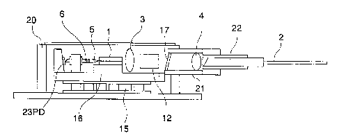
A semiconductor laser module in accordance with a first
embodiment of the present invention is shown in Fig. 1. The
semiconductor laser module includes a PD 23, a lensed fiber 5
with an FBG, a semiconductor laser device 1, a first lens
(collimating lens ) 3 which converts a laser beam emitted from
the semiconductor laser device 1 into a collimated beam, and
8
CA 02360972 2001-11-O1
an isolator 12 within a package 20. Among those components,
the PD 23, the lensed fiber 5 with an FBG, and the semiconductor
laser device 1 are mounted on a base 16 whose temperature is
controlled by a Peltier device 15. A fitting jig 21 is fitted
into the package 20, a second lens (condenser) 4 that condenses
the laser beam emitted from the isolator 12 is received within
the fitting jig 21, and a ferrule 22 into which an optical fiber
2 is inserted and connected is fixedly inserted into the fitting
j ig 21. With the above structure, the PD 2 3 , the lensed f fiber
with an FBG, the semiconductor laser device 1, the collimating
lens 3, the isolator 12 and the optical fiber 2 are disposed
in a line on an optical axis.
In order to realize the higher optical output as a pumping
light source in the Raman amplifier, the semiconductor laser
device 1 requires a cavity length of 800 ,um or more.
A first embodiment of the components in Fig. 1 is shown
in Fig. 2. The lensed fiber 5 shown in Fig. 2 has a front end
that has been processed into a lens shape such as a spherical
leading shape or a wedge shape so that the fiber per se is
converted into a micro lens, and a rear end of the fiber is cut
obliquely upward so that reflection is reduced. For example,
in the case where the front end of the lensed fiber 5 is
wedge-shaped, the front end is provided with a wedge angle
corresponding to the astigmatim of the semiconductor laser
device 1 so as to enhance the coupling efficiency. An
antireflection coating (AR coating) is formed on each of the
front end face and the rear end face of the lensed fiber 5, and
the reflectivity of those antireflection coatings is desirably
set to 0.5% or less (substancially, about 0.1%): An FBG 6 is
formed at the front end side of the lensed fiber 5. The FBG
6 is 1 to 5 nm in the full width at half maximum and 50 to 90%
in the peak reflectivity. The oscillation wavelength of the
semiconductor laser device 1 is locked by the FBG 6. In Fig.
1, a wave selection filter 17 is disposed between the isolator
12 and the condenser 4.
Fig. 2 shows the main portion of the semiconductor laser
9
CA 02360972 2001-11-O1
module shown in Fig. 1.
The rear end face 10 of the semiconductor laser device
1 shown in Fig. 2 is coated with an antireflection coating (AR)
11 whereas the front end face 8 thereof is coated with an
antireflection coating (AR coating) 9. A dielectric
multilayer coating is suitable for the AR coating. The
dielectric multilayer coating may be made of the combination
of Ta205 and Si02, Ti02 and Si02, A1203 and Si02, and so on.
The reflectivity of the AR coating 9 on the front end face
8 is set to, for example, 1 to 5%, and the reflectivity of the
AR film 11 on the rear end face 10 is set to, for example, less
than 1%, preferably 0.5% or less.
In Fig. 2, an external resonator (external cavity) 7 is
made up of the FBG 6 and the AR coating 11 of the rear end face
10 of the semiconductor laser device 1, and the FBG 6 and the
AR coating 9 on the front end face of the semiconductor laser
device 1. The cavity length of the external cavity 7 is
adjustable by changing a position of the semiconductor laser
device 1 or the FBG 6, and an optical path length between the
rear end face 10 of the semiconductor laser device 1 and the
FBG 6 is preferably set to 75 mm or less from the viewpoint of
a reduction in noise.
The existing components can be employed for the
collimating lens 3, the isolator 12 and the condenser 4 shown
in Fig. 1, respectively. For example, an aspherical lens, a
ball lens, a distributed refractive lens or a plano-convex lens
may be employed for the collimating lens 3. Those focal
distances f are suitably set to 0 . 4 to 2 mm ( usually f = about
0.7 to 0.8 mm). Antireflection coatings (AR coatings) are
formed on both of the front and rear end faces of the collimating
lens 3, respectively, and their reflectivity is preferably set
to 0.5% or less. Likewise, an aspherical lens, a ball lens,
a distributed refractive lens or a plano-convex lens may be
employed for the condenser 4. Those focal distances f are
suitably set to 1 to 5 mm (usually f - about 3 mm).
Antireflection coatings (AR coatings ) are formed on both of the
CA 02360972 2001-11-O1
front and rear end faces of the condenser 4, respectively, and
their reflectivity is preferably set to 0.5~ or less. The
collimating lens 3 and the condenser 4 are related to the MFD
NA of the semiconductor laser device 1 and the MFD~NA of the
fiber. The isolator 12 may be of the polarization dependency
type.
The optical fiber 2 may be formed of a polarization
maintaining fiber (PMF) other than a single mode optical fiber
( SMF ) . In this s ituation, the polarization is saved by making
the polarization maintaining axis (a slow axis or a fast axis)
of the PMF coincide with the polarization direction of the laser
beam. Also, in order to conduct depolarizing, the polarization
maintaining axis of the PMF may be made to coincide with a
direction that rotates by 45 degrees with respect to the
polarization direction. The input end face (within a ferrule)
of the SMF may be so shaped as to be cut vertically or obliquely
by 5 to 20 degrees (in fact, 6 to 8 degrees), or shaped into
a leading spherical fiber. It is preferable that an
antireflection coating 0.5 or less (in fact, 0.1~) in the
reflectivity is disposed on the input end face, but the input
end face may be kept to be obliquely cut without provision of
the antireflection coating.
A lens may be disposed or not disposed in front of the
PD 23 shown in Fig. 1. In order to prevent the laser beam
inputted onto the photodiode 23 from being reflected and then
returned to the interior of the external cavity, it is
preferable that the light input face of the PD 23 is inclined
with respect to the optical axis.
In the semiconductor laser module of this embodiment, the
provision of the FBG 6 makes it possible to stabilize the
wavelength and improve the PIB. Also, the reflection spectrum
of the FBG 6 is controlled, thereby being capable of realizing
a reduction in the SBS and easing a reduction in the DOP.
The FBG 6 is disposed at the rear of the semiconductor
laser device 1, and since the peak reflectivity can be set to
a high reflectivity of, for example, 50~ or more, the lead-
11
CA 02360972 2001-11-O1
in of the oscillation wavelength to the predetermined
wavelength in the FBG 6 is sufficient.
Also, when the FBG 6 is thus disposed, and the reflectivity
of the AR coating 9 on the front end face 8 of the semiconductor
laser device 1 is set to a value lower than, for example, 5%
or less, a high optical output can be obtained in the
semiconductor laser module.
Likewise, with the provision of the FBG 6 at the rear of
the semiconductor laser device 1, the isolator 12 can be
disposed between the front end face 8 of the semiconductor laser
device 1 and the light input end face of the optical fiber 2.
The isolator 12 may be of the polarization dependent type
because the laser beam which has not yet been inputted to the
optical fiber 2 is linear polarization whose polarization plane
is determined in a constant direction. The isolator of the
polarization dependent type can be inexpensive and low in the
optical loss as compared with the isolator of the polarization
independent type. The opticalloss of the typicalpolarization
independent type isolator is about 1dB whereas the optical loss
of the polarization dependent type is about 0.3 dB.
The application of the lensed fiber makes it possible to
shorten a distance between the semiconductor laser device 1 and
the FBG 6, thereby improving a noise characteristic in a
predetermined frequency range.
(Second Embodiment)
A second embodiment of the components shown in Fig. 1 is
shown in Fig. 3. In Fig. 3, a semiconductor laser device 1,
a first lens (collimating lens) 3 that converts a laser beam
emitted from the semiconductor laser device 1 into a collimated
beam, an isolator 12, a second lens (condenser) 4, a ferrule
22 and an optical fiber 2 are identical in structure with those
in Fig. 2, and the lensed fiber 5 in Fig. 3 is different from
that in Fig. 2.
Two FBGs 6 are formed on the lensed fiber 5 shown in Fig.
3. The provision of those two FBGs 6 can more stabilize the
wavelength of a light outputted from the semiconductor laser
12
CA 02360972 2001-11-O1
module. Those two FBGs 6 may be identical in the reflection
center wavelength with each other, or slightly different in the
reflection center wavelength from each other. Fig. 4 shows the
structure of an embodiment of a Kaman amplifier 100 using the
semiconductor laser module described in the above-mentioned
respective embodiments as a pumping light source module. The
Kaman amplifier shown in Fig. 4 is directed to an optical
amplifier of a co-pumping method including a plurality of laser
units 101 that output lights different in wavelength, a WDM
coupler 102 that wavelength-multiplexes the lights outputted
from the laser units 101, and an optical fiber 103 that transmits
the wavelength-multiplexed light.
Each of the laser units 101 includes the semiconductor
laser module 105 described in any one of the above-mentioned
respective embodiments, an optical fiber 106 that transmits the
laser beam outputted from the semiconductor laser module 105,
a depolarizes 107 formed of a PMF inserted into the optical fiber
106, and a control section 108.
The semiconductor laser module 105 outputs the laser
beams different in wavelength from each other on the basis of
the operation control of the semiconductor laser device by the
control section 108, for example, the control of an inrush
current or a Peltier module temperature. An isolator of the
polarization dependent type is disposed within the
semiconductor laser module 105 as in Figs. 1 to 3, to thereby
prevent the reflection light to the semiconductor laser device.
The depolarizes 107 is directed to, for example, a
polarization maintaining f fiber disposed in at least a part of
the optical fiber 106, and its coherent axis is inclined by 45
degrees with respect to the polarization plane of the laser beam
outputted from the semiconductor laser module 105. With this
arrangement, the DOP of the laser beam outputted from the
semiconductor laser module 105 is reduced, thereby being
capable of making depolarization.
In the Kaman amplifier 100 thus structured, after the DOP
of the laser beam outputted from each of the semiconductor laser
13
CA 02360972 2001-11-O1
modules 105 has been reduced by the depolarizer 107, the laser
beams different in wavelength are combined together by the WDM
coupler 102 , and then inputted into the optical f fiber 110
through which a signal light is transmitted, through the optical
fiber 103 and the WDM coupler 109.
The signal light within the optical fiber 110 is
transmitted while being Raman-amplified by the inputted laser
beam (pumping light).
In the Raman amplifier 100 of the present invention, the
use of the semiconductor laser module 105 and the laser unit
101 according to the present invention makes it possible to
obtain the Raman gain excellent in the wavelength stabilization
and high in the optical level.
Fig. 5 shows the structure of another embodiment of the
Raman amplifier 100 using the above-mentioned semiconductor
laser module as the pumping light source module. In Fig. 5,
the Raman amplifier 111 is directed to an optical amplifier of
the co-pumping method including a plurality of laser units 101
that output lights different in wavelength, a WDM coupler 102
that wavelength-multiplexesthelightsoutputted from the laser
units 101, and an optical fiber 103 that transmits the
wavelength-multiplexed lights.
Each of the laser units 101 includes the two semiconductor
laser modules 105 described in any one of the above-mentioned
respective embodiments, optical fibers 106 that transmits the
laser beams outputted from the semiconductor laser modules 105,
respectively, a PBC (polarization beam combiner) 112 that
polarization-combines those laser beams, an optical fiber that
transmits the combined light, and a control section 108 that
forms a control means of the present invention.
The above-mentioned plurality of semiconductor laser
modules 105 output the laser beams different in wavelength from
each other on the basis of the operation control of the
semiconductor laser device by the control section 108, for
example, the control of an inrush current or a Peltier module
temperature. An isolator of the polarization dependent type
14
CA 02360972 2001-11-O1
is disposed within each of the semiconductor laser modules 105
as in Figs. 1 to 3, to thereby prevent the reflection light to
the semiconductor laser device.
After the polarizations of the laser beams outputted from
each of the semiconductor laser modules 105 of the Raman
amplifier 111, which are identical in the wavelength and
different in the polarization plane, have been combined by the
PBC 112 and the degree of polarization has been reduced, the
lights different in the wavelength are further combined by the
WDM coupler 102, and then inputted into the optical fiber 110
through which the signal light is transmitted, through the
optical fiber 103 and the WDM coupler 109.
The signal light within the optical fiber 110 is
transmitted while being Raman-amplified by the inputted laser
beam (pumping light).
In the Raman amplifier 111 of the present invention, the
use of the semiconductor laser modules 105 and the laser unit
101 according to the present invention makes it possible to
obtain the Raman gain excellent in the wavelength stabilization
and high in the optical level.
The present invention is not limited to the above-
mentioned embodiments, but can be variously modified within the
subject matter of the present invention.
Also, in the above-mentioned respective embodiments, the
description was given of the Raman amplifier of the co-pumping
method by which the present invention can be particularly
suitably employed. However, the present invention is not
limited to this, but can be applied to the Raman amplifier of
the rearward pumping method or the bi-directional pumping
method.
Effects of the invention
As was described above, the semiconductor laser module
according to the present invention can realize the higher
optical output which is suitable for the pumping light source
of the Raman amplifier and excellent in the wavelength
CA 02360972 2001-11-O1
stabilization.
Also, in the semiconductor laser module according to the
present invention, since the isolator is disposed between the
semiconductor laser device and the input end face of the optical
fiber, the reflection light is prevented, the laser oscillation
is stabilized, the loss is less than that of an in-line, and
higher output is enabled.
The foregoing description of the preferred embodiments
of the invention has been presented for purposes of illustration
and description. It is not intended to be exhaustive or to limit
the invention to the precise form disclosed, and modifications
and variations are possible in light of the above teachings or
may be acquired from practice of the invention. The embodiments
were chosen and described in order to explain the principles
of the invention and its practical application to enable one
skilled in the art to utilize the invention in various
embodiments and with various modifications as are suited to the
particular use contemplated. It is intended that the scope of
the invention be defined by the claims appended hereto, and
their equivalents.
16