Note: Descriptions are shown in the official language in which they were submitted.
CA 02360979 2001-07-19
1
SPECIFICATION
TITLE OF THE INVENTION
Method of and apparatus for spread spectrum reception
TECHNICAL FIELD
The present invention relates to a spread spectrum
reception apparatus. More particularly, this invention
relates to detection of RAKE-combination signal for
detecting a signal proper for the RAKE-combination.
BACKGROUND ART
When transmitting an information signal, a spread
spectrum reception apparatus which performs communication
using DS-CDMA (Direct Sequence CDMA) system operates as
follows. That is, it applies a first modulation such as
QPSK to the information signal and thereafter
spread-modulates the information signal with a spread code
such as PN sequence to transmit it. When receiving such
a spread spectrum signal, the spread spectrum reception
apparatus at a reception side as follows . That is, it
calculates a correlation value between a received spread
spectrum signal and a predetermined spread code to detect
a synchronization phase of spread code. Thereafter, it
produces an inverse-spread of the received spread spectrum
CA 02360979 2001-07-19
2
signal using the inverse-spread signal. Such inverse
spread signal is then information-modulated to obtain the
information signal.
During mobile communication, a portion of a
transmissionsignalisreflected, diffracted, andscattered
by topography or construction such as buildings to reach
a reception side via different routes and at different times .
For example, a reflected wave, which is the one that is
reflected by construction, reaches the reception side later
than a direct transmission wave, which is the one that
directly reaching from the transmission side to the reception
side. The reason behind this is that, the route of the
reflection wave is longer than that of the direct wave. Time
difference between when the direct wave reaches the reception
side and when the delay wave, that is the reflection wave
that has been delayed, will be substantially about a few
10 microseconds. The route of the signal traveling from
a transmission side to a reception side is referred as "path"
Transmission environment wherein a transmission signal
travels via a plurality of paths is referred as "multipath" .
Under multipath environment, a reception side is destined
to receive a multiplex wave . In a multiplex wave, signals
of a plurality of paths of which delay times are different
are overlapped because a plurality of same spread spectrum
signals respectively reach at different times. In mobile
CA 02360979 2001-07-19
3
communication, there is a motion on the transmission side
or the reception side. Therefore, during mobile
communication, fading, which is an alternation in
amplification of multiplex wave, occurs. Thefading occurs
because a way in which the phrases are combined always changes
due to the motion of the transmission side or the reception
side.
A RAKE-receiver is the one which RAKE-combines
(maximum-ratio-combines) a signal output from a plurality
of RAKE-fingers for separating five predetermined path
signals by inverse-spreading a received multiplex wave with
a combiner to perform a weight application corresponding
to a reception signal level. Signal-electric-power-ratio
against thermal noise and interference of a received
multipath signal is improved by performing RAKE reception,
so that diversity reception is realized. However, it is
necessary to select a plurality of path signals proper for
RAKE-combinationin ordertoinverse-spreadeach pathsignal
from a multiplex wave to perform RAKE-combination.
The selection of path signals proper for
RAKE-combination is performed with a delay profile
indicating a correlation value calculated with a reception
spread spectrum signal and a predetermined reference spread
code and a delay time therein by each sample point . It is
considered that an information signal is included in a signal
CA 02360979 2001-07-19
4
whose correlation electric power value is greater among
sampling points of the delay profile. Therefore, it will
be better to select a signal of the sampling points at which
the correlation electric power value is greater as a signal
of the path proper for RAKE-combination. For example, in
a case of a spread spectrum receiver provided with three
sets of RAKE-fingers for inverse-spreading, there will be
three RAKE-combinable paths. In this case, as shown in Fig.
18, a method for selecting a signal of path of detecting
three sampling points in order having highest correlation
value may be adopted.
If there is no time-correlation in thermal noise and
interference among the sampling points shown in Fig. 18,
then a sampling point is detected in order by a point whose
correlation value is greater and thereafter inverse-spread
signals are RAKE-combined respectively corresponding to a
delay time of the detected sampling points. Thus, signal
electric powerScstandardized withinterferenceand thermal
noise after RAKE-combination becomes maximum and may be
represented by following equation. Si is directed to a
correlation electric power value in the i-th order detection
path timing.
3
Sc=~ Si
i=1
However, there exists a time correlation in thermal
CA 02360979 2001-07-19
noise and interference among real sampling points.
Therefore, if signals of path detected in order from a greater
correlation value are merely combined, a signal electric
power Sc will be reduced. The amplitude of signal electric
5 power Sc is concretely represented by following equation.
Herein, s= (sl, s2, s3) T and si is directed to a correlation
value corresponding to timing i.
~STS~2
SC =
S~F~S
,~'t.~ ,x'1.2 ~ ~.3
R = ,rte 2 . '~ p 2 . 2 ,~ ,2 . 3
,~ 3 . '~ ~a 3 . 2 ,ra ~ . 3
pij is directed to time correlation coefficient of
noise and interference between timings i and j. Namely,
the narrower, a distance between sampling points to be
detected is, in other word, when arrival times are
extraordinarily close (when delaytimesaremutuallyclosed
in a delay profile ) , the greater, time correlation in thermal
noise and interference among these signals is . There exists
a method for detecting a sampling point in order from the
sampling point whose correlation value is greater by sampling
points whose delay time is sufficiently spaced with respect
to a detected sampling point as shown in Fig. 19 in order
to eliminate affection owing to time correlation of thermal
noise and interference among the sampling points and make
CA 02360979 2001-07-19
6
a signal electric power standardized with interference and
thermal noise.
Further, in Japanese Patent Laid-open Application No.
10-336072, a first path is detected by selecting a sampling
point whose correlation value is greatest in a delay profile
shown in Fig. 20 (refer to Fig. 20 (a) ) . Thereafter, sampling
points positioned within ~k numbers of sampling points (k
is a natural number) are eliminated from an object to be
selected with respect to sampling points having been already
detected and a second path is detected (refer to Fig. 20 (b) ) .
Next, a third path is detected by selecting a sampling point
whose correlation value is greatest from among sampling
points positioned except for within ~k numbers of sampling
points with respect to a sampling point of a second path
(refer to Fig. 20(c)). As above-explained, there exists
a method for selecting a path proper for RAKE-combination
by setting a distance between samples to be selected as a
distance corresponding to k or greater numbers of samples .
Furthermore,in JapanesePatentLaid-open Application
No. 10-308688, a delay profile is produced by performing
cyclic integration after electric power conversion in order
to perform average calculation by excluding affection of
fading alternation and a carrier frequency deviation at the
time of transmission and reception. Then, a theoretical
value of result of inverse-spread of a reference code and
CA 02360979 2001-07-19
7
an ideal reception signal and a portion where maximum
amplification portion of a correlation value is eliminated
by a pseudo correlation elimination portion is called from
a delay profile to have the delay profile impulse-shaped
whereby a path for RAKE-combination is detected.
Additionally, a theoretical value of result of
inverse-spread of a reference code and an ideal reception
signal with a matrix calculation of a reception signal
whereby a path for RAKE-combination is detected.
As above-explained, the reception side is destined
to receive a multiplex wave wherein signals whose delay times
are different have been overlapped under a multipath
environment, because transmitted spread spectrum signals
reach via a plurality of paths and at different times .
Therefore, in order to eliminate affection of mufti-fading,
numbers of signals corresponding to numbers of RAKE fingers
are selected by a delay profile produced by calculating a
correlation value between a predetermined reference spread
code and a reception multiplex signal to separate a path
signal by inverse-spreading a multiplex wave in accordance
with a delay time of a selected path signal to RAKE-combine
the separated path signals whereby a ratio of a signal
electric power to interference and thermal noise must be
improved. As a result, it is important how a path signal
proper for RAKE-combination should be selected in order to
CA 02360979 2001-07-19
8
optimize effect of improvement of the ratio relating to the
signal electric power with RAKE-combination.
For example, there exists little effect of improvement
of the ratio relating to the signal electric power with
RAKE-combination when time correlation of thermal noise and
interference between selected paths is too great . As above,
effect of improvement of the ratio relating to the signal
electric power with RAKE-combination is largely dependent
on correlation of thermal noise and interference of each
of path signals. Because numbers of RAKE-fingers forming
a RAKE-combination modulator are limited, a path signal whose
time correlation of thermal noise and interference are great
is not RAKE-combined, rather, a path signal whose time
correlation of thermal noise and interference are great is
RAKE-combined, so that the effect of RAKE-combination by
the latter becomes larger than an effect when path signals
are merely combined in order from a signal having greater
correlation value.
According to the technology disclosed in Japanese
PatentLaid-open Application No.lO-336072, sampling points
positioned within ~k numbers of sampling points are
eliminated from an object to be selected for a second path
with respect to sampling points detected as a first path,
so that there lies a problem that even if a sampling point
is one capable of improving characteristic with
CA 02360979 2001-07-19
9
RAKE-combination, the sampling point may not be detected
as a second path. There lies a possibility that
characteristic is deteriorated by RAKE-combination,
because a sampling point positioned except for within
k numbers of sampling points with respect to sampling points
detected as a first path, as a second path if a correlation
value is greater in spite of time correlation of thermal
noise and interference. Namely, there lies a possibility
that signal characteristic is further deteriorated if
inverse-spread signals are RAKE-combined corresponding to
a delay time of signal of each of detected paths, because
the paths are not detected, considering over time correlation
of thermal noise and interference.
According to the technology disclosed in Japanese
Patent Laid-open No. 10-308688, a delay profile is produced
by performing cyclic integration after electric power
conversion. However, affection owing to electrical power
conversion is not considered for this delay profile, so that
any optimum path may not be detected for RAKE-combination .
According to the conventional invention disclosed in
JapanesePatentLaid-open Application No.lO-308688,a delay
profile is made to be impulse-shaped and thereafter a path
to be RAKE-combined is detected. However, even a path such
as may improve characteristic by RAKE-combination is
destined to be cut off. Further, in a case of even a path
CA 02360979 2001-07-19
such as being deteriorated regarding as characteristic, if
an electric power is greater, then the path is destined to
be detected. Furthermore, a cyclic addition is performed
at a voltage level and a delay profile is corrected at a
5 voltage level . However, the correction may not be performed
because a ratio of a signal to interference of the delay
profile is too poor.
When a spread code whose period is longer than a symbol
period is used, or when length of already-known transmission
10 symbol sequence is longer, amount of calculation for
obtaining a theoretical value of inverse-spread result of
reference code and a reception signal becomes vast. This
will result in a larger circuit which consumes higher
electrical power, because, such a vast number of calculations
are performed by each time of detection of RAKE-combination
path timing. For example., if a cell radius exceeds over
about lOkm and a chip-rate exceeds over about 4 MHz, then
it must be considered that the delay spread is represented
by about 256 chips . Further, if the operation is performed
with 4-times-oversample, then a 1024 x 1024 matrix must be
inversed. This is not realistic, because calculation is
too vast to detect a signal of path proper for
RAKE-combination, following an environment of propagation
of mobile station moving with high-speed. Optionally,
there is no guarantee that such an inverse-matrix always
CA 02360979 2001-07-19
11
exists. As a result, there is possibility that the
inverse-matrix may not exist, so that a RAKE-combination
timing may not be detected.
According to the technology disclosed in Japanese
Patent Application No. 10-308688, a pseudo correlation
elimination portion for correcting a delay profile is
arranged independently of a synchronization detection
portion for detecting a path for RAKE-combination. As a
result, hardware become large scaled and it consumes higher
electric power.
The present invention is devised in order to overcome
the above-explained problems. It is an object of this
invention to select a path signal proper for RAKE-combination,
considering over a time correlation of thermal noise and
interference to RAKE-combine the selected path signals
whereby a spread spectrum reception apparatus for improving
a ratio of a signal electric power to interference and thermal
noise is provided.
DISCLOSURE OF THE INVENTION
The spread spectrum reception apparatus according to
the present invention is provided with a
RAKE-combination-unit and a RAKE-combination signal
detection unit. The RAKE-combination-unit includes a
plurality of inverse-spread units each of which
CA 02360979 2001-07-19
12
inverse-spreads a spread spectrum being signal
spread-modulated and transmitted, using an inverse-spread
code being delayed for a predetermined time whereby the
predetermined delay time signal is separated from the spread
spectrum signal; a combining unit which RAKE-combines the
signal inverse-spread by the inverse-spread units; and a
delay unit which delays the inverse-spread codes supplied
to the inverse-spreading units based on a delay control
signal input from outside. The RAKE-combination signal
detection unit includes a delay pro file generation unit which
generates a delay profile with a correlation electric power
value obtained by converting a correlation value of the
spread spectrum signal and a reference spread code into an
electric power and the delay time; a correction coefficient
storing unit which stores already calculated correction
coefficient based on time correlation between interference
and thermal noise by each deviation of the delay time; a
delay profile correction unit which measures a deviation
between a delay time of signal whose correlation electric
power value is maximum and a delay time of signal in the
delay profile and corrects a correlation electric power value
in the delay profile using a multiply value obtained by
multiplying a correction coefficient read from the
correction coefficient storing unit corresponding to the
measured deviation by a maximum electric power value in the
CA 02360979 2001-07-19
13
delay profile; and a signal detection unit which detects
a signal whose correlation electric power value becomes
maximum in the delay profile produced by the delay profile
producing unit to output a delay time of the detected signal
as a first delay control signal and a delay time of signal
whose correlation electric power value becomes maximum in
the corrected delay profile corrected by the delay profile
correction unit as a second delay control signal to the delay
unit.
Further, in the spread spectrum reception apparatus
according to the present invention, the delay profile
correction unit is provided with an average calculating unit
which calculates an average of the correlation electric power
value of the delay profile, and the delay profile correction
unit multiplies a value obtained by subtracting the average
calculated by the average calculating unit from a maximum
correlation electric power value in the delay profile by
a correction coefficient.
Further, in the spread spectrum reception apparatus
according to the present invention, the delay profile
producing unit is provided with a threshold value
discriminating unitwhich comparesthecorrelationelectric
power value with a predetermined threshold value and decides
whether the correlation electric power value is equal to
more than the threshold value, and the delay profile
CA 02360979 2001-07-19
14
producing unit produces a delay profile based on a
correlation electric power value that is greater than the
threshold value.
Further, in the spread spectrum reception apparatus
according to the present invention, the delay profile
producing unit is provided with a correlation electric power
value storing unit which stores the correlation electric
power value of a signal for which the threshold value
discriminating unitdecidesthatthecorrelation power value
is greater than the threshold value; and a delay time storing
unit which stores a delay time of the signal whose correlation
electric power value is greater than the threshold value .
The spread spectrum reception method according to the
present invention is a method of detecting a plurality of
signals whose correlation value is greater based on a delay
profile produced with a correlation value of a reception
spread spectrum signal and a reference spread code to use
an inverse-spread code delayed corresponding to a delay time
the detected signal to RAKE-combine signals separated from
the receptionspectrum spreadsignal. This methodincludes
the steps of producing a delay profile based on a correlation
electric power value obtained by converting the correlation
value to electric power; detecting a delay time of a signal
whose correlation electric power value is maximum of the
delay profile produced in the delay profile producing step;
CA 02360979 2001-07-19
measuring a deviation between the delay time detected in
the first RAKE-combination signal detection step and the
delay time of any other signal in the delay profile;
correctingthe delay profileusingacorrectioncoefficient
5 correspondingtothecalculated deviation, which correction
coefficient is obtained from already stored plurality of
correction coefficients calculated from time correlation
between interference and noise due to temperature, and the
correlation electric power value of a signal detected in
10 the first RAKE-combination signal detection step; and
detecting a delay time of signal whose correlation electric
power value becomes maximum based on the corrected delay
profile in the delay profile correction step.
Further, in the spread spectrum reception method
15 according to the present invention, at the delay profile
correction step an average of correlation electric power
values of the delay profile is calculated and the correlation
electric power value of the delay profile is corrected using
the calculated average.
Further, in the spread spectrum reception method
according to the present invention, at the delay profile
producing step, the correlation electric power value is
compared with a predetermined threshold value and a delay
profile is produced based on a signal whose correlation
electric power value is greater than the threshold value .
CA 02360979 2001-07-19
16
BRIEF DESCRIPTION OF THE DRAWINGS
Fig. 1 is a block diagram showing a construction of
a spread spectrum reception apparatus according to the
present invention. Fig. 2 is a block diagram showing a
construction of a RAKE-combination path timing detector
providedin aspreadspectrum receptionapparatusaccording
to a first embodiment of the present invention. Fig. 3 shows
the result of calculation of correlation value . Fig. 4 shows
the result of cyclic integration of electric voltage. Fig.
5 shows the produced delay profile (Doppler spread profile) .
Fig. 6 explains about a delay profile for using a first path
detection and the first path detection. Fig. 7 explains
about a delay profile for using a second path detection and
the second path detection. Fig. 8 is explains about a delay
profile for using a third path detection and the third path
detection. Fig. 9 is a block diagram showing a construction
of a RAKE-combination modulator. Fig. 10 is a flow chart
of a method of detecting RAKE-combination signal in a spread
spectrumreception method according tothepresentinvention.
Fig. 11 is a flow chart for explaining about a content of
a delay profile correction step. Fig. 12 is a block diagram
showing a construction of a RAKE-combination path timing
detector provided in a spread spectrum reception apparatus
according to a second embodiment of the present invention.
Fig. 13 shows a delay profile wherein a noise electric power
CA 02360979 2001-07-19
17
and an interference electric power are added. Fig. 14 is
a flow chart for explaining about a content of a delay profile
correction step. Fig. 15 is a block diagram showing a
construction of a RAKE-combination path timing detector
providedin aspreadspectrumreception apparatusaccording
to a third embodiment of the present invention. Fig. 16
is one showing an example of continuous measurement of delay
profile. Fig. 17 is a flow chart for explaining about a
step for producing a delay profile. Fig. 18 explains
conventional examples of path detection. Fig. 19 explains
conventional examples of path detection. Fig. 20 explains
conventional examples of path detection.
BEST MODE FOR CARRYING OUT THE INVENTION
The present invention will be explained in detail below
while referring to the accompanying drawings.
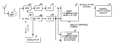
Fig. 1 is a block diagram showing a construction of
a spread spectrum reception apparatus according to the
present invention. Fig. 2 is a block diagram showing a
construction of a RAKE-combination path timing detector.
In Fig. 1, reference numeral 1 denotes an antenna, reference
numeral 2 denotes an RF amplifier, reference numerals 3A
and 3B denote mixers, reference numeral 4 denotes a local
oscillator, reference numeral 5 denotes a 90-degrees-phase
shifter, reference numerals 6A and 6B denote low pass filters,
CA 02360979 2001-07-19
18
reference numerals 7A and 7B denote A-D converters, reference
numeral8denotestheRAKE-combination pathtiming detector,
reference numeral 9 denotes a RAKE-combination modulator,
and reference numeral 10 denotes a digital processing
circuit.
The construction and the operation thereof will be
explained hereinafter. The local oscillator 4 supplies a
local oscillation having a frequency substantially equal
to a frequency of a desired signal to the mixers 3A and 3B.
The 90-degrees-phase shifter 5 is arranged between the mixer
3B and the local oscillator 4 . The 90-degrees-phase shifter
590-degrees-phase-shiftsalocaloscillationsignaloutput
from the local oscillator 4 to output the shifted local
oscillation signal to the mixer 3B. In addition to the local
oscillation signal, a multiplex signal received through the
antenna 1 and amplified by the RF amplifier 2 and divided
into two channels is input into the mixers 3A and 3B. The
mixers 3A and 3B, the local oscillator 4, and 90-degree-phase
shifters thus quadrature-detect areceivedspreadspectrum
signal to output I-channel and Q-channel base band signals .
I-channel base band signal is input from the mixer
3A to the low pass filter 6A. Q-channel base band signal
is input from the mixer 3B to the low pass filter 6B. The
low path filter 6A filters the I-channel base band signal,
and the low path filter 6B filters the Q-channel base band
CA 02360979 2001-07-19
19
signal to pick up a desired signal . These filtered I-channel
and Q-channel base band signals are respectively output to
A-D converters 7A and 7B, where the analog signal is converted
to digital signal.
The A-D converters 7A and 7B respectively sample the
analog I-channel and Q-channel base band signals to obtain
digital signals. The I-channel and Q-channel digital
signal are output to the RAKE-combination path timing
detector 8 and the RAKE-combination modulator 9.
The operation performed by the RAKE-combination path
timing detector 8 and the RAKE-combination modulator 9 will
be explained hereinafter. Under a multipath environment,
as already-explained, the transmitted spread spectrum
signals reach via a plurality of paths and at different times,
so that a reception side receives a multiplex wave wherein
signals whose delay times are different are overlapped.
Therefore, following procedureisrequiredto beperformed
in order to eliminate affection of multipath fading. By
a delay profile produced by calculating a correlation value
of a predetermined reference spread code and digital signals
of I-channel and Q-channel which are multiplex signals
wherein a plurality of path signals are included at this
stage, path signals proper for RAKE-combination of numbers
corresponding to numbers of RAKE fingers are selected. The
multiplex wave is inverse-spread in accordance with a delay
CA 02360979 2001-07-19
28964-39
time of the selected path signal, so that the path signals
are divided and the divided path signals are RAKE-combined.
The RAKE-combination path timing detector 8 is the
one that produces a delay profile and selects a path signal
5 proper for RAKE-combination and outputs a delay time of the
selected signal as a delay control signal. The
RAKE-combination modulator 9 inverse-spreads a multiplex
wave with an inverse-spread which has been delayed in
accordance with a delay time of the path signal detected
10 by the RAKE-combination path timing detector 8.
RAKE-combination path timing detector 8 outputs a delay time
of the detected path signal as a delay control signal . The
RAKE-combination modulator 9 inverse-spreads a duplex
signal with an inverse spread code which has been delayed
15 in accordance with a delay control signal output from the
RAKE-combination path timing detector 8 and each of
inverse-spread path signals are RAKE-combined, so that a
ratio of signal electric power to interference and thermal
noisemay be optimallyimproved. The RAKE-combination path
20 timing detector 8 performs inverse-spreading and
RAKE-combining, the information-modulated modulation
signaliserror-correctedinthe digitalprocessing circuit
10 to reproduce an information signal.
Fig. 2 is a block diagram for indicating a construction
of the RAKE-combination timing path detector 8 in the spread
CA 02360979 2001-07-19
21
spectrum reception apparatus shown in Fig. 1. In Fig. 2,
reference numeral 11 denotes a matched filter, reference
numeral 12 denotes an electric voltage cyclic integrator,
reference numeral 13 denotes an electrical power converter,
reference numeral 14 denotes a switch, reference numeral
denotes an adder, reference numeral 16 denotes an
electrical power cyclic integrator memory, reference
numeral 17 denotes an address generation unit, reference
numeral 18 denotes a maximum value detector, reference
10 numeral 19 denotes a deviation measurement unit, reference
numeral 20 denotes a correction efficient ROM, and reference
numera121 denotes a multiplier. The RAKE-combination path
timing detector 8 shown in Fig. 2 operates, while switching
between two operational modes of a delay profile producing
15 mode for producing a delay profile by calculating a
correlation value of data of I-channel and Q-channel and
a predetermined referencespread codeand a RAKE-combination
path timing detection mode for selecting path signals proper
for RAKE-combination of numbers corresponding to numbers
of RAKE fingers.
Further, construction and operation of the
RAKE-combination path timing detector 8 shown in Fig. 2 will
be explained hereinafter . When a delay profile is produced,
the switch 14 establishes a signal path between the electric
power converter 13 and the adder 15. In a delay profile
CA 02360979 2001-07-19
22
producing mode, I-channel digital data output from A-D
converter 7A and Q-channel digital data output from A-D
converter 7B are input into the matched filter 11. The
matched filter 11 correlation-calculates between the
predetermined reference spread code and the I-channel and
Q-channel digital data to output the correlation value to
the electric voltage cyclic integrator 12 by each sample .
The matched filter 11 is a transversal filter provided with
a data shift resister wherein a correlation value is output
by each sample by input of reference delay code as a weighing
coefficient of the transversal filter.
Fig. 3 shows output of the matched filter 11. Fig.
3(a), (b), (c), and (d), each shows outputs of the matched
filter 11 whose timing is mutually different. However, at
an output stage of the matched filter 11, there exists much
thermal noise and much interference between the other
channels, so that few signal components may not be observed.
Then, the electric voltage cyclic integrator 12 performs
cyclic integration so that correlation values shown in Fig.
3(a) to (d) output by each sample from the matched filter
11 are matched by each delay time, so that the ratio of signal
electric power to due to interference and thermal noise is
improved. Fig. 4 shows output of the electric voltage cyclic
integrator 12. As a result of the cyclic integration in
the electric voltage cyclic integrator 12, the peak in Fig.
CA 02360979 2001-07-19
23
4 appears shaper than that in Fig. 3, so that a signal-mannered
level may be observed. Namely, it may be seen that a ratio
of a signal electric power to interference and thermal noise
has been somewhat improved.
Additional cyclic integration of electric voltage is
required in order to improve the ratio of signal to electric
power degrading due to interference and thermal noise of
correlation value output from the electric voltage cyclic
integrator 12. Addition may not be performed with the same
phase even if cyclic integration of electric voltage is
anymore performed by affection of deviation of frequency
of carrier wave between transmission and reception and fading
alternation. Then, the electric power calculator 13
converts a correlation value shown in Fig. 4 (a) to (d) into
electric power by each delay time to output the converted
correlation value to the adder 15 and the electrical power
cyclic integral memory 16. The adder 15 and the electrical
power cyclic integral memory 16 perform cyclic integration
ofelectricalpowerformatching outputcorrelationelectric
power values by each delay time whereby the ratio of signal
to electrical power degrading due to interference and thermal
noise is further improved. The correlation electric power
value whose ratio of signal electric power to interference
and thermal noise has been improved will be read into an
electric power cyclic integral memory 16.
CA 02360979 2001-07-19
24
The address generation unit 17 outputs an address as
an address for disr_riminating sampling points, each having
a predetermined correlation value to the electric power
cyclicintegralmemoryl6. Through above-process, sampling
points each having a predetermined electric power value are
made to be arranged by each delay time to produce a delay
profile wherein sampling points whose address is labeled
are stored. The produced delay profile is stored in the
electric power cyclic integral memory 16. Fig. 5 shows a
delay profile. From the delay profile shown in Fig. 5, it
can be seen that correlation electric power of sampling
points whose addresses are 2 through 30, of the 64 sampling
points, have higher correlation electric power. The
RAKE-combination path timing detector 8 shown in Fig. 2
selects a path signal proper for RAKE-combination using a
delay profile produced by above-mentioned process.
When a path signal proper for RAKE-combination using
a delay profile is selected to performing detection of timing
of path of RAKE-combination for detecting the delay time,
the switch 14 establishes a signal path between the
multiplier 21 and the adder 15. About the detection of the
timing of the path of RAKE-combination will be explained
using Fig. 2, Fig. 6 to Fig. 8. Fig. 6 explains about a
delay profile for using a first path detection and a first
path detection. Fig. 7 explains about a delay profile for
CA 02360979 2001-07-19
using a second path detection and a second path detection.
Fig. 8 explains about a delay profile for using a third path
detection and a third path detection. Furthermore, Table
lshowsnumericaldataforexplaining aboutRAKE-combination
5 path timing detection.
CA 02360979 2001-07-19
26
[ TABLE 1 ]
CORRELATIONVALUE OBTAINEDCORRELATIONVALUE OBTAINEDCORRELATION
ADDRESSELECTRIC BY MULTIPLYINGELECTRIC BY MULTIPLYINGELECTRIC
POWER VALUECORRECTION POWER VALUECORRECTION POWER VALUE
WHEN THE COEFFICIENTWHEN THE COEFFICIENTWHEN THE
FIRST PATHBY SECOND BY THIRD PATH
IS CORRELATIONPATH CORRELATIONIS DETECTED
DETECTED MAXIMUM IS DETECTEDMAXIMUM
VALUE VALUE
1 27.8 27.8
27.8
2 27.7 27.7
27.7
3 27.8 27.8 27.8
9 22.7 22.7 22.7
17.6 17.6 17.6
6 22.5 22.5 22.5
7 35.9 35.9 35.9
g 49.0 49.0 49.0
g 55.6 55.6 55.6
54.2 59.2 59.2
11 47.5 97.5 47.5
12 37.9 37.9 37.9
13 28.9 28.9 28.9
14 26.8 -4.2 22.6 22.6
28.0 -2.1 25.9 25.9
16 27.7 -2.1 25.6 25.6
17 30.9 -4.2 26.6 26.6
18 96.0 -14.8 31.2 31.2
19 67.2 -10.6 56,7 -2.9 59.3
85.6 -4.2 81.9 -1.2 80.2
21 104.7 -31.7 73.1 -1.2 71.9
22 139.4 -211.0 0.0 -2.4 0.0
23 184.8 -211.0 0.0 -8.3 0.0
24 211.0 -211.0 0.0 -5.9 0.0
186.3 -211.0 0.0 -2.9 0.0
26 124.5 -211.0 0.0 -17.7 0.0
27 82.1 -31.7 50.4 -118.0 p.p
2g 92.0 -4.2 87.8 -118.0 0.0
29 128.3 -10.6 118.0 -118.0 0.0
130.0 -19.8 115.2 -118.0 0.0
31 98.2 -4.2 99.0 -118.0 0.0
32 48.9 -2.1 96.8 -17.7 29.1
33 21.3 -2.1 19.2 -2.9 16.8
34 20.1 -4.2 15.9 -5.9 10.0
30.2 30.2 -8.3 21.9
36 36.5 36.5 -2.9 39.1
37 90.2 90.2 -1.2 39.1
38 95.7 95.7 -1.2 99.5
39 97.9 97.9 -2.9 45.5
93.3 43.3 -2.9 40.9
91 33.5 33.5 0.0 33.5
42 29.7 29.7
29.7
43 32.8 32.8 32.8
49 37.2 37.2 37.2
36.5 36.5 36.5
46 37.3 37.3 37.3
47 46.1 46.1 46.1
98 60.1 60.1 60.1
49 65.9 65.9 65.9
56.4 56.4 56.4
51 40.1 40.1 40.1
52 30.3 30.3
30.3
53 29.0 29.0 29.0
59 28.2 28.2 28.2
27.4 27.4 27.4
56 32.4 32.4 32.4
57 91.1 41.1 91.1
58 41.9 41.9 41.9
59 35.0 35.0 35.0
31.1 31.1 31.1
61 35.2 35.2 35.2
62 42.6 42.6 42.6
63 44.9 44.9 qq.g
69 41.6 41.6 91.6
' CA 02360979 2001-07-19
27
In Table 1, numerical values in the column "correlation
electric power value when the first path is detected"
indicate values of correlation electric power value of the
sampling points in the delay profile shown in Fig. 6.
Numerical valuesinthecolumns"correlationelectricpower
value when the second path is detected" and "correlation
electric power value when the third path is detected",
respectively indicate values of correlation electric power
value of the sampling points in the delay profile shown in
Fig. 7 and Fig. 8.
In a RAKE-combination path timing mode, the maximum
value detector 18 reads a delay profile from the electrical
power cyclic integral memory 16 to perform comparison of
a correlation electric power value of each of sampling points
shown in Table 1 . As shown in Table 1 and Fig . 6, a correlation
electric power value selects sampling points having a
correlation electric power value of 211 as a first path to
output the correlation electric power value (211) as a
detected correlation value to the multiplier 21. The
maximum value detector 18 outputs a delay time of sampling
point selected as the first path as a delay control signal
to the RAKE-combination modulator 9 and outputs the address
(24) as y shown in Fig. 2 to a deviation measurement unit
19. The deviation measurement unit 19 receives all the
addresses (1 to 64) of the delay profile in order from the
' CA 02360979 2001-07-19
28
address generation unit 17.
The deviation measurement unit 19 calculates an
absolute value of (fix-y~) of deviation between the address
(1 to 64) input as x and the address (24) input as y. For
example, value 23 is obtained as an absolute value of
deviation between the sampling point of address 1 (x=1) and
that of address 24 (y=24) because ~1 - 24~ = 23. Further,
deviation of signals whose addresses are 23 or 25 (x=23,
x=25 ) is 1 . Signals whose reach times to a reception side
are extraordinarily close, i.e. signals whose deviations
are close are inclined to be interfered, so that it is not
proper to select such signals whose are close as a path for
RAKE-combination. Namely, the deviation measurement unit
19 measures a deviation between delay time of sampling point
of address 24 selected as a first path and delay time of
the other sampling point to distinguish a first path, a path
proper for RAKE-combination, and improper path. The
deviation measurement unit 19 outputs the calculated
absolute value of deviation to the correction coefficient
ROM 20. The correction coefficient ROM 20 stores the
correction coefficientcorrespondingtoeach deviation (i.e.
0 through 10). An example of correction coefficient
corresponding to deviation will be shown in Table 2.
[ TABLE
TIMING DEVIATION0 1 2 3 4 5 6 7 8 9 10
COEFFICIENT -1 -1 -1 -0.15-0.2-0.05-0.07-0.02-0.01-0.01-0.02
CA 02360979 2001-07-19
29
A correction coefficient stored in the correction
coefficient ROM 20 may be obtained from time correlation
of interference and thermal noise. Ideal time correlation
will be expressed as follows.
6n4sin(n(1+~ r)+2~2(2~r z /3~4-12(2~r2r /~j~+13~r4)sin~n(1-/~)zt
pi(~) n ~{n2-(2n r i~)2}I4~2-(2rr z /~)2I($-51~)
where (3 is roll-off-ratio of transmission and
reception filter, and i is chip.
Time correlation of thermal noise will be expressed
as follows.
_ COS( n ~~~ Sln( rr t)
to ~n~~~ nt~1-~(2/3t)~}
A ratio of interference electric power to thermal noise,
which are regarded for a reception signal is directed to
a : (a-1) . Hereinafter as a=0.8, a correction coefficient
will be calculated as follows.
15 a( p ~~ z )~~' ~"~a.~' 1 )( h n~ z ))~
Considering over timing fitter such that time lies
digitally in a discrete system,
a( p i( r +1 /16)2+ p i( r -1 /16)2-I-(a-1 )( P n( r +1 /16)x-f- p n( x~ -1
/16)2)
2
Further, considering over that a delay profile has
20 dispersion in a delay profile owing to noise, coefficient
k (k=1.1) is multiplied thereby. If necessary, in addition
to a condition that any assignment is not performed within
CA 02360979 2001-07-19
~1/2 chip, a correction coefficient will be calculated as
follows.
a~ p i( z +1 /16)2-i- p i( z -1 /16)ZJ-I-(a-1 }I P n( r +1 /16)2+ p n( z -1
/16}2} ~
2
As above-explained, a correction coefficient may be
5 obtained from time-correlation of interference and thermal
noise. If timing difference is substantially 2/4 chip, any
assignment is not performed. Therefore, when timing
difference is between 0 to 2, any value whose efficient is
-1 or less may be used. The correction coefficient ROM
10 20 reads a correction coefficient according to the absolute
value of deviation output by the deviation measurement unit
19 to output it in order to the multiplier 21 . For example,
as shown in Table 2, if the deviation input from the deviation
measurement unit 19 is between 0 to 2, then value -1 is output
15 to the multiplier 21 . If the deviation is 3 then value -0 . 15,
if the deviation is 10 the value -0.02 is output to the
multiplier 21. If the deviation input from the deviation
measurement unit 19 is 11 or more, then value 0 is output
to the multiplier 21. Since the address of the sampling
20 point whose correlation electric power is the maximum is
24, sampling points having address between 14 to 34 will
have deviations less than 10. The correction coefficient
ROM 20 outputs coefficients for correcting the correlation
electric power value of the sampling points whose address
CA 02360979 2001-07-19
2$964-39
31
is between 14 to 34 in order of address.
The multiplier2lmultipliesthedetectedcorrelation
value ( 211 ) output by the maximum value detector 18 and the
correction coefficients corresponding to the address
between 14 to 34 output by the correction coefficient ROM
20 and outputs the result to the adder 15 through the switch
14 . The multiplication result is shown in the column "value
obtained by multiplying correction coefficient by maximum
correlation value" . For example, in case of address 14 whose
deviation is 10, correction coefficient -0.02 and the
detected correlation value 211 are multiplied and the result
-4.2 is output to the adder 15. In a same manner, for
addresses from 15 to 34, correction coefficient and the
detected correlation value are multiplied and result is
output to the adder 15 . The adder 15 adds the values output
from the multiplier 21 and the correlation electric power
value of corresponding address to correct a correlation
electric power value of a delay profile. The correction
result is shown in the column of "correction electric power
value when the second path is detected".
For example, the correlation electric power value at
address 14 is 26.8 and this value will be added to the result
-4 .2 of multiplication, resulting in 22 . 6. In a same manner,
the correlation electric power values at addresses 15 to
34 is corrected. Similarly, correlation electric power
CA 02360979 2001-07-19
32
values of sampling points having address 22 to 26, which
have deviations less than 2 corresponding to the deviation
at the address 24, will be corrected to 0. The correlation
electric power value shown in "correlation electrical value
when a second path is detected" is output to the electric
power cyclic integral memory 16, so that the delay profile
for the second path detection shown in Fig . 7 will be produced .
The second path detection also will be performed in
a same way as the first path detection. Namely, when the
second path is detected, the maximum value detector 18 reads
a delay profile from the electric power cyclic integral
memory 16 and compares it with a correlation electric power
of each sampling point shown in "correlation electric power
value when the second path is detected" in Table 1 . As shown
in Fig. 7, the sampling point whose correlation electric
power value is 118 is selected as a second path. This
correlation electric power value (118) is then output as
the detected correlation value to the multiplier 21, and
the delay time corresponding to this sampling point is output
as a delay control signal to the RAKE-combination modulator
9. The maximum value detector 18 outputs the address (29)
as y shown in Fig . 2 to the deviation measurement unit 19 .
The deviation measurement unit 19 calculates absolute value
(fix-y~) of deviation between address (1 to 64) input as x
and address(29) input as y and outputs the absolute value
CA 02360979 2001-07-19
33
of deviation to the correction coefficient ROM 20. The
correction coefficient ROM20readsa correction coefficient
according to the absolute value of deviation output from
the deviation measurement unit 19.
The multiplier2l multiplies the detected correlation
value (211) output by the maximum value detector 18 and the
correction coefficientoutputbythecorrection coefficient
ROM 20 and outputs the result to the adder 15 via the switch
14. The adder 15 corrects the correlation electric power
value of the delay profile by adding the value received from
the multiplier 21 and the correlation electric power value
of corresponding address shown in Table 1 and outputs the
result to the electric power cyclic integral memory 16 . With
the above-explained process, the delay profile used for the
second path detection shown in Fig. 7 is corrected, and a
delay profile to be used for the third path detection shown
in Fig. 8 will be produced.
The third path detection is performed with the delay
profile shown in Fig. 8. Namely, the maximum value detector
18 reads a delay profile when the third path is detected
from the electric power cyclic integral memory 16 and selects
a sampling point whose correlation electric power value is
the greatest one (80.2, address 20) to output a delay time
of the sampling point as a delay control signal to the
RAKE-combination modulator 9. Because a numberof sampling
CA 02360979 2001-07-19
28964-39
34
paths to be detected is three, it is not necessary to correct
a delay profile and a no signal is output to the deviation
measurement unit 19 and the multiplier 21. As
above-explained, the RAKE-combination path timing detector
8 outputs a delay time of sampling point of address 29 selected
as the first path, a delay time of sampling point of address
20 selected as the second path and a delay time of sampling
point of address 20 selected as the third path, as a delay
control signal . Thereby, a path signal to be inverse-spread
by the RAKE-combination modulator 9 will be specified.
The RAKE-combination modulator 9-will be explained
in more detail. Fig. 9 is a block diagram showing the
construction of the RAKE-combination modulator 9. In Fig.
9, reference numeral 22 denotes a PN generator, reference
numeral 23 denotes a delay circuit, reference numerals 24,
25, and 26 denote RAKE-fingers, reference numeral 27 denotes
a combiner, and reference numeral 28 denotes a modulation
unit. The RAKE-combination modulator 9 shown in Fig. 9
inverse-spreads I-channel and Q-channel digital data input
from the A-D converters 7A and 7B according to a delay time
of each path output from the RAKE-combination path timing
detector 8 . The signals of path having been inverse-spread
are respectively combined and information-modulated.
The construction and the operation of the
RAKE-combination modulator 9 shown in Fig. 9 will now be
CA 02360979 2001-07-19
explained. The PN generator 22 generates a PN sequence which
is the inverse-spread code and output the generated PN
sequence to the delay circuit 23 . The RAKE-combination path
timing detector 8 outputs a delay control signal to the delay
5 circuit 23. The delay circuit 23 delays the PN sequence
input from the PN generator 22 based on the delay control
signal inputfrom the RAKE-combination path timing detector
8 in accordance to a delay time of each path. The delay
circuit 23 outputs each of PN sequences delayed in accordance
10 to the delay times of the first, second, and third path signals
to the RAKE-fingers 24, 25, and 26, respectively.
Each of the RAKE-fingers 24, 25, and 26 receives
I-channel and Q-channel digital signals from the A-D
converters 7A and 7B. The RAKE-finger 24 uses PN-sequence
15 delayed in correspondence to a delay time of the first path
signaltoinverse-spreadtheI-channeland Q-channeldigital
signals . Thereby only the first path signal may be separated
from a plurality of path signals included in I-channel and
Q-channel digital signals. In the same manner, the
20 RAKE-fingers 25 and 26, respectively uses PN-sequence
delayed in correspondence to a delay time of each of the
second and the third path signals to inverse-spread I-channel
and Q-channel digital signals . Thereby the second and third
path signals may be separated from a plurality of path signals
25 included in the I-channel and Q-channel digital signals.
CA 02360979 2001-07-19
36
The RAKE-fingers 24, 25, and 26 respectively outputs
the first, second, and third path signals being
inverse-spread to the combiner 27. The combiner 27
RAKE-combines the first, second, and third path signals
output from the RAKE-fingers 24, 25, and 26 by weighting.
Level of the amplitude of the signal is used as a weight.
The combiner 27 outputs the RAKE-combined signal to the
modulation unit 28. The modulation unit 28
information-modulates the RAKE-combined signal whose ratio
of signal to electric power with respect to interference
and thermal noise has been improved and outputs the
modulation signal to the digital processing circuit 10 shown
in Fig. 1.
The spread spectrum reception method adopted by the
above-explained spread spectrum reception apparatus will
now be explained. Fig. 10 is a flow chart for explaining
the spread spectrum reception method. At step 1,
correlation value is calculated using a reception spread
spectrum signal and a reference spread signal. At step 2,
the correlation value calculated and electric power cyclic
integration step is converted to an electric power. At step
3, a delay profile is produced with a correlation electric
power value being converted as an electric power value . Step
4 is a RAKE-combination signal detection step of, of the
delay profiles produced at step 3, detecting a maximum signal
CA 02360979 2001-07-19
37
whose correlation electric power value is the greatest to
output a delay time of the detected signal as a delay control
signal to the RAKE-combination modulator 9. At step 5,
whether the detection of signal for RAKE-combination has
completed at step 4 is decided. The number of signals for
RAKE-combination is equal to a number of the RAKE fingers
24, 25, and 26 provided in the RAKE-combination modulator
9. Thus, in case of the above-explained spread spectrum
reception apparatus, the number of RAKE-combinable signals
is three.
When it is decided at step 5 that the detection of
signal for RAKE-combination has not been completed, then
at step 6, the delay profile is corrected. At step 7, the
second RAKE-combination signal is detected from the delay
profile corrected at step 6. Step 6 is the second
RAKE-combination signal detection step and it is
substantially the as same as the first RAKE-combination
signal detection step of step 4. After completion of step
7, the system control is returned to step 5 again wherein
it is determined whether detection of signal for
RAKE-combination has been completed. If sufficient number
of RAKE-combinable signals have not been detected, in other
words if the number of signals corresponding to the number
of RAKE-fingers is not detected, at step 6 the delay profile
will be corrected and at step 7 a RAKE-combination signal
CA 02360979 2001-07-19
38
will be detected with the corrected delay profile . In the
above-mentioned example, when three RAKE-combinable
signals have been detected the system control is passed to
step 5 will pass the process over to Step 8 and complete
the RAKE-combination-signal detection process.
As explained above, the spread spectrum reception
method according to the present invention, is a method of
correcting a delay profile if a RAKE-combination signal is
detected. Further, the processing performed at step 6 of
correcting a delay profile will be explained in more detail
with reference to the flow chart shown in Fig. 11. Step
9 shown in Fig. 11 is a deviation measurement step of measuring
a deviation between time of signal of pre-corrected delay
profile and time of time of detection signal whose
correlation electric power value becomes maximum. The
deviation measurement unit 19 shown in Fig. 2 performs the
processing of step 9. At step 10, a correction coefficient
corresponding to a deviation measured in the deviation
measurement step 9 is read. The correction coefficient is
beforehand calculated withtimecorrelation ofinterference
and thermal noise and stored in the correction coefficient
ROM 20. At step 11, the correction coefficient read at step
10 and a correlation electric power value of detection signal
are multiplied and the result is sequentially output. The
multiplier 21 performs the multiplication at step 11.
CA 02360979 2001-07-19
39
At step 12, the result of multiplication obtained step
11 is added to the pre-corrected correlation electric power
value and the correlation electric power value of a signals
in delay profile is thereby corrected. The adder 15 performs
the addition at step 12. At step 13, the delay profile is
corrected using the correlation electric power value
obtained at step 12 and the corrected delay profile is stored .
The electric power cyclic integral memory 16 stores the
corrected delay profile.
As above-explained, a spread spectrum reception
apparatus according to the present invention is provided
with the RAKE-combination path timing detector 8 which
converts an output of the electric voltage cyclic integrator
12 to an electric power with the electric power converter
13, calculates cyclic integration of electric power with
the adder 15 and the electrical power cyclic integral memory
16, and generates a delay profile wherein ratio of signal
to electric power is high. Therefore, in comparison with
the conventional art, possibility of detection of path proper
for RAKE-combination becomes higher and delay time of
detection path may be obtained with highly accuracy.
Furthermore, the spread spectrum reception apparatus
according to the present invention is provided with the
RAKE-combination path timing detector 8 which performs the
above-explained path detection with the above-explained
CA 02360979 2001-07-19
delay profile whose ratio of signal to electric power is
higher and corrects the delay profile with a correction
coefficient, giving consideration to the interference and
thermal noise by each time of path detection. Therefore,
5 a path signal proper, i.e. a signal whose ratio of signal
to electric power after RAKE-combination becomes maximum,
for RAKE-combination may be selected. Furthermore, a
process for correcting a delay profile with a correction
coefficient may be performed. Therefore, it is possible
10 to select a path signal such that a ratio of signal to electric
power after RAKE-combination becomes maximum. A process
for correcting a delay profile with a correction coefficient
is performed with a feedback in a same way as a process for
performing cyclic integration. Thereby the electricpower
15 cyclic integral memory 16 and the adder 15 may be used at
not only a delay profile producing mode but also a
RAKE-combination path timing detection mode, so that a scale
of the circuit may be reduced in comparison with that of
another circuit.
20 Furthermore, as explained above, the number of
correction coefficients is substantially equal to 10.
Therefore, the correction coefficient ROM 20 is required
to store only ten words, i . a . small si zed memory is sufficient .
Number of data to be corrected does not depend on the length
25 of the delay profile to be observed, i.e. the number is
CA 02360979 2001-07-19
41
substantially equal to 20 by each single correction.
Therefore amount of calculation and electric power
consumption is also smaller. The correction coefficient
may be a fixed value not depending on the spread code and
a propagation environment, so that even if the spread code
is changed, there is no necessity for re-calculation. Thus,
a scale of the circuit and electric power consumption will
be further reduced in comparison with a conventional art .
Further, the spread spectrum reception apparatus
according to the present invention is provided with the
RAKE-combination path timing detector 8 which calculates
cyclic integration of electric power and sufficiently
performing an average calculation when a long period code
whose spread code period is longer than a symbol period is
used. Thereby, pseudo correlation owing to
self-correlation-characteristic is sufficiently averaged,
so that an affection of self-correlation is excluded.
Therefore, detection of path and correction of delay profile
may be performed with high accuracy and ratio of signal to
electric power after RAKE-combination may be improved. An
amount of process and scale of the circuit may be greatly
reduced because the correction of delay profile has only
to be performed merely around near detection timing
considering over mutual correlation of interference and
thermal noise.
CA 02360979 2001-07-19
42
Furthermore, the spread spectrum reception apparatus
according to the present invention is provided with the
RAKE-combination modulator 9 which RAKE-combines a path
signal whose ratio of signal to electric power after
RAKE-combination becomes maximum, detected by the
RAKE-combination path timing detector 8. Thereby a signal
electric power with respect to interference and thermal noise
may be greatly improved with RAKE-combination, and a high
performance spread spectrum reception apparatus may be
obtained.
By using the spread spectrum reception apparatus
according to the present invention in, for example, a mobile
phone, there is achieved an effect that sensitivity thereof
will become better and communication thereby is hard to be
cut-off. In a communication system where CDMA system is
adopted, by employing the spread spectrum reception
apparatus according to the present invention which is highly
sensitive, a number of a terminals that can be accommodated
within a single cell will be improved, so that radius of
the cell may increased. Therefore, number of sets of the
local station may be decreased and cost of infrastructure
may be decreased.
Furthermore, the spread spectrum reception method
according to the present invention produces a delay profile
with a correlation electric power value whose correlation
CA 02360979 2001-07-19
43
value has been converted to electric power, so that a delay
profile is produced with high accuracy. Also, a signal
proper for RAKE-combination can be detected with high
accuracy by detecting a signal for RAKE-combination with
this delay profile. The second and the third
RAKE-combination signal after the first RAKE-combination
signal are detected, a delay profile is corrected with a
correction coefficient obtained by time correlation of
interference and thermal noise, so that the second and the
third RAKE-combination signals can be detected with a high
accuracy. As a result, ratio of signal to electric power
with respect to interference and thermal noise can be greatly
improved by RAKE-combining these RAKE-combination signals.
Fig. 12 is a block diagram showing a construction of
a RAKE-combination path timing detector provided in the
spreadspectrumreception apparatusaccordingtothesecond
embodiment of the present invention. In Fig. 12, reference
numeral$ldenotestheRAKE-combination pathtiming detector,
reference numeral 29 denotes an average calculator, and
reference numeral 30 denotes a second adder. In Fig. 12,
same reference numerals are provided to the section that
have same or similar as those shown in Fig. 2 and their
explanation will be omitted. The RAKE-combination path
timing detector 81 provided in the spread spectrum reception
apparatus according to the present invention converts an
CA 02360979 2001-07-19
44
output of the electric voltage cyclic integrator 12 to
electric power by the electric power converter 13 and further
ratio of signal to electric power will be improved by
performing cyclic integration of electric power using the
adder 15 and the electric power cyclic integral memory 16.
However, it is necessary to consider over affection owing
of that the output of the electric voltage cyclic integrator
12 is converted to electric power with the electric power
converter 13.
Namely, the conversion to electric power will have
a wave deformed, e.g. there will be no data which has a value
of zero or less. Furthermore, band width becomes double
and a peak will be sharpen. Furthermore, interference and
thermal noise will appear as a DC component, so that
interference and thermal noise level must be deducted when
a signal level is evaluated. Fig. 13 is a delay profile
where interference and thermal noise electric powers are
added thereto while cyclic integration is being repeated.
In the delay profile shown in Fig. 5, interference electric
power, noise electric power, and signal electric power have
been observed. If cyclic integration of electric power is
repeated from this state, not only the signal electric power
but also the interference electric power and the thermal
electric power are added thereto, so that all the sampling
points in the delay profile as shown in Fig. 13 will move
CA 02360979 2001-07-19
upwardly. Therefore, the interference electric power and
the noise electric power must be subtracted from the result
of the cyclic integration of electric power in order to
correct the delay profile with more accuracy.
5 The timing of existence of signal electric power can
be substantially regarded as interference electric power
and noise electric power if an average of the delay profile
is calculated because the timing thereof is directed to a
smaller portion in a whole of the delay profile, namely a
10 portion where a correlation electric power is greater.
Returning to Fig. 12, the average calculator 29 calculates
an average based on a correlation electric power value of
the sampling points in the delay profile. Further, the
second adder 30 substrates an average calculated by the
15 average calculator 29 from the detected correlation value
detected by the maximum value detector 18 to output the
subtracted detected correlation value to the multiplier2l.
By subtracting an average from a detected correlation value,
interference electric power and noise electric power will
20 be eliminated by each time of correction of delay profile .
Therefore, delay profile may be produced with high accuracy.
Furthermore, a path proper for RAKE-combination may be
accurately selected with the delay profile. Furthermore,
delay time of the selected path also may be accurately
25 obtained, so that accuracy of RAKE-combination will be
CA 02360979 2001-07-19
46
improved.
Fig. 14 is a flow chart for explaining about the delay
profile correction step. In Fig. 14, steps 1 to 10 and step
11 and thereafter are the same as those explained with
reference to Fig.lO and Fig. 11. Therefore, explanation
about these steps will be omitted. At step 14, an average
of the correlation electric power values of the signals in
a pre-corrected delay profile are calculated. The average
calculator 29 shown in Fig. 12 undertakes the processing
at step 14. At step 15, the average calculated at step 14
is subtracting from the correlation electric power value
detected at step 4 to correct the detection correlation
electric power value . The delay profile may be corrected
so as not to include a component of interference electric
power and noise electric power therein by performing steps
11 to 13 after the step 14 and step 15.
Fig . 15 is a block diagram for showing a construction
of the RAKE-combination path timing detector provided in
the spread spectrum reception apparatus according to the
third embodiment of the present invention. In Fig. 15,
reference numeral 82 denotes the RAKE-combination path
timing detector, reference numeral 31 denotes a first adder,
reference numeral 32 denotes an electric power cyclic
integral memory, reference numeral 33 denotes a threshold
value discriminator, reference numeral 34 denotes a switch,
CA 02360979 2001-07-19
47
reference numeral 35 denotes a correlation value memory,
reference numeral 36 denotes a first address generation unit,
reference numeral 37 denotes a second address generation
unit, reference numeral 38 denotes a timing memory, reference
numeral 39 denotes a maximum value detector, reference
numeral 40 denotes a second adder, reference numeral 41
denotes an average calculator, reference numeral 42 denotes
deviation measurement unit, reference numeral 43 denotes
a correction coefficient ROM, reference numeral 44 denotes
a multiplier, and reference numeral 45 denotes a third adder.
In Fig. 15, same reference numerals are provided to the
section that have same or similar as those shown in Fig.
2 and Fig. 12 and their explanation will be omitted. Fig.
16 is for explaining an example of the continuous measurement
of the delay profile. .
The measurement time for delay profile shown in Fig.
16 is longer that shown in Fig. 5. Number of sampling points
included in the delay profile in Fig. 16 is extraordinarily
large. In order to detect a path proper for such
RAKE-detection from a delay profile whose measurement time
is longer, by eliminating a correlation electric power value
being compared with a predetermined threshold value, lying
under the threshold one, a number of sampling points to be
detected for a path must be decreased.
Construction and operation of the RAKE-combination
CA 02360979 2001-07-19
28964-39
48
path timing detector 82 provided in the spread spectrum
reception apparatus according to the third embodiment will
now be explained. When a delay profile is produced, the
switch 34 establishes a signal path between the threshold
value discriminator 33 and the correlation value memory 35.
In the delay profile production mode, the RAKE-combination
path timing detector 82 converts an output of the electric
voltage cyclic integrator 12 to electric power with the
electrical power converter 13. Further, the adder 31 and
IO the electric power cyclic integral memory 32 perform cyclic
integration of electric power to improve the ratio of signal
to electric power. The first address generation unit 36
outputs an address to the electric power cyclic integral
memory 32. The electric power cyclic integral memory 32
IS outputs the correlation electric power value to the average
calculator 41.
The threshold value discriminator 33 compares the
correlation electric power value input from the electric
power cyclic integral memory 32 with a predetermined
20 threshold value and outputs a correlation electric power
value of the sampling point whose correlation value is
greater than a threshold value. The correlation value
memory 35 stores the correlation electric power value of
the sampling point being greater than a threshold value.
25 The first address generation unit 36 and the second address
CA 02360979 2001-07-19
49
generation unit generate an address for identifying a
sampling point. The first address generation unit 36
outputs an address to the electric power cyclic integral
memory 32 and the timing memory 38. The second address
generation unit 37 outputs an address to the correlation
value memory 35 and the timing memory 38 . The timing memory
38 stores the delay time of the sampling point whose
correlation electric power value is greater than the
threshold value. Thus, a delay profile will be produced
and a correlation electric power value and a delay time of
sampling point whose correlation electric power value is
greater than a threshold value will be specified.
Afteraboveprocess, theRAKE-combination pathtiming
detector 82 performs path-timing-detection for selecting
a path proper for RAKE-combination. In a
path-timing-detection-mode, the switch 34 establishes a
signal path between the third adder 45 and the correlation
value memory 35 . The maximum value detector 39 reads a delay
profile from the correlation value memory 35 and compares
the correlation electric power values of each of sampling
points to detect a sampling point whose correlation electric
power value is maximum and the corresponding correlation
electric power value. Further, the maximum value detector
39 outputs a delay time whose correlation electric power
value becomes maximum as a delay control signal to the delay
CA 02360979 2001-07-19
28964-39
circuit 23. Through above process, the first path signal
for RAKE-combination will be specified. Further, the
maximum value detector 39 outputs a correlation electric
power value of detected sampling point as a detected
5 correlation value to the second adder 40. The second adder
40 subtracts an average (interference electric power and
noise electric power) calculated from the correlation
electric power value of delay~profile calculated by the
average calculator 41 from the detected correlation value
10 and output the result to the multiplier 44.
The maximum value detector 39 outputs to the deviation
measurement unit 42 an address y of sampling point whose
correlation electric power value is maximum among the
addresses corresponding to each of sampling points input
15 from the timing memory 38. The deviation measurement unit
42 receives the address x of each sampling point from the
timing memory 38. The deviation measurement unit 42
calculates an; absolute value of deviation between an address
of sampling point whose correlation electric power value
20 becomes maximum and an address of the other sampling points
to output the deviation to the correction coefficient ROM
43 . The correction coefficient ROM 43 outputs a coefficient
corresponding to the deviation output from the deviation
measurement unit 42. The multiplier 44 multiplies the
25 correction coefficient output from the correction
CA 02360979 2001-07-19
28964-39
51
coefficient ROM 43 and the detected correlation value whose
averages have been subtracted by the second adder 40 to the
third adder 45.
The third adder 45 adds the correlation electric power
value of the sampling point in delay profile output from
the correlation value memory 35 to the value input from the
multiplier 44 andthereby correctsthe correlation electric
power value of the sampling points whose deviation is below
10. The corrected correlation electric power value is
written into the correlation value memory 35 via the switch
34 . Thus, the delay profile used for the first path detection
is corrected and a delay profile will be produced for using
the second path detection. Both, the second and third paths
will be detected in the same manner and delay times of sampling
points detected as the second or third path will be output
as a delay control signal to a delay circuit 23 of the
RAKE-combination modulator 9.
Process<performed at the delay profile production step
will be explained in detail with reference to the flowchart
shown in Fig. 17. In Fig. 17 steps 1, 2, and steps 5 onwards
are as the same as those shown in Fig. 10 and Fig. 11.
Therefore, explanation about these steps will be omitted.
At step 16, correlation electric power value of a signal
which has been converted into an electric power is compared
with a threshold value. At step 17, a signal whose
CA 02360979 2001-07-19
52
correlation electric power value is greater than the
threshold value is detected. The threshold value
discriminator 33 shown in Fig. 15 performs the steps 16 and
17. At step 18, a delay profile is produced using the delay
time and the correlation electric power value of a signal
detected at step 17. The delay profile produced after
completion of steps 16 to 18 will be stored in the correlation
value memory 35 and the timing memory 38 . A RAKE-combination
signal may be efficiently detected by the uses of the delay
profiles continuously measured for a long time.
Effects achieved by this spread spectrum reception
apparatus will be as same as those achieved by the spread
spectrum reception apparatuses according to the first and
second embodiments. In addition, since a RAKE-combination
path timing detector which comprises the threshold value
discriminator33 thatcomparesa correlationelectric power
value applied with cyclic integration of electric power with
a predetermined threshold value, reduction of the number
of sampling points to be detected for a path will become
possible. Therefore, amount of processing required for
path detection can be reduced.
Furthermore, the correlation value memory 35 which
stores the correlation electric power value of the sampling
point whose correlation electric power value is greater than
the threshold value, and the timing memory 38 which stores
CA 02360979 2001-07-19
53
the delay time of the sampling point whose correlation
electric power value is greater than the threshold value
are provided. Therefore, it is not necessary to rewrite
a content of the electric power cyclic integral memory 32
that stores the delay profile by each time of correction
of the delay profile . As a result, it becomes possible to
perform cyclic integration with an oblivion coefficient.
Possibility of calculation of cyclic integration with the
oblivion coefficient will make the data output possible at
any interval regardless of time required for integration.
Therefore, there is achieved the effect that a freedom order
of operation will be increased in comparison with an integral
discharging system performing discharging operation that
a content of memory is periodically made to be zero and
preventing a memory from overflowing.
Furthermore, it is sufficient that the correlation
value memory 35 and the timing memory 38 have a memory only
for storing the date after discrimination of the threshold
value . Therefore, these memories may have a smaller storage
capacity than the storage capacity of the electric power
cyclic integral memory 32.
The spread spectrum reception apparatus according to
the present invention is provided with a
RAKE-combination-unit and a RAKE-combination signal
detection unit. The RAKE-combination-unit includes a
CA 02360979 2001-07-19
54
plurality of inverse-spread units each of which
inverse-spreads a spread spectrum being signal
spread-modulated and transmitted, using an inverse-spread
code being delayed for a predetermined time whereby the
predetermined delay time signal is separated from the spread
spectrum signal; a combining unit which RAKE-combines the
signal inverse-spread by the inverse-spread units; and a
delay unit which delays the inverse-spread codes supplied
to the inverse-spreading units based on a delay control
signal input from outside. The RAKE-combination signal
detection unit includes a delay profile generation unit which
generates a delay profile with a correlation electric power
value obtained by converting a correlation value of the
spread spectrum signal and a reference spread code into an
electric power and the delay time; a correction coefficient
storing unit which stores already calculated correction
coefficientbased on time correlation between interference
and thermal noise by each deviation of the delay time; a
delay profile correction unit which measures a deviation
between a delay time of signal whose correlation electric
power value is maximum and a delay time of signal in the
delay profile and corrects a correlation electric power value
in the delay profile using a multiply value obtained by
multiplying a correction coefficient read from the
correction coefficient storing unit corresponding to the
CA 02360979 2001-07-19
measured deviation by a maximum electric power value in the
delay profile; and a signal detection unit which detects
a signal whose correlation electric power value becomes
maximum in the delay profile produced by the delay profile
5 producing unit to output a delay time of the detected signal
as a first delay control signal and a delay time of signal
whose correlation electric power value becomes maximum in
the corrected delay profile corrected by the delay profile
correction unit as a second delay control signal to the delay
10 unit . As a result, delay time detection and delay profile
correction using the delay profile having a high accuracy
based on the correlation electric power value whose ratio
of signal to electric power is improved. In other words,
a path signal proper for RAKE-combination, i.e. a signal
15 whose ration of a signal to an electric power is maximum
after RAKE-combination, can be selected.
Further, in the spread spectrum reception apparatus
according to the present invention, the delay profile
correction unit is provided with an average calculating unit
20 which calculates an average of the correlation electric power
value of the delay profile, and the delay profile correction
unit multiplies a value obtained by subtracting the average
calculated by the average calculating unit from a maximum
correlation electric power value in the delay profile by
25 a correction coefficient. As a result, interference
CA 02360979 2001-07-19
56
electric power and noise electric power can be eliminated
every time the delay profile is corrected, considering over
affection of electric power conversion.
Further, in the spread spectrum reception apparatus
according to the present invention, the delay profile
producing unit is provided with a threshold value
discriminating unitwhich comparesthecorrelationelectric
power value with a predetermined threshold value and decides
whether the correlation electric power value is equal to
more than the threshold value, and the delay profile
producing unit produces a delay profile based on a
correlation electric power value that is greater than the
threshold value . As a result, the number of sampling points
as objects of the path detection can be reduced, so that
amount of processing required for path detection process
can be reduced.
Further, in the spread spectrum reception apparatus
according to the present invention, the delay profile
producing unit is provided with a correlation electric power
value storing unit which stores the correlation electric
power value of a signal for which the threshold value
discriminating unit decidesthatthecorrelation powervalue
is greater than the threshold value; and a delay time storing
unit which stores a delay time of the signal whose correlation
electric power value is greater than the threshold value .
CA 02360979 2001-07-19
57
As a result, required memory capacity can be significantly
reduced in comparison with the memory capacity of the
electric power cyclic integral memory.
The spread spectrum reception method according to the
present invention is a method of detecting a plurality of
signals whose correlation value is greater based on a delay
profile produced with a correlation value of a reception
spread spectrum signal and a reference spread code to use
an inverse-spread code delayed corresponding to a delay time
the detected signal to RAKE-combine signals separated from
thereceptionspectrumspreadsignal. Thismethodincludes
the steps of producing a delay profile based on a correlation
electric power value obtained by converting the correlation
value to electric power; detecting a delay time of a signal
whose correlation electric power value is maximum of the
delay profile produced in the delay profile producing step;
measuring a deviation between the delay time detected in
the first RAKE-combination-signal-detection-step and the
delay time of any other signal in the delay profile;
correcting the delay profile using a correction coefficient
corresponding tothecalculated deviation, whichcorrection
coefficient is obtained from already stored plurality of
correction coefficients calculated from time correlation
between interference and noise due to temperature, and the
correlation electric power value of a signal detected in
CA 02360979 2001-07-19
58
the first RAKE-combination-signal-detection-step; and
detecting a delay time of signal whose correlation electric
power value becomes maximum based on the corrected dela y
profile in the delay profile correction step. As a result,
a RAKE-combination signal other than the first
RAKE-combination-signal is detected with the delay profile
corrected using a correction coefficient considering over
interference and thermal noise, so that the second and third
RAKE-combination signal can be detected with high accuracy.
Further, in the spread spectrum reception method
according to the present invention, at the delay profile
correction step, an average of correlation electric power
values of the delay profile is calculated and the correlation
electric power value of the delay profile is corrected using
the calculated average. As a result, a delay profile can
be corrected so as not to include any component of
interference electric power and noise electric power.
Further, in the spread spectrum reception method
according to the present invention, at the delay profile
producing step, the correlation electric power value is
compared with a predetermined threshold value and a delay
profile is produced based on a signal whose correlation
electric power value is greater than the threshold value .
As a result, a RAKE-combination signal can be efficiently
detected even if the delay profile is the one obtained by
CA 02360979 2001-07-19
59
continuous measurement for a long time.
INDUSTRIAL APPLICABILITY
As above-mentioned, the spread spectrum reception
apparatus and the spread spectrum reception method are
beneficial for communication in DS-CDMA system and
particularly adaptable for mobile communication terminals
to be used under mobile communication environment which is
easy to be affected by the reflection, diffraction, and
scattering, etc..