Note: Descriptions are shown in the official language in which they were submitted.
CA 02361369 2001-07-23
WO 00/45512 PCT/SE00/00164
Tuning arran-ea~ment
TECHNICAL FIELD OF THE INVENTION
s This invention relates essentially to a tuning arrangement for a resonance
module, and
particularly to a tuning arrangement for making a separate tuning of a
resonance
module for a wireless application, e.g. for wireless communication, for
example in a
base station for a mobile telephony system, the base station having a
plurality of
resonance modules (cavities), each of them being automatically conh~olled to
its given
to resonance mode in relation to the frequency of an incoming signal and thus
being
provided with a separate tuning an-angement, below called measurement
receiver.
DESCRIPTION OF RELATED ART
is Since the mobile telephony systems are getting more and more complicated
due to
demands to carry more and more information and to be more and more frequency
effective the modulation wave-form has become very complex. Tuning algorithms
for
auto-tuning of combiners have to be very advanced in order to function
properly.
2o US 5,408,688 describes a mobile telephone system including base station
with a
plurality of resonance modules. Each module is to be separately adjusted to
its own
frequency for receiving and expediting telephone signals at this frequency.
Tuning is
controlled to its given resonance position in relation to the frequency of the
incoming
signal. This is done by a drive connected for obtaining drive voltage by phase
2s comparison. When the phase is calibrated it goes through zero, as apparent
from the
curve B in FIG 3 in US 5,408,688. The demand is then that both the input and
output
ports and the wiring are carefully calibrated, otherwise it is not possible to
have a
minimum attenuation when the phase passes through zero. The calibration
operation is
quite difficult. This kind of system can not handle the varying power levels
within the
so time gaps of today. Such demands were not actual at the filing date of that
patent.
CA 02361369 2006-11-16
SUMMARY
2
The measurement receiver currently in use only measures the output signals of
the
resonance module. Therefore it is impossible to decide. whether the change of
power
level depends on the actual tuning algorithm or on the modulation wave-form.
The
modulation wave-form of today has a power variation within the time gap,
particularly
in the modern TDMA systems, and it is expected that new systems to come have a
further more variation within the time gap. Fast and accurate auto-tuning has
therefore
become impossible with the prior art systems. .
An object of the invention is to provide an apparatus for making a fast and
accurate
auto-tuning of a resonance module.
Another object of the invention is to provide an apparatus for making an
automatic and
yet reliable tuning operation of a resonance module.
According to an aspect of the present invention there is provided a tuning
arrangement
for tuning a resonance module for wireless applications, the tuning
arrangement
comprising: means for deriving the input and the output power signals of the
resonance
module; means for dividing information bearing parts of the derived power
signals with
each other to have a ratio of them; means for tuning the resonance module
until the ratio
has reached a minimum value; oscillator means being settable to a frequency
region
adapted to the resonance module; and a power detection and frequency counting
means
connected to derive the frequency and power of the input signal of the
resonance module
and set the oscillator means based on the output of the power detection and
frequency
counting means.
CA 02361369 2006-11-16
2a
The invention relates to a tuning arrangement for tuning a resonance module
for
wireless applications, e.g. for wireless communication, for example for a
mobile
telephony system, comprising means for deriving the input and the output power
signals of the resonance module. The arrangement is characterized by means for
dividing information bearing parts of the derived power signals with each
other to have
a ratio of them, and means for tuning the resonance module until the ratio has
reached
a minimum value. In this way the variation of the input and output of the
resonance
module cancel each other. An oscillator means is preferably setable to a
frequency
region adapted to the resonance module. A power detection and frequency
counting
CA 02361369 2001-07-23
WO 00/45512 PCT/SE00/00164
means is preferably connected to derive the frequency and power of the input
signal of
the resonance module and set the oscillator means based on the output of the
power
detection and frequency counting means. First and second mixing means mix the
derived input and the derived output, respectively, of the resonance module
with an
s output of the oscillator means. A first filtering means filters the output
of the first
mixing means. A second filtering means filters the output of the second mixing
means.
A dividing unit to which the outputs of the filters are fed to an input each
makes the
ratio between its inputs to create an output being a signal independent of the
signal
variation of the input and output of the resonance module. A processing means
makes
~o a reciprocating adjustment of the resonance module until the output of the
dividing unit
lies on a minimum value.
By implementing a dual channel measurement receiver, i.e. a receiver which
measures
the input and the output of the resonance module coherently and computes their
ratio,
is it is possible to deduce a signal which is proportional to the attenuation
of the
resonance module cavity. Any influence of the modulation scheme will be
suppressed,
since the output signal from the measurement receiver is the ratio of the
input and
output signals of the resonance module independently of any modulation wave-
form.
Hence the performance to the auto-tuning is improved significantly.
By using the principles according to the invention it is possible to provide a
tuning
operation on a mobile telephone system having power control per time gap, i.e.
to
handle varying power levels of the signal within the gap. This means during a
time of
ca some .sec, for example 3 a 5 sec, for a call in for example a TDMA system
2s (TDMA = Time Division Multiple Access) and for future systems to come.
The measurement principle according to the invention to use a dual channel
measurement receiver also eases the demands on the advanced tuning algorithms
of
today.
CA 02361369 2001-07-23
WO 00/45512 PCT/SE00/00164
4
BRIEF DESCRIPTION OF THE DRAWINGS
For a more complete understanding of the present invention and for further
objects and
s advantages thereof, reference is now made to the following description of an
example
of an embodiment thereof - as shown in the accompanying drawing, in which:
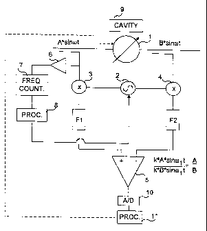
FIG. 1 shows a block diagram of an embodiment of the invention;
FIG. 2 shows a diagram of a) an input to the resonance module during a time
gap,
b) the output from the resonance module during the same time gap, and c)
to the output from the dual channel measurement receiver during the same
time.
DETAILED DESCRIPTION OF EMBODIMENT
1s Referring to FIG. 1, a resonance module 1 is fed with an incoming signal
A*sinc~t. The
resonance module is to be tuned such that it provides an output B*sinwt. The
tuning is
provided by deriving both the input and the output of the resonance module. A
high-
frequency oscillator 2 is controllable and has a frequency range in which the
input
signal to the resonance module 1 lies. An input signal mixer 3 mixes the
derived input
2o signal to the module 1 with the frequency of the oscillator 2 in order to
have a
frequency offset in relation to the derived frequency, which is high. An
output mixer
mixes the derived output signal from the module 1 with the frequency of the
oscillator
2.
2s The output of the input mixer 3 is fed, via a first amplifier and filter F
l, which makes a
channel filtration and which can make a low-pass or a band-pass filtration, to
a first
input of a dividing unit 5. The output of the output mixer 4 is fed, via a
second filter
and amplifier F2, which can make a low-pass or a band-pass filtt-ation, to a
second
input of the dividing unit 5. The dividing unit 5 provides the ratio between
the inputs
CA 02361369 2001-07-23
WO 00/45512 PCTlSE00/00164
s
of the dual channel measurement receiver, i.e. the input and the output of the
resonance module 1.
The input and output signals are thus to be compared with each other. Thus
s (k*Asinwlt)/(k*Bsinwlt) = AB is the attenuation caused by the resonance
module, the
index '1' is used because the signals now have been mixed by the mixers 3 and
4,
respectively. Also, the signals are proportional to the derived signals, which
is
indicated by the constant k. The resonance module 1 can then be tuned by the
output
of the dividing unit 5 so that a kind of bathtub-curve is received having its
minimum
io attenuation at the tuned frequency.
The output of the dividing unit 5 is therefore analogue/digital converted in
an A/D
converter 10 and fed to an adjustment device l 1 which calculates the tuning
procedure,
i.e. the tuning direction, and tunes the resonance module 1 in a reciprocating
way, by
1s adjusting stepping motors in the way well known for a person skilled in the
art, until
the output of the unit 5 has a minimum. Then the signal will be independent of
the
momentary actual power of the signal. It is to be noted that the relationships
stated
above will fit better when the tuning approaches the con-ect tuning value.
2o The kind of modulation has no influence on the signal transfer since there
is only a
signal ratio. The output of the resonance module 1 thus has the same form as
its input.
There is in fact a small time delay between the output and the input but this
delay is
very small in relation to the modulation changes and is filtered away using a
low-pass
filter at the output side of the resonance module.
2s
The power of the input to the resonance module 1 is detected by a circuitry
comprising
an amplifier 6, a frequency counter 7 to make a fi~eduency division of the
input signal
and a processing unit 8 which calculates the power and the frequency to which
the
resonance module 1 is to be tuned. The output of the processing unit 8 is fed
to an
3o input of the frequency generator 2 to adjust the generator to the centre
frequency of the
CA 02361369 2001-07-23
WO 00/45512 PCT/SE00/00164
6
filters F1 and F2 in relation to the actual frequency channel. It is to be
noted that a lot
of channels (for instance 8, 12, 16, 32 etc. channels) are adjustable
separately in this
way.
s Thus, by implementing a dual channel measurement receiver which measures
both the
input and output of the resonance module 1 coherently and computes the
difference
between the signals it is possible to deduce a signal which is proportional to
the
attenuation of a cavity 9. Any influence of the modulation scheme will be
suppressed
since the output of the module 1 is the ratio of both the input and the output
of the
io module, i.e. both inputs to the dual channel receiver, independently of any
modulation
wave-form. Hence the performance of the auto-tuning can be improved
significantly
by the inventive measurement receiver in relation to prior art receivers.
This means also that the dual channel measurement receiver controls itself,
i.e. is auto-
~s controlled, and thus need not be controlled from another system. This kind
of receiver
does not need any calibration of the wiring etc. The dual channel measurement
receiver can also handle the modulation type in the actual band width of the
measurement receiver. The unit 5 produces the ratio between the derived
signals from
each side of the resonance module 1. The influence of the power changes, i.e.
the
2o modulation of the signal on each side of the resonance module, cancel each
other, and
it is easy for the processing means 11 to find the optimal tuning by tuning
the
resonance module 1 in small steps until the output of the unit 5 has reached a
minimum.
2s The circuitry according to the invention could also be used to measure the
power of the
input signal and the output signal of the resonance module separately by
deconnecting
the one or the other of the deriving circuits. The output of the deriving unit
5 will then
have a value in relation to the signal to be separately measured. This feature
makes the
dual channel measuring receiver still more useable.
CA 02361369 2001-07-23
WO 00/45512 PCT/SE00/00164
FIG 2 shows diagrams recorded at a test with the circuihy according to the
invention
where the curve a) shows an input to the resonance module during a time gap,
b) the
output from the resonance module during the same time gap, and c) the output
from
the dual channel measurement receiver during the same time. The test were made
after
that the tuning of the resonance module 1 was finished. It is apparent that
the effect of
the signal variation is canceled so that only unavoidable noise on the signals
is left in
the output of the unit S.
While the invention has been described with reference to specific embodiments,
it will be
~o understood by those skilled in the ait that various changes may be made and
equivalents
may be substituted for elements thereof and different featw-es described for
one
embodiment could be adequate also in the other embodiments without departing
from the
true spirit and scope of the invention as it is stated in the claims on file.
In addition,
modifications may be made without departing fi-om the essential teachings of
the invention
is as apparent from the claims.