Note: Descriptions are shown in the official language in which they were submitted.
* .` I
CA 02361519 2001-07-27
- 1 -
DESCRIPTION
OPTICAL ELEMENT SUCH AS MULTILAYER FILM REFLECTOR,
AND THE LIKE, METHOD OF MANUFACTURING THE SAME,
AND APPARATUS USING THE SAME
TECHNICAL FIELD
The present invention relates to an optical element such
as a ref lector, and the like making use of ref lection by amultilayer
film, and more particularly, to the correction of a wavefront
phase of rays emerging from a multilayer film reflector.
BACKGROUND ART
Fig. 1 shows a relationship between the classification of
electromagnetic waves and wavelengths thereof. First, extreme
ultraviolet rays and X-rays will be described with reference to
Fig. 1. Extreme ultraviolet rays (EUV) and vacuum ultraviolet
rays ( N~UV ) are electromagnetic waves having a wavelength shorter
than that of ultraviolet rays in the classification of the
electromagnetic waves shown in Fig. 1(a). As can be seen from
the comparison of the classification of the electromagnetic waves
of Fig. 1(a) with the wavelengths of electromagnetic waves of
Fig. 1(b), X-rays indicate electromagnetic waves having a
wavelength of 0.001 to 50 nm, wherein soft X-rays indicate X-rays
having a wavelength of 0.5 to 50 nm. While a boundary between
CA 02361519 2001-07-27
=
_ 2 -
extreme ultraviolet rays and vacuum ultraviolet rays and soft
X-rays is not clearly determined and they are partly overlapped
in the classification, extreme ultraviolet rays, vacuum
ultraviolet rays,andsoft X-rays are electromagnetic waves having
an intermediate wavelength of the wavelengths of ultraviolet rays
and hard X-rays. Extreme ultraviolet rays, vacuum ultraviolet
rays, and soft X-rays have such a property that they have a small
amount of transmittancy and absorbed by an air layer. However,
since they have a particularly high photon energy, they exhibit
a transmittance force which permits them to penetrate the interior
of a material such as metal, semiconductor, insulator, and the
like from the surface thereof by several hundreds of nanometers.
Further, since soft X-rays have such a degree of a photon energy
as to be absorbed in inner shell electrons of atoms constituting
a material, they exhibit an apparent difference of absorption
depending upon elements constituting various materials. This
property of soft X-rays is most suitable to the study of various
type ofematerials together with the high resolution thereof. Thus,
soft X-rays contributes to the study and development of an X-ray
microscope capable of observing living specimens as they are
without drying and dyeing them.
Extreme ultraviolet rays (vacuum ultraviolet rays) and
X-rays have a high photon energy as compared with that of visible
rays and have a high transmittance force to materials. Since
extreme ultraviolet rays and X-rays are not refracted in almost
CA 02361519 2001-07-27
- 3 -
all the materials because of the above reason, it is difficult
to make a lens . Accordingly, while reflectors are used to converge
extreme ultraviolet rays and X-rays and to form images using them,
even a metal surface does not almost reflect extreme ultraviolet
rays and X-rays. However, since the metal surface can reflect
extreme ultraviolet rays and X-rays when they are incident on
it at an angle almost close to the metal surface, an optical system
making use of the oblique incidence could not held being employed.
Thereafter, a great deal of attention was paid to a
"multilayer film mirror" capable of reflecting extreme
ultraviolet rays (vacuum ultraviolet rays ) or X-rays including
soft X-rays, which opened a way for developing an optical system
in which these rays were incident at near normal angle on an extreme
ultraviolet ray and X-ray imaging optical system. An X-ray
micrometer making use of X-rays employs the above-mentioned
multilayer film mirror. The multilayer film mirror will be
described with reference to Fig. 2.
Fig. 2 (a) shows construction of the multilayer film mirror,
and Fig. 2(b) shows construction of a reflective film. In Fig.
2( a), the multilayer film mirror is composed of a multilayer film
20 formed on a substrate 10, and Fig. 2(b) shows an example of
construction of a multilayer film used to soft X-rays having a
wavelength of about 13 nm (photon energy: 9 7 eV ). In Fig. 2( b),
the multilayer film 20 is composed of several tens to several
hundreds of layers each including a pair of molybdenum (Mo) and
CA 02361519 2001-07-27
- 4 -
silicon(Si). The multilayerfilm20is attached to the substrate
as shown in Fig. 2(a). A normal incidence reflectance of 60%
can be obtained by the multilayer film mirror constructed as
described above.
Fig. 3 shows an example of a schematic construction of an
X-ray apparatus using the multilayer film reflector shown in Fig.
2(a). In Fig. 3, the X-ray apparatus is composed of two ref lectors,
that is, a reflector having the reflective multilayer film 20
attached to the substrate 10 having a concave surface and a hole
defined at the center thereof and a reflector having a reflective
multilayer film 22 attached to a substrate having a concave surface
similarly. Reference symbol L denotes X-rays and the light path
thereof.
When X-rays are irradiated toward a body 30 from the left
side in Fig. 3(a), the X-rays L are reflected by the multilayer
film reflectors 20 and 22, and an enlarged image 35 of the body
can be obtained. At that time, the apparatus stiown in Fig. 3(a)
achieves a role as a microscope as shown in (1) of Fig. 3(b).
The image is formed by X-rays the wavelength of which is one several
hundredth or less those of visual rays and ultraviolet rays, which
can improve the accuracy of even a very f ine body making the limit
of resolution caused by unsharpness due to diffraction to one
several hundredth or less in principle. The above technology
is further grown to the development and study of an X-ray telescope
of high accuracy, which contributes to the investigation of the
CA 02361519 2001-07-27
- 5 -
origin of the Milky Way and structures of supernovas by the
observation of soft X-rays generated f rom ultra-high temperature
plasmas.
Further, when X-rays are irradiated toward the body 35 from
the right side in Fig. 3(a), the X-rays L are reflected by the
multilayer film reflectors 22 and 20 so that a reduced image 30
of the body comes out. At that time, the apparatus shown in Fig.
3(a) is constructed as an exposing apparatus for executing
micro-focusing and reduction as shown (2) of Fig. 3(b).
Competition for developing an X-ray multilayer film mirror for
a reduced projection exposure optical system is carried out
internationally mainly by United States and Japan to use the X-ray
multilayer film mirror as a central component of a next-generation
ultra LSI manufacturing apparatus.
As described above, the application of the X-ray multilayer
film mirror to various fields is expected not only by industrial
circles but also by academic circles.
~hese X-ray multilayer film mirrors must be provided with
a wavefront accuracy of at least one eighth or less a wavelength
to obtain an imaging performance. To achieve this value,however,
it is indispensable to finally develop a method of measuring and
correcting an wavefront error at a wavelength of X-rays being
used, in addition to the developments of a method of measuring
and controlling an accuracy of shape of a spherical substrate,
a method of forming a multilayer f ilm, which has a high ref lectance
CA 02361519 2001-07-27
- 6 -
and applies no distortion to a substrate, on the substrate, a
method of holding an imaging mirror without distortion, a method
of adjusting the imaging mirror, and the like.
In particular, the method of correcting a wavefront
aberration which is definitely important to the determination
of a final imaging performance is encountered with difficulty
because an amount of correction is the order of nanometers. At
present, an adaptive optics (compensation optical) system for
minutely deforming a substrate at an accuracy of nanometers by
driving a piezo element and the like, and a method of applying
a thin f ilm to the surf ace of a substrate or ion etching the substrate
are proposed.
For example, there is a trial for adaptively correcting
a shape of a reflector by an actuator. This trial will be explained
by a wavefront aberration correcting apparatus shown in Fig. 4.
As shown in Fig. 4, the wavefront aberration correcting apparatus
corrects a wavefront by correcting a shape of the:multilayer film
mirror}20 by applying force to the substrate 10 by an actuator
60 attached to the substrate 10 of a ref lector. In the correcting
apparatus, soft X-rays L passing through a pinhole 110 is introduced
to the reflector by a beam splitter 120 and reflected by the
multilayer film mirror 20. In the above construction, when a
knife edge 130 is inserted into the light path of the soft X-rays
L passing through the beam splitter 120, a shape of a mirror surface
can be measured by analyzing an image projected onto a
CA 02361519 2009-05-07
7
two-dimensional detector 150 with a computer 160. The shape of the reflector
is
corrected by operating the actuator 60 by a control circuit 170 based on a
result
of the measurement.
However, these methods are encountered with a great deal of difficulty
because they are inevitably required to measure and control a very minute
amount of 1 nm or less to geometrically and optically control a reflection
surface
in principle.
DISCLOSURE OF INVENTION
An object of an aspect of the present invention is to provide an optical
element such as a multilayer film reflector and the like having a structure
capable
of simply correcting a wavefront phase.
To achieve the above object, according to an aspect of this specification,
an optical element for controlling a phase and an amplitude of emerging rays
by
a multilayer film, comprising a substrate having an error of shape; and a
multilayer film formed on the substrate and reflecting radiation in a range
from
vacuum ultraviolet through X-ray, wherein at least one cycle of a
predetermined
portion of the multilayer film corrects a wavefront aberration of a wavefront
phase
of a light reflected by the multilayer film that would have been caused by the
error
of shape of the substrate if said at least one cycle did not make a
correction.
The formation of correction film as well as the formation of a multilayer
larger than necessary to substantially saturate the reflectance permits the
correction of a phase by cutting away also the multilayer film when the phase
cannot be corrected only by cutting way the correction film, whereby the phase
can be corrected more accurately.
CA 02361519 2009-05-07
8
The use of the above-mentioned multilayer film reflector in a microscope,
an exposing apparatus, a telescope, a microprobe, an analyzer and the like for
X-rays and extreme ultraviolet rays (vacuum ultraviolet rays) permits a
difference
of phase to X-rays and extreme ultraviolet rays (vacuum ultraviolet rays) to
be
controlled by cutting away the multilayer film and the like, whereby a desired
imaging performance can be easily obtained.
According to another aspect, an optical element forming method is set
forth comprising forming, on a substrate having an error of shape, multilayer
film
stack of alternating layers that reflects radiation in a range from vacuum
ultraviolet through X-ray; and cutting away at least one cycle of alternating
layers
from a portion of the multilayer film stack so that the multilayer film stack,
having
said at least one cycle cut away, corrects a wavefront aberration of a
wavefront
phase of a light reflected by the multilayer film stack that would have been
caused by the error of share of the substrate if said at least one cycle of
alternating layers were not cut away.
According to yet another aspect, an optical element forming method,
comprising forming a multilayer film on a substrate in a number of cycles
larger
than that necessary to saturate a reflectance; forming a correction film on
the
multilayer film; and cutting away a portion of the correction film or a
portion of the
correction film and a portion of the multilayer film in accordance with an
amount
of adjustment of a wavefront phase of emerging rays.
BRIEF DESCRIPTION OF THE DRAWINGS
Fig. 1 is a view showing a classification of electromagnetic waves and
wavelengths of electromagnetic waves;
Fig. 2 (a) is a view showing construction of a multilayer film mirror, and
Fig. 2 (b) is a view showing a Mo-Si multilayer film;
Fig. 3 is a view showing a schematic construction of an X-ray apparatus
using a multilayer film reflector;
CA 02361519 2009-05-07
8a
Fig. 4 is a view showing a wavefront aberration correcting apparatus for
correcting a wavefront by correcting a shape of a multilayer film mirror by
applying force to a substrate by an actuator;
Fig. 5 is a graph showing a reflectance when a number of multilayer films
for executing reflection is increased;
Fig. 6 is graph showing a change of a phase and a reflectance when the
multilayer films which larger than that necessary to
CA 02361519 2001-07-27
= - 9 -
saturate the reflectance are removed;
Fig. 7 is a view showing construction of a multi-layered
mirror of another embodiment of the present invention;
Fig. 8 is a view showing procedures for correcting the
multilayer film mirror of the another embodiment;
Fig. 9 is a graph showing a case in which an auxiliary film
and the multilayer film which has the number of cycles larger
than that necessary to saturate a reflectance are cut away;
Fig. 10 is a view showing construction of a soft X-ray
microscope system using the multilayer film of the present
invention; and
Fig. 11 is a view showing construction of a soft X-ray
telescope system using the multilayer film of the present
invention.
BEST MODE OF CARRYING OUT THE INVENTION
Embodiments of the present invention will be described below
in dettil with reference to the drawings.
Fig. 5 is a graph showing a relationship between the number
of cycles as the number of films of a multilayer films (number
of repetitions of films constituting the reflective multilayer
film, each of the films being composed of a material having a
high refractive index and a material composed of a material having
a low refractive index) and a reflectance in a reflector using
a multilayer film as shown in Fig. 2( a) . The films have an optical
CA 02361519 2001-07-27
- 10 -
thickness of one fourth a wavelength, respectively. Fig. 5 shows
a relationship between a multilayer film composed of ruthenium
( Ru ) and silicon ( Si ), a multilayer f ilm composed of rhodium ( Rh )
and silicon (Si), a multilayer film composed of molybdenum (Mo)
and silicon (Si), a multilayer film composed of ruthenium (Ru)
and carbon (C), and a multilayer film composed of rhodium (Rh)
and carbon(C) and reflectances.
As can be seen from the graph shown in Fig. 5, an increase
in the number of cycles of the films constructing the multilayer
film causes the reflectance to saturate so that the reflectance
is not changed even if the films are repeated.
A saturated reflectance does not reach 100% and takes a
value of about 15% to 80% in a wavelength region in which film
materials that absorb extreme ultraviolet rays, soft X-rays,
X-rays, and the like are used as an element of the multilayer
film. In this saturated state, a multilayer film formed in the
number of cycles larger than that necessary to saturation changes
the phase of reflected rays while it does not contribute to an
increase in an amplitude.
Therefore, a wavefront phase can be corrected by forming
a multilayer film the number of cycles of which is larger than
that necessary to substantially saturate a reflectance and by
cutting away the multilayer film in the range in which the
reflectance is saturated because of a reason described below.
That is, several tens to several hundreds of layers of lamination
CA 02361519 2001-07-27
- 11 -
is necessary in a multilayer film mirror used for, for example,
X-rays, and extreme ultraviolet rays (vacuum ultraviolet rays)
because a very minute amount of ref lection is caused on respective
boundaries. According to a theoretical analysis, reflection is
caused on an overall multilayer film physically and optically.
Therefore, the surface portion of the multilayer film acts as
a transmission film.
The present invention corrects the wavefront phase of
emerging rays by forming a multilayer film having the number of
cycles which is larger than that by which a reflectance is
substantially saturated and by cutting away the multilayer film
in accordance with an amount of adjustment of the wavefront phase.
When the amount of correction is relatively small, the phase can
be corrected by cutting away the multilayer film so that the
variation of a reflectance can be reduced as compared with a case
in which the multilayer film is formed by adding a correction
film as described below.
~ig. 6 shows an example in which changes of a phase and
a reÃlectance are measured by cutting away a multilayer f ilm formed
in the number of cycles larger than necessary to saturate the
reflectance. Soft X-rays measured have a wavelength of 12.78
nm, and the multilayer film is composed of Mo/Si, has a thickness
one fourth a wavelength and is formed of 121 layers. Complex
refractive indices nsi and nMo of silicon ( Si ) and molybdenum (Mo)
that form the multilayer to the soft X-rays having the wavelength
CA 02361519 2001-07-27
- 12 -
of 12.78 nm are as follows.
nsi = 1.00276 - 0.0015i
nMo = 0.9324 - 0.00598i
A reflectance by the multilayer film is 76.4%. Fig. 6 shows a
change of a phase (a) and a change of a relative reflectance ( b),
respectively when the multilayer film is cut away from the upper
portion thereof. As can be seen from the graph, even if the
multilayer film, which is formed in the number of cycles larger
than that necessary to saturate a reflectance, is cut away, the
reflectance is not changed, but the phase of reflected rays is
changed.
A step at which the phase is changed in Fig. 6 is caused
by milling (cutting away) one cycle of the multilayer f ilm. That
is, the phase is changed in such a manner that it is reduced by
milling a Mo film and slightly increased by milling a Si film.
Since each layer of the Mo/Si multilayer film shown in Fig. 6
has a film thickness of about 4 nm, milling of one Mo layer
corresvonds to the reduction of a phase angle of 5 . When this
value is shown as an error of shape of a substrate, it corresponds
to (13 nm/2) *(5 /360 ) = 0.09 nm, which shows that the error
of shape of the substrate can be digitally controlled by 0.9A
by milling one cycle of the film. In other words, when it is
intended to mill a predetermined portion of a surface in a certain
amount of correction, a milling thickness can be precisely
controlled by stopping milling when a material appearing on the
CA 02361519 2001-07-27
- 13 -
surface is changed from Mo to Si.
A change of a material caused by milling can be simply
monitored using a method of monitoring a material discharged by
milling, an electronic method of utilizing a change of a material
in a secondary electron discharge yield, a reflectance measuring
method utilizing an optical change of characteristics such as
a change of an optical constant of visible rays, ellipsometry,
and the like. These methods can be easily used together with
a most ordinary method of controlling a milling depth by a
cutting-away time by stabilizing an amount to be cut-away in time.
These features result from that the phase is corrected by milling
at least one cycle of the surface of the multilayer film.
It has been described above that when milling is carried
out for each one cycle in the example of the Mo/Si multilayer
film shown in Fig. 6, an accuracy of 0.1 nm can be achieved to
the error of shape of the substrate. However, when the milling
of one cycle is examined in detail, the following steps can be
found: -
1. the phase is not almost changed in the milling of the
Si layer (actually, the phase is slightly increased because a
refractive index is slightly larger than 1);
2. at the same time, a relative intensity reflectance is
in a flat state in which it is not almost changed while the Si
layer is being milled (the bottomportion of a change of oscillation
due to interference); and
= CA 02361519 2001-07-27
- 14 -
3. in contrast, the phase is reduced and the reflectance
is changed while the Mo layer is being milled.
Accordingly, when milling is stopped at the portion of each Si
film in the above digital milling, only the phase is changed by
a predetermined angle (about 6 ) each time, and the reflectance
is not changed. Specifically, since it is sufficient to stop
milling when Si appears by milling a Mo layer, a timing at which
milling is stopped has a large amount of allowance. Specifically,
when a Si film has a thickness within the range of about 3.5 nm,
it has an allowance of at least +1 nm. Further, a change of the
reflectance can be easily made within 1% making use of this
property.
Incidentally, when a complex amplitude reflectance of a
multilayer film is taken into consideration on a complex plane,
a radius vector is equal to an amplitude and an angle of deviation
is represented by the same point. Therefore, cutting-away of
the multilayer film causes the complex amplitude reflectance to
move on;a circumference the center of which substantially coincides
with an origin.
Theoretically, when a change of an amplitude reflectance
is determined in the cutting-away of a multilayer film from the
upper surface thereof, a reference of calculation of a phase and
an amplitude resides on the uppermost surface of the multilayer
film at all times. Thus, it is necessary to use the surface of
the multilayer film before it is cut away as the reference surface
CA 02361519 2001-07-27
- 15 -
of the phase to calculate an effect for cutting a certain portion
from the surface. To satisfy this object, it is necessary, when
a certain thickness d is cut away, to calculate the effect by
assuming that a vacuum layer is laminated by the thickness d:
This assumption makes it possible to fix the reference surface
fixed at a position prior to cutting-away at all times so that
the effect of a predetermined phase and a predetermined amplitude
obtained by the cutting-away can be precisely calculated.
Fig. 7 shows another construction of a reflector of the
present invention. In Fig. 7, a correction film 50 is formed
on a multilayer film 20 which is formed on a substrate 10 in the
number of cycles larger than that necessary to saturation.
In a multilayer film mirror used for, for example, X-rays
and extreme ultraviolet rays (vacuum ultraviolet rays), several
tens to several hundreds of layers of lamination are necessary
because a reflection is caused very slightly on respective
boundaries. According to a theoretical analysi-s, reflection is
caused-on an overall multilayer film physically and optically.
Thus, as shown in Fig. 7, the addition of the phase correction
film 50 on the uppermost surface of the multilayer film 20 larger
than substantial saturation permits the film 50 to act as a
transmission phase correction film. However, since no
transparent material exists in this wavelength region, a material
which can constitute the phase correction film must satisfy the
condition of an extinction coef f icient k together with a ref ractive
= CA 02361519 2001-07-27
- 16 -
index n.
A film material constituting the correction film can provide
a larger amount of phase correction when it has a larger difference
between refractive indexes (1 - n) and a smaller extinction
coefficient k. Therefore, an optical reference for selecting
a material can be judged by a ratio between an amount of change
of a phase caused by a unit thickness and damping of an amplitude
caused by absorption, and a suitable material has a lager value
of {difference between refractive indexes (1 - n)/extinction
coefficient k}.
When soft X-rays having a wavelength of 13 nm is used as
an example, the use of molybdenum (Mo) film, in which a difference
(1 - n) between a refractive index n of the film and a refractive
index 1 of vacuum in a soft X-rays region is about 0.1 or less
(difference between refractive indexes: 0.065, extinction
coef f icient: 0. 0065 ) permits a f ilm thickness to be geometrically
controlled at a resolution of about 1/15 because a difference
of a phase is physically optically controlled in a difference
between refractive indexes (1 - n) of about 1/15. That is, an
effective wavefront control of 1 nm of an X-ray multilayer film
imaging mirror can be achieved by the control of the molybdenum
film having a film thickness of 15 nm, and a desired imaging
performance can be obtained. Thus, it is sufficient to cut away
the correction film at an accuracy of 1.5 nm of a film thickness
to correct a phase error at an accuracy of 0.1 nm because the
CA 02361519 2001-07-27
- 17 -
amount of correction is a product of the difference between
refractive indexes (1 - n) and the amount of change Ad of the
film thickness d.
Further, a change of reflectance caused by a correctiori
film must be calculated in consideration of a change of film
thickness and interference of a multilayer film. However, a
reduction rate of reflectance is about 1.2%/nmeven if it is simply
calculated and it is reduced only by about 0.7$ in a mirror having
a reflectance of 60%.
When sufficient correction cannot be performed by the
correction film, correction can be further carried out by cutting
away the multilayer f ilm larger than that necessary to substantial
saturation.
Ruthenium, rhodium, and beryllium are available as the
material having a large difference between refractive indexes
(1 - n) and a small extinction coef f icient k. A correction film
to soft X-rays can be composed of one of these materials including
molybdenum or a combination of these materials.
Fig. 8 explains a method of correction using the correction
film and the multilayer film shown in Fig. 7.
As shown in Fig. 8(a), the correction film 50 having a
sufficient thickness is previously formed on the multilayer film
20 that is formed on the substrate 10, and the correction film
50 is cut away by milling in a necessary amount (refer to Fig.
8(b)). When the correction film 50 cannot be sufficiently cut
,
CA 02361519 2001-07-27
- 18 -
away, the multilayer film is cut away (refer to Fig. 8(c)).
While the uppermost surface of the correction film and the
like having been milled by the method is roughened, a transmission
wavefront is not almost affected by the roughness because the
difference of the refractive index thereof to vacuum is small.
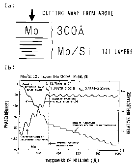
Fig. 9 is a graph showing an example that after a multilayer
film was formed in the number of cycles which was larger than
that necessary to substantial saturation and a correction film
was formed thereon, the correction film and the multilayer film
were cut away from the upper portions thereof as explained in
Figs. 7 and 8, and a change of wavefront phase was measured. As
shown in Fig. 9(a), after 121 cycles of a Mo/Si multilayer film
was formed and a molybdenum (Mo) correction film of 300 A was
formed thereon, the Mo correction filmwas cut away from the upper
portion thereof. A complex refractive index of silicon ( Si ) nsi
and a complex refractive index of molybdenum (Mo) nMo that formed
the multilayer film to soft X-rays having a wavelength of 12.78
nm werV as follows.
nsi = 1.00276 - 0.0015i
nMa = 0.9324 - 0.00598i
Further, a reflectance of the 300 A correction film and the
121-multilayer film was 56.2%.
Fig. 9(b) shows a case in which the correction film and
the multilayer film constructed as described above were cut away
from the upper portions thereof. Fig. 9(b) shows a relative
CA 02361519 2001-07-27
= - 19 -
reflectance to the soft X-rays having the wavelength of 12.78
nm (which is 1 when they are not cut away: shown on a right scale)
and a change of wavefront phase (which is 0 when they are not
cut away: shown on a left scale). When the correction film is
cut away, the phase and the reflectance are not changed linearly
and are variably changed by the interference of the Mo film.
Further, when the multilayer film is cut away, the cycles of change
of the phase and the reflectance coincide with the cycles of the
cyclic film. A change of reflectance, when the multilayer film
portion is cut away, is small as compared with a change thereof
when the correction film is cut away.
As can be seen from the graph of Fig. 9(b) showing the
correction film having been cut away, the phase can be changed
by cutting away also the multilayer film. However, an amount
of correction of phase to a cut-away amount, which can be achieved
by cutting away the multilayer film, is smaller that achieved
by cutting away the correction film.
<Example of use of reflector>
Fig. 10 shows a soft X-ray microscope system using the
above-mentioned reflector capable of simply correcting a
wavefront error. A light path of soft X-rays is disposed in a
vacuum vessel 2 0 0 because soft X-rays are absorbed by air. Further,
the system is roughly divided into four components of a light
source, an imaging optical mirror, a detection subsystem, and
a control/measurement subsystem, and can observe a specimen 310
CA 02361519 2001-07-27
- 20 -
using these components.
A laser generator 210, a metal target 300, a spectroscope
220, and a pin hole 230 are used as the soft X-ray source. The
imaging optical mirror 240 is composed of a combination of the
above-mentioned multilayer film mirror, which has a concave
surface and a hole defined at the center thereof, and the
above-mentioned multilayer film mirror having a convex surface
and disposed just in front of the above multilayer film mirror.
The microscope system further includes a two-dimension detector
250 and a computer 260. The two-dimension detector 250 has a
photoelectric surface 252 for detecting the soft X-rays irradiated
to the specimen 310, and the computer 260 captures detected data
and controls a position of the specimen.
In this construction, first, when strong infrared pulse
laser is converged at the metal target 300 by the pulse laser
generator 210 through a lens to generate soft X-rays as a light
source, plasma having a high energy is generated. The plasma
emits Tlectromagnetic waves having various wavelengths. Thus,
soft X-rays are taken out from the electromagnetic waves having
the various wavelengths using the spectroscope 220. The soft
X-rays emerging from the spectroscope 220 pass through the pin
hole 230 and irradiates the specimen 310. The soft X-rays
irradiated to the specimen 310 enlarge the image of the specimen
310 by the imaging optical mirror 240 and form it on the
photoelectric surface252of the two-dimension detector250. Then,
CA 02361519 2001-07-27
- 21 -
the computer 260 captures the data detected by the two-dimension
detector 250 and forms it as an image. The computer 260 also
controls a position of the above-mentioned specimen 310, in
addition to the above.
The use of the above-mentioned construction in the ref lector
used in the microscope system as described above can correct a
wavefront aberration of rays at an accuracy and a resolution of
1 nm or less. With this construction, an optimum wavefront
accuracy can be obtained in accordance with a state in which the
reflector is used by finally correcting an X-ray wavefront using
a correction film and the like after a multilayer film is formed
even if an error of shape of a substrate does not reach a desired
value.
In the application of the reflector to an X-ray telescope,
a telescope of a directly incident Cassegrainian telescope and
the like of light weight and high performance can be constructed
in place of a nested-type telescope having an obliquely incident
cylindrical mirror as a nest by employing correction executed
by the correction film and the like. Fig. 11 shows an example
of construction of the telescope.
In Fig. 11, a reflective type telescope 400 is mounted on
a camera 450. The multilayer film reflector described above is
used in each of ref lectors 410 and 415 constructing the ref lective
type telescope 400. After rays incident on an outside cylinder
420 are reflected by the reflector 410, they are reflected by
= CA 02361519 2001-07-27
- 22 -
the reflector 415 and incident on the camera 450 from a baffle
430.
With this construction, an ultimate resolution as small
as an aproximate observing wavelength, which cannot be obtained
by a conventional telescope, can be expected in an X-ray telescope
of light weight and high performance, which is mounted on, for
example, an artificial satellite, by reducing a wavefront
aberration of a multilayer film mirror.
The above-mentioned multilayer film reflector can also be
used in an X-ray microprobe. In the application of the multilayer
film reflector to the X-ray microprobe, a special resolution,
which is conventionally several tens of micrometers, can be reduced
up to the region of 0.01 m, which can dramatically widen subjects
to be inspected by the X-ray microprobe including various types
of submicron devices.
The above-mentioned multilayer film reflector can be used
also in an X-ray analyzer. The X-ray analyzer; can improve an
angle accuracy as well as can observe a minute specimen because
it can collimate beams parallel or converge them. Further, the
multilayer film reflector can be applied to the analysis of a
two-dimensional image by being combined with an imaging system.
Defects made on a reflective wavefront can be repaired in
a multilayer film reticle mask and an imaging mirror used in a
reduced projection exposure optical system, in addition to the
above-mentioned X-ray microscope, X-ray telescope, X-ray
CA 02361519 2001-07-27
- 23 -
microproble, and X-ray analyzer.
Since the wavefront of the multilayer film mirror can be
easily corrected in the various applications of the X-ray
transmission multilayer f ilm in addition to the above, the phase
of X-ray transmission and reflection wavefronts can be adjusted
to target values and target two-dimensional distributions.
While the application of the multilayer film reflector to
the equipment using X-rays is described above, it is needless
to say that the multilayer film reflector can also be used in
equipment using extreme ultraviolet rays (vacuum ultraviolet
rays), and the like in the same way. Further, since the principle
of the present invention utilizes the physical and optical
properties of rays, the present invention is effective to all
the electromagnetic waves making use of a multilayer film such
as ultraviolet rays, visible rays, infrared rays, and further
a microwave region, and the like. For example, in the application
for increasing an accuracy of a reflective wavefront, the present
invention is very effective to a mirror for a laser oscillator
and to a mirror constructing similar Fabry-Perot and ring laser
gyro resonators. Further, since it is possible to provide special
wavelength dispersion characteristics making use of a diffractive
effect, a polarizing element having wavelength dispersion can
be made by the utilization of polarizing characteristics
accompanying with the special wavelength dispersion
characteristics. Thus, the polarizing element can be used in
CA 02361519 2001-07-27
- 24 -
a mirror and a beam splitter. In particular, the polarizing
characteristics are effective to a half mirror of a photomagnetic
apparatus.
It is also possible to make a phase grating using the
multilayer film of the present invention. In the formation of
the phase grating, a groove structure having a thickness for
providing a phase difference of 180 is formed on the surface
of a substrate using the multilayer film. The phase grating is
a diffraction grating of a new type that acts as a two-dimensional
phase grating. In a conventional method, since the surface of
a substrate is roughed due to a groove structure formed on the
substrate, the characteristics of a multilayer film formed on
thesurface is deteriorated. Further, a processing accuracy must
be kept to at least one-twentieth or less a wavelength to be used.
The method of the present invention can achieve an accuracy,
which cannot be achieved by a conventional geometrical reflective
surface position control, by controlling a difference of light
path. 4The difference of light path is a product of a milling
thicknessdof amultilayer filmandadifferencebetweenrefractive
indexes (n - 1). The difference of reflective indexes is a
difference between an average refractive index n of a multilayer
film and a refractive index 1 of vacuum (medium). A smaller value
of ( n- 1) increases an accuracy of a wavefront which is corrected
by milling a thickness d. When visible rays are used in a
transparent material such as a glass, improvement in accuracy
CA 02361519 2001-07-27
- 25 -
is doubled (1.5 - 1= 0.5), whereas, in a soft X-ray region,
improvement of accuracy of the order of one hundred times is
expected because a refractive index is slightly smaller than 1
and (1 - n) is the order of 0.01.
Further, the multilayer film of the present invention can
be used as an amplitude modulation hologram. In this case, the
hologram is formed by cutting away the multilayer film by two
dimensionally controlling a surface shape in a plane so as to
regulate the phase and the amplitude of a wavefront from which
rays emerge.
An element which can be used to f ilter a phase and an amplitude
can be formed by forming the multilayer film of the present
invention. In this case, a novel means for executing various
types of filtering in a spatial frequency space is provided by
combining the multilayer film with an imaging system.
The present invention can provide a new method of realizing
a novel image display panel and the like by further modulating
an opt~cal length (length of a light path) in time in the above
method. Further, the multilayer film can be used as a transmission
type multilayer film because it substantially acts as a
transmission f ilmwith respect to reflection from a lower portion.
In addition to the above-mentioned, when such a
characteristic that a refractive index is greatly different
depending a wavelength is utilized, an element can be made which
makes use of a phenomenon that a different surface shape appears
CA 02361519 2001-07-27
- 26 -
depending upon a length of rays. For example, an mirror used
for extreme ultraviolet rays ( EUV ) has an ideal shape (for example,
spherical shape) to EUV rays. However, since the spherical
surface shape disappears after a wavefront is corrected, the mirror
has such characteristics that rays reflected on the surface of
the mirror are, for example, diverged apart from the spherical
surface. That is, a different refractive index can provide
characteristics which are similar to a case in which a surface
shape is changed depending upon a wavelength. This permits a
mirror to be made which has such a feature, for example, that
while rays having a certain wavelength is converged by the mirror,
rays having other wavelength are not converged thereby. When
this feature is applied to an imaging system, an optical system,
in which an image can be formed sharply by rays having a certain
wavelength but an image formed by rays of other wavelength is
made unsharp. On the contrary, when the rays are stopped at a
converging point, an image is formed by rays fromwhich a certain
wavelength is removed. This means that a reflector having a very
large amount of color aberration can be made in, for example,
a transmission optical system. When this feature is developed,
an element, which positivelymakes use of dispersion of awavelength
of a refractive index, such as a mirror having a different focal
length depending upon a wavelength, a double focus mirror, and
the like can be realized. A refractive index is only slightly
dispersed in a conventional transmission optical element because
CA 02361519 2001-07-27
- 27 -
the element makes use of a transparent material, that is, a material
in which a refractive index is normally dispersed. Thus, the
element is utilized only in a prism type spectrometer, and the
like, in which dispersion of refractive index is an obstacle that
is rather useless as color aberration. The multilayer film
reflector of the present invention is basically constructed as
a reflective type reflector, which makes various combinations
possible from X-rays to infrared rays and microwaves regardless
of the wavelengthsthereof. A refractive index is greatly changed
in an abnormal dispersion region of various materials or in a
region thereof where absorption is caused by molecules, and these
materials can be positively utilized.
Industrial Applicability
As described above, the present invention can remarkably
improve the property of a multilayer film formed_ for the purpose
of controlling the phase and the amplitude of rays and rays emerging
from electromagnetic waves. In particular, in an imaging optical
system making use of the multilayer film, an imaging performance
can be improved up to a limit by improving the controllability
of a wavefront phase of reflection and transmission.