Note: Descriptions are shown in the official language in which they were submitted.
CA 02361833 2007-06-13
LOW PROFILE ACOUSTIC SENSOR ARRAY AND SENSORS WITH
PLEATED TRANSMISSION LINES AND RELATED METHODS
Field of the Invention
The present invention relates generally to disposable acoustic sensors for
capturing sounds from within the human body. The acoustic sensors are
particularly useful for non-invasive digital acoustic cardiography,
phonography,
and acoustic spectral analysis applications.
Backjzround of the Invention
Recently, acoustic sensors have been used for the non-invasive detection of
coronary artery disease. See U.S. Patent No. 6,278,890 entitled "Non-Invasive
Turbulent Blood Flow Imaging System." Generally stated, in operation, sensors
are
configured on a patient's chest (i.e., contacting the external epidermal
surface or
skin) to generate an electrical signal in response to a detected acoustic
wave. The
detected acoustic wave signals are processed to identify features that
indicate the
condition of a patient's coronary arteries, specifically the presence or
absence of
lesions that limit the flow of blood through the coronaries. An essentially
uniform
display indicates normal blood flow, while a non-uniform display may indicate
abnormal (turbulent) blood flow and/or the presence of an occlusion.
In the above-described non-invasive systems, the acoustic sensors are
positioned over the chest cavity in an acoustic window as described in U.S.
Patent
No. 6,193,668 entitled, "Acoustic Sensor Array For Non-Invasive Detection of
Coronary Artery Heart Disease."
-1-
CA 02361833 2007-06-13
In position, the sensors are preferably configured over the intercostal space
so as to
reliably generate data signals corresponding to the blood flow of the patient
during
each phase of the cardiac cycle. The acoustic sensor is preferably designed to
sense the flexing of a patient's external epidermal surface (skin) that is a
result of
the localized nature of the internal heart sounds. The sensor is also
preferably easy
to position on a patient and inexpensive such that it can be a single use
device,
which is disposable after use. In operation, the sensor is preferably
configured to
be conformal to the chest configuration of a patient (which varies patient to
patient)
and is also preferably configured to generate the electrical signal based on
the
flexure of the skin. Unfortunately, poor correlation of signals from improper
sensor positioning, array geometry, and/or sensor configurations can adversely
affect the reliability andlor correlation of the detected acoustic signal.
Indeed, one
potentially problematic sensor characteristic is that it can generate signals
which
are not representative of the interested acoustic wave associated with the
blood
flow of a patient, i.e., it can be responsive to extraneous acoustic waves and
noise.
Conventional acoustic sensors can have poor signal to noise ratio (SNR) in
that they can be unduly sensitive to environmental noise (typically requiring
a
special, quiet room be used for acoustic applications) or can suffer from low
sensitivity relative to its electrical floor. Other sensors have other
performance
deficiencies such as inadequate sensitivity. In addition, many sensors are
relatively
complex configurations which can make them expensive to produce and difficult
to
apply clinically.
An example of a conventional disposable acoustic pad sensor is
illustrated in U.S. Patent No. 5,885,222. The sensor includes a plurality of
layers of various materials connected at one end to a substantially rigid
electrostatic shield and electrical connector. Another example of an acoustic
sensor is shown in U.S. Patent No. 6,261,237. This sensor is a flexible thin-
film sensor which includes a foot portion and a two-piece piezoelectric film
support. Still other examples of acoustic sensors are described in U.S.
Patents 5,365,937, and 5,807,268. These sensors employ an air gap and a
-2-
CA 02361833 2007-06-13
frame which acts to stretch and hold a polymer film in tension. However, there
remains a need to provide improved sensors for the efficient and improved
passive
detection of heart and blood-flow acoustics.
Objects and Summary of the Invention
It is therefore an object of an aspect of the present invention to provide an
improved low profile sensor which is configured to be substantially conformal
to a
patient's external epidermal surface.
It is an additional object of an aspect of the present invention to provide an
improved sensor which provides a high signal to noise ratio for the acoustic
energy
of interest.
It is another object of an aspect of the invention to provide an improved
disposable sensor array with a plurality of individual sensor elements which
are
conformal to the underlying epidermal surface when positioned on a patient and
which are proximately positioned one sensor to the next in a manner which
allows
an increased number of sensor elements within an acoustic region of interest
and
which positions the individual sensor elements such that they are separately
responsive to preferred acoustic wave lengths.
It is an additional object of an aspect of the invention to provide a sensor
array which reduces the potential for undesired signal crossover along the
separate
electrical paths for the sensor elements.
It is yet another object of an aspect of the invention to provide a
transmission path for each of the individual sensors in a sensor array in a
manner
which reduces mechanical and electrical crossover between the sensors and/or
external mechanical input into the sensor signal path.
It is another object of an aspect of the invention to provide an improved
method and device to install and align discrete sensor elements onto a
subject.
These and other objects of the present invention are provided by a low
profile acoustic sensory array which acts as a mechanical filter to minimize
the
sensor's signal activation or response to extraneous and/or undesired acoustic
wavelengths or non-relevant acoustic wave components. Such a device is
-3-
CA 02361833 2001-08-31
WO 00/54897 PCTIUSOO/05124
selectively responsive to short wavelengths that cause flexure through the
thickness
of the sensor, while resistant to longer acoustic wavelengths. The longer
wavelengths are typically associated with compression waves in the body or in
ambient noise within the examining room, and which can cause compression
through the thickness of the sensor. In operation, due to the differences in
the
speed of the waves over a frequency band, shear waves typically have much
shorter
wavelengths than the wavelengths associated with compression waves. Stated
differently, the sensor of the present invention is responsive to the flexural
mode of
displacement created by short wavelengths of shear waves, and substantially
non-
responsive to acoustic inputs of the much longer compression wavelengths.
Thus, one embodiment of the present invention provides a low profile
flexural responsive sensor array which is sized and configured to
substantially
reject compression energy while responding to shear energy in the frequency
range
of interest. The sensor array includes a plurality of proximately positioned
sensor
elements. Preferably the sensor elements include two active surfaces, each of
which lies on opposite sides of a neutral layer, such that the sum of the two
layers
produces a signal responsive to the flexure or change in curvature of the
underlying
surface since, in operation, they are displaced from the neutral axis of the
structure
More particularly, a first aspect of the invention is directed toward a low
profile acoustic sensor array. The array includes a plurality of
longitudinally
extending sensor strips. Each of the sensor strips comprises a sensor frame
having
at least one longitudinally extending rail having a length. The sensor strips
also
include a plurality of acoustic sensor elements attached to the at least one
rail. The
sensor element has a pliable configuration. The strips also include a
plurality of
separate electrical signal paths, at least one (and in a preferred embodiment,
two
spatially separate and opposing paths) for each of the sensor elements. The
electrical signal paths define a signal path from a respective one of each of
the
sensor elements to a desired end electrical termination point.
Preferably, the sensor array signal path is configured such that each sensor
element includes first and second PVDF film layers and an intermediate neutral
core, each PVDF film layer has an associated internal PVDF film surface
(defining
-4-
CA 02361833 2001-08-31
WO 00/54897 PCT/USOO/05124
the live signal paths and electrodes), and corresponding first and second
external
ground surfaces (forming the ground plane).
In a preferred embodiment, the frame is configured with first and second
transversely opposing sides. The opposing sides of the frame are spatially
separated along a major portion of the frame length and each of the sensor
elements is attached to a selected one of the frame sides. In this embodiment,
the
acoustic sensor element is sized and configured to extend between the sensor
frame
opposing sides. It is also preferred that the sensor elements are arranged on
the
frame such that adjacent elements are attached to different sides of the
frame.
Preferably, each of the strips is a unitary body along a major portion of its
length,
and the sensor elements are linearly aligned along the strip.
Another aspect of the present invention is directed toward an individual
acoustic sensor element. The acoustic sensor element comprises a resilient
core
layer, preferably comprising a low permittivity material, having a core
thickness
and a first pliable material layer overlaying and contacting the core layer.
The first
pliable material layer comprises a piezoelectrically active material and has
opposing internal and external surfaces. The sensor element also includes a
second
pliable material layer overlaying and contacting the core layer opposite the
first
pliable material layer. The second pliable layer comprises a piezoelectrically
active material and also has opposing internal and external surfaces. The
first
material layer includes a first electrical trace disposed on the internal
surface and
the second material layer includes a second electrical trace disposed on its
internal
surface. During operation, and in response to flexure of said sensor element,
the
first and second electrical traces generate respective first and second
voltages and
the first and second voltages have opposing polarity.
In a preferred embodiment, the core comprises neoprene and the first and
second pliable layers are formed from PVDF. Also preferably, the core layer
has a
first relative permittivity and the first and second pliable material layers
have a
second relative permittivity. The first relative permittivity is less than the
second
relative permittivity. As such, the resulting capacitance of the core may be
such
that it is about an order of magnitude less than the PVDF. In a preferred
-5-
CA 02361833 2001-08-31
WO 00/54897 PCTIUSOO/05124
embodiment, the core is sized to have a greater thickness than the PVDF
layers.
Capacitance is related to the permittivity (E ), the area (A) and the
thickness (1), as
stated by the equation (C=sA/1); therefore, the core is preferably configured
to have
a capacitance which is less than that of the PVDF layers. As such, the sensor
configuration will be such that the two permittivities typically differ by
about a
factor of two (because the core is configured to be thicker than the PVDF).
An additional aspect of the present invention is similar to the multiple strip
array but is directed toward a single acoustic strip sensor array, the single
strip
array comprises a sensor frame having a frame length with at least one
longitudinally extending rail. The strip also includes a plurality of sensor
elements
attached to the rail. The sensor element has a pliable configuration. The
strip also
includes opposing spatially separate first and second electrical signal paths
for each
of the sensor elements. The first and second electrical signal paths define a
first
and second signal transmission path from a respective one of each of the
sensor
elements to a desired end electrical termination point. Preferably, the
acoustic strip
sensor defines a substantially planar profile along at least the frame when
viewed
form the side. In a preferred embodiment, the frame and sensor elements are
sized
and configured (during operation and in position on a patient) to flex in
response to
flexural movement associated with shear waves while undergoing gross
translation
in response to long compressional waves (thus inhibiting sensor response
associated with the long compressional waves). Preferably, the size of the
acoustic
strip sensor elements are such as to allow intercostal placement on the
subject. In
particular, each sensor element is sized and configured with dimensions of
from
about 8 mm to about 11 mm in length and width may be suitable, however, other
sizes may also be utilized. It is also preferred that the first and second
electrical
signal paths are positioned to face each other on opposing sides of the core.
In an
alternative preferred embodiment, a discrete mass or stiffener is positioned
to
overlay each of the sensor elements.
Another aspect of the present invention is directed toward an acoustic
coronary artery detection method employing the differential signal output
associated with a flexed sensor as described above.
-6-
CA 02361833 2001-08-31
WO 00/54897 PCTIUSOO/05124
Yet another aspect of the present invention is directed toward a method for
fabricating a strip sensor. The method includes the steps of forming a unitary
body
strip sensor foundation layer and forming a series of proximately positioned
non-
contacting pads and a frame segment into the foundation layer. Two separate
opposing PVDF layers are positioned on opposing major surfaces of the
foundation
layer. The PVDF layers include two major surfaces and an electrical signal
path
formed on one surface and a ground path formed on the other. The method also
includes the step of orienting the PVDF layers such that the electrical signal
paths
of each of the PVDF layers faces the foundation layer. Preferably, a series of
corresponding but electrically separate external traces are disposed onto the
major
surfaces of the PVDF layers.
Preferably, the PVDF layers are selectively "actively" polarized about the
sensor pad regions and substantially non-activated about the longitudinally
extending sides or rails. Optionally, predetermined portions of the
longitudinally
extending sides can be heated to depolarize selective areas of the
longitudinally
extending sides or rails. In a preferred embodiment, a conductive outer ground
plane is formed over the PVDF material such as by depositing a conductive
material layer or forming metallized mylar over the top and bottom of the PVDF
material surfaces (the surfaces facing away from the core).
An additional aspect of the present invention is directed to an accordion-
pleated discrete or unitized element sensor array. More particularly, this
aspect is
directed to an acoustic sensor array which comprises a plurality of unitary
acoustic
sensor elements and a plurality of transmission lines having opposing first
and
second ends and defining a length therebetween, a respective one transmission
line
for each of the plurality of unitary acoustic sensors. The first end of the
transmission line is individually attached to one of the acoustic sensor
elements.
Each of the transmission lines is configured with a series of undulations
along its
length. In a preferred embodiment, the undulations are a series of continuous
pleated segments.
Another embodiment of the present invention is directed to an acoustic
sensor. The acoustic sensor comprises a sensor element and a transmission
line.
-7-
CA 02361833 2001-08-31
WO 00/54897 PCT/US00/05124
The sensor element comprises a resilient core layer comprising a low
permittivity
material having a core thickness and a first pliable material layer sized and
configured to sandwich and overlay the core layer. The first material layer
comprises a piezoelectrically active material having opposing first and second
major surfaces. First and second electrical traces are disposed on the first
major
surface of the first pliable material layer. The first pliable layer and
associated
electrical traces define a respective first and second electrode such that
when in
position over the core, the first electrode has an opposite polarity relative
to the
second electrode. Preferably, the sensor element also includes an exterior
conductive shield layer sized and configured to overlay the second major
surface of
the first material layer.
The sensor additionally includes a linear transmission line attached to the
sensor element. The linear transmission line includes first and second ends
and
longitudinally extends therebetween. The transmission line comprises a first
pliable material layer extending from the first end to the second end of the
linear
transmission line. The first pliable layer has opposing first and second major
surfaces and comprises a piezoelectrically active material. The transmission
line
also includes first, second, and third electrical traces disposed on the first
pliable
material layer in electrical communication with the sensor element first
material
layer electrical traces. The first and second electrical traces are disposed
on the
first major surface and the third electrical trace is disposed on the second
major
surface. The transmission line also includes first and second layers of a non-
conducting film configured and sized to overlay a major portion of the first
and
second major surfaces of the first pliable material layer. The transmission
line
additionally includes a first linear outer layer conductive strip configured
and sized
to overlay a major portion of the first non-conducting film layer opposing the
first
major surface of the first pliable material layer and a second linear outer
layer
conductive strip configured and sized to overlay a major portion of the second
non-
conducting film layer opposing the second major surface of the first pliable
material layer. The first pliable material layer of the transmission line and
the
sensor element is a unitary layer and the third electrical trace of the first
pliable
-8-
CA 02361833 2001-08-31
WO 00/54897 PCTIUSOO/05124
material layer provides an electrical ground operably associated with the
first and
second conductive outer layers of the sensor. In a preferred embodiment, the
acoustic sensor transmission line is configured with a series of undulations
along
its length.
Yet another aspect of the present invention is an acoustic sensor array,
comprising a plurality of sensor elements having first and second outer
surfaces.
The first outer surface is configured to attach to a subject. The sensor array
also
includes a carrier member release-ably attached to the second outer surface of
each
of the plurality of sensor elements to hold the plurality of sensors in
alignment. In
operation, the carrier member is disengaged from the sensor elements after the
sensor elements are attached to the subject. In one embodiment, the sensor
elements are a set of discrete (structurally separate) sensor elements and the
carrier
member maintains positional alignment of the sensor elements for easier
positioning onto a subject. Advantageously, the carrier member can also be
used
for other sensor configurations, and is particularly useful for resilient or
compact
flexural element configurations (such as the strip sensor embodiment described
herein).
An additional aspect of the present invention is directed to a method of
minimizing the mechanical interference between one or more of adjacent sensors
and the end of the transmission line. For example, the method can minimize
interference between adjacent sensors and system or environment mechanical
forces which potentially can be input to the sensor by mechanically isolating
flexure responsive acoustic sensor elements in arrays having a plurality of
sensor
elements. The method comprises the step of forming a series of undulations in
a
electrical transmission path to provide mechanical damping therealong.
Preferably,
the acoustic sensor array includes a plurality of sensor elements and a
separate
electrical transmission path for each of said sensor elements and the method
further
comprises the step of forming the sensor array such that the plurality of
sensor
elements and associated sensor electrical transmission paths are physically
separate
units.
Another aspect of the present invention is a method of forming an acoustic
-9-
CA 02361833 2001-08-31
WO 00/54897 PCT/US00/05124
sensor having a sensor pad region and a transmission line, comprising the
steps of
configuring a first unitary layer of PVDF film having first and second
opposing
major surfaces with a laterally extending region having a first width and a
longitudinally extending region having a second width. Electrical traces are
formed onto the first major surfaces of the PVDF layer. The sensor electrical
traces are arranged as rectangular shapes onto the lateral region of the PVDF
layer
such that the lateral region defines first and second separate electrode
regions with
opposing polarity. Electrical traces are formed onto the longitudinally
extending
region of the first and second major surfaces of the PVDF layer to define
three
electrical paths. The first and second paths are formed on one major surface
to
provide the electrical signal path for the first and second electrode regions,
and the
third path is formed on the opposing major surface of the PVDF layer and is
configured with a primary finger portion. A resilient core is inserted onto a
surface
of one of the electrode regions and non-conducting film is positioned to
overlay
substantially the entire length of both major surfaces of the longitudinally
extending region of the PVDF layer. A first electric shield material is
positioned to
overlay the non-conducting film on the side opposing the first major surface
of the
PVDF film. The first electrical shield includes a conductive secondary finger
portion. A second electric shield layer is provided. The second shield layer
is
configured and sized to mirror the PVDF film shape and is positioned to
overlay
the second major surface of the PVDF film in the laterally extending electrode
region and to overlay and contact the non-conducting film in the
longitudinally
extending region. The laterally extending region of the PVDF film is folded
over
the core such that the first and second electrode regions are positioned
opposing the
other with the core is positioned intermediate thereof. The primary finger of
the
ground strip is folded over to provide a terminal connection for the ground.
The
shield material thereby provides a substantially continuous electric shield
for the
externally exposed sensor body. Preferably, the method also comprises the step
of
forming undulations along a portion of the length of the longitudinally
extending
region.
Each of the sensors or sensor array embodiments of the present invention
-10-
CA 02361833 2001-08-31
WO 00/54897 PCT/US00/05124
may also include one or more discrete masses or stiffeners positioned in one
or
more regions of the of sensor element to facilitate the flexural response of
the
sensor. Preferably, the discrete masses or stiffeners are positioned on the
external
surface (away from the patient's skin) and can include a reflective surface to
allow
photogrammetric alignment means for the convenient operation of the detection
system. In one preferred embodiment, the discrete mass is about 5 grams of
high-
density material and is laterally positioned to extend in a central region
across the
width of the sensor pad. Advantageously, this discrete mass can improve the
sensitivity of the sensor element over a frequency band of interest,
particularly the
frequency band used in the passive analysis of coronary-generated acoustic
sounds.
The present invention is advantageous because the low profile sensor array
allows for a low center of gravity, is relatively easy to manufacture, and is
resiliently configured to be conformal to the epidermal outer layer. In
addition, the
low profile sensor can act as a mechanical filter such that it is responsive
to shear
waves but relatively non-responsive to compressive wavelengths in the
frequency
range of interest.
Further, the strip array sensor of the instant invention is configured in a
smaller package with a substantially constant and flat profile and is
advantageously
configured to allow additional sensors to be spatially positioned with
separate
electrical signal paths in close proximity, thereby allowing increased number
of
sensor elements to be positioned on a patient in the region of interest.
Alternatively, the instant invention configures a series of aligned but
discrete conformal flexural sensors with correspondingly separate transmission
lines which are configured to respond to shear waves while being substantially
non-responsive to acoustic inputs of compression waves in the frequency range
of
interest (typically 100-1000 Hz). In a preferred embodiment, the transmission
lines are flexible and configured with a means to substantially mechanically
isolate
or dampen the transmission line from the other sensors and transmission lines
in
the array in order to minimize any cross talk between the electrical sensor
paths or
to inhibit translation of undesired mechanical forces in the system
operational
environment. Also advantageously, a detachable carrier member can be used to
-11-
CA 02361833 2008-03-20
minimize the installation or site preparation time needed by an operator to
position
multiple sensors onto a patient.
In accordance with an aspect of the present invention, there is provided a
low profile acoustic sensor array, comprising:
a plurality of discrete aligned spaced apart conformable acoustic sensor
element pads, each including an active sensing element comprising
piezoelectric
material, wherein each sensor element pad is conformable to a shape of an
underlying structure, and wherein, in operation, the sensor element pads are
configured to generate a respective electrical signal in response to flexure
induced
by acoustic signals; and
at least one longitudinally extending elongate strip integrally attached to at
least one of the plurality of acoustic sensor pads, the elongate strip having
a length
with opposing first and second end portions, the elongate strip comprising at
least
one discrete electrical transmission path thereon, the second end portion of
the
elongate strip adapted to connect to an output device, wherein a respective
elongate
strip is configured so that the at least one integrally attached acoustic
sensor
element pad extends outwardly away from the primary direction of the strip,
the
number of discrete electrical transmission paths on the strip corresponding to
the
number of acoustic sensor element pads held by the strip with a respective
acoustic
sensor element configured to be in electrical communication with a respective
electrical transmission path.
In accordance with another aspect of the present invention, there is
provided a low profile acoustic sensor array, comprising:
a plurality of longitudinally extending sensor strips, each of said strips
having at least one sensor element included thereon, wherein said at least one
sensor element is configured so as to respond to acoustic wavelengths in the
frequency range of interest and to inhibit response to compressional
wavelengths in
the frequency range of interest so as to mechanically filter acoustic signals
detected
by the sensor array, wherein each of said plurality of longitudinally
extending
sensor strips comprise:
a plurality of longitudinally spaced apart separate sensor elements included
thereon;
-12-
CA 02361833 2007-06-13
a sensor frame having a length and at least one longitudinally extending
frame rail;
wherein each of said plurality of acoustic sensor elements attached to said
at least one frame rail, wherein each of said acoustic sensor elements is
sized and
configured to extend transversely from said frame rail, and wherein each of
said
sensor elements have a pliable configuration; and a plurality of separate
electrical
signal paths, at least one for each of said sensor elements, said electrical
signal
paths defining a signal path from a respective one of each of said sensor
elements
to a desired end electrical termination point.
In accordance with a further aspect of the present invention, there is
provided an acoustic strip sensor array, comprising:
a sensor frame having a frame length and including at least one
longitudinally extending rail;
a plurality of acoustic sensor elements attached to said rail, wherein said
acoustic sensor element is sized and configured to extend a transverse
distance
away from said rail, said sensor element having a pliable configuration; and
first and second opposing spatially separate electrical signal paths for each
of said sensor elements, wherein in response to flexure of said sensor
elements,
said first and second electrical signal paths are configured to provide
opposing
polarities defining a differential signal output for a respective one of each
of said
sensor elements, wherein said sensor array has an operational frequency range
which includes the frequency range of about 100 to 1000 hertz.
In accordance with another aspect of the present invention, there is
provided an acoustic sensor array, comprising:
a plurality of unitary acoustic sensor elements;
a plurality of transmission lines having opposing first and second ends and
defining a length therebetween, a respective one transmission line for each of
said
plurality of unitary acoustic sensors, said transmission line first end
individually
attached to a respective one of said acoustic sensor elements; and
wherein each of said transmission lines is configured with a series of
undulations along its length.
- 12a -
CA 02361833 2008-03-20
In accordance with a further aspect of the present invention, there is
provided an acoustic sensor array, comprising:
a plurality of unitary acoustic sensor elements;
a plurality of transmission lines having opposing first and second ends and
defining a length therebetween, a respective one transmission line for each of
said
plurality of unitary acoustic sensors, said transmission line first end
individually
attached to a respective one of said acoustic sensor elements; and
wherein each of said transmission lines is configured with a series of
undulations along its length wherein said sensor element comprises:
a resilient core layer comprising a low permittivity material having a core
thickness;
a first pliable material layer sized and configured to sandwich and overlay
said core layer, said first material layer comprising a piezoelectrically
active
material having opposing first and second major surfaces;
first and second electrical traces disposed on said first major surface of
said
first pliable material layer, said first and second electrical traces defining
a
spatially separate first and second electrode, wherein in position over said
core,
said first electrode has an opposite polarity relative to said second
electrode; and
an exterior conductive shield layer sized and configured to overlay said
second major surface of said first material layer; and wherein said
transmission
line defines a linear transmission line attached to said sensor element, said
linear
transmission line including first and second ends and extending a linear
length
therebetween, comprising:
a first pliable material layer extending from said first end to said second
end
of said linear transmission line having opposing first and second major
surfaces,
said first pliable material layer comprising a piezoelectrically active
material;
first, second, and third electrical traces disposed on said first pliable
material layer in electrical communication with said sensor element first
material
layer electrical traces, said first and second electrical traces disposed on
said first
major surface and said third electrical trace disposed on said second major
surface;
- 12b -
CA 02361833 2007-06-13
first and second layers of a non-conducting film configured and sized to
respectively overlay a major portion of said first and second major surfaces
of said
first pliable material layer;
a first linear outer layer conductive strip configured and sized to overlay a
major portion of first non-conducting film layer opposite said first major
surface of
said first pliable material layer; and
a second linear outer layer conductive strip configured and sized to overlay
a major portion of said second non-conducting film layer opposite said second
major surface of said first pliable material layer; wherein said first pliable
material
layer of said transmission line and said first pliable material layer of said
sensor
element is a unitary layer, and wherein said third electrical trace of said
first pliable
material layer provides an electrical ground operably associated with said
first and
second conductive outer layers of said sensor.
In accordance with another aspect of the present invention, there is
provided an acoustic sensor array, comprising:
a plurality of compliant sensor elements having first and second outer
surfaces, said first outer surface configured to attach to a subject such that
it is
substantially conformal to the subject; and
a carrier member releasably attached to said second outer surface of each of
said plurality of sensor elements to hold said plurality of sensors in
alignment
during positioning on a subject;
wherein said carrier member is disengaged from said sensor elements after
said sensor elements are attached to a desired location on the subject without
causing said sensor elements to move from the desired location.
In accordance with a further aspect of the present invention, there is
provided a method of forming an acoustic sensor said acoustic sensor having a
sensor pad region and a transmission line, comprising the steps of:
configuring a first unitary layer of PVDF film having first and second
opposing major surfaces with a laterally extending region having a first width
and
a longitudinally extending region having a second width;
forming sensor element electrical traces onto the first major surfaces of the
PVDF layer, the sensor electrical traces are arranged as a rectangular shape
onto
- 12c -
CA 02361833 2007-06-13
the lateral region of the PVDF layer such that the lateral region defines
first and
second separate electrode regions with opposing polarity;
forming electrical traces onto the longitudinally extending region of the
first
and second major surfaces of the PVDF layer to define three electrical paths,
wherein the first and second paths are formed on one major surface to provide
the
electrical signal path for the first and second electrode regions, and wherein
the
third path is formed on the opposing major surface of the PVDF layer and is
configured with a primary finger portion;
inserting a resilient core onto a surface of one of the electrode regions;
positioning non-conducting film to overlay substantially the entire length of
the longitudinally extending region of the PVDF layer;
positioning a first electric shield material to overlay the non-conducting
film on the side opposing the first major surface of the PVDF film, wherein
the
first electrical shield includes a conductive secondary finger portion;
providing a second electric shield layer configured and sized to mirror the
PVDF film shape, to overlay the second major surface of the PVDF film in the
laterally extending electrode region and to overlay and contact the non-
conducting
film in the longitudinally extending region;
folding the laterally extending region of the PVDF film over the core such
that the first and second electrode regions are positioned opposing the other
with
the core is positioned intermediate thereof; and
folding the primary finger of the ground strip to overlay the first major
surface, wherein electrical contact between the first and second conductive
shield
material at the termination end thereby provides a substantially continuous
electric
shield for the sensor.
In accordance with another aspect of the present invention, there is
provided a low profile acoustic sensor array, comprising:
a plurality of longitudinally extending sensor strips, each of said strips
having at least one sensor element included thereon, wherein said at least one
sensor element is configured so as to respond to acoustic wavelengths in the
frequency range of interest and to inhibit response to compressional
wavelengths in
the frequency range of interest so as to mechanically filter acoustic signals
detected
- 12d -
CA 02361833 2007-06-13
by the at least one sensor element, wherein said at least one sensor element
comprises:
a resilient core layer comprising a low permittivity material having a core
thickness;
a first pliable material layer overlaying and contacting said core layer, said
first material layer comprising a piezoelectrically active material, said
first pliable
layer having opposing internal and external surfaces;
a second pliable material layer overlaying and contacting said core layer
opposing said first pliable material layer, said second pliable layer
comprising a
piezoelectrically active material and having opposing internal and external
surfaces;
a first electrical trace disposed on said first pliable material layer inner
surface; and
a second electrical trace disposed on said second pliable material layer inner
surface such that said first and second electrical traces face each other
across said
core layer, wherein during operation and in response to flexure of said sensor
element, said first and second electrical traces generate respective first and
second
voltages, and wherein said first and second voltages have opposing polarity.
Brief Description of the Drawines
Figure 1A is a schematic illustration of a sensor array assembly according
to one embodiment of the present invention.
Figure 1B is a top view of a low profile strip sensor array according to the
present invention.
Figure 2 is a cross-sectional view of the low profile sensor array taken
along lines 2-2 of Figure 1B.
Figure 3 is a cross-sectional view of the low profile sensor taken along
lines 3-3 array of Figure 1B.
Figure 4 is side view of the sensor shown in Figure 1B.
Figure 5 is an enlarged partial top view of an alternate embodiment of a
sensor array according to the present invention.
-12e-
CA 02361833 2007-06-13
Figure 5A is an enlarged partial top view of yet another embodiment of a
sensor array according to the present invention.
Figure 6 is a top view of a carrier unit or foundation structure according to
a preferred embodiment of the present invention. Figure 6 also illustrates
heat
applied to predetermined areas of the foundation structure to depolarize
regions of
the PVDF film on the frame.
Figure 7 is a top view of a silk screen or external signal trace pattern
according to the present invention.
Figure 8A is an enlarged top view of a single element sensor illustrating
two electrode surfaces according to an alternate embodiment of the present
invention. In this figure, the signal return covering the back of the PVDF
film has
been removed for clarity.
Figure 8B is an enlarged top view of a sensor element shown in Figure 1B.
Figure 9 is a schematic of a partial sectional view of the sensor element
taken along lines 9-9 of Figure 8B.
30
- 12f -
CA 02361833 2001-08-31
WO 00/54897 PCTIUSOO/05124
Figure 10 illustrates a preferred array configuration positioned on the
external skin or epidermal outer layer of a patient according to a preferred
embodiment of the present invention.
Figure 11 illustrates a preferred array configuration with multiple strip
array packages positioned in an acoustic window on a patient.
Figure 12 is a side schematic view of the sensor array shown in Figure 11.
Figure 13 is an electrical schematic of a sensor element according to a
preferred embodiment of the present invention.
Figure 13A schematically illustrates the sensor's voltage differential signal
response corresponding to strain on the sensor configured as shown in Figure
13.
Figures 14a-14c illustrate a preferred embodiment of a sensor's electrical
response. Figure 14a illustrates the substantial non-response associated with
a
longer wavelength transmitted across the sensor situs while Figures 14b and
14c
show the voltage response (opposing polarity) corresponding to flexure at
shorter
wavelengths of interest. As shown, the voltage polarity corresponding to an
upward flexure is positive for the upper PVDF layer and negative for the lower
PVDF layer and the polarities reverse for a downward flexure.
Figure 14d schematically illustrates the sensor's ability to act as a
mechanical filter to inhibit generating a detectable signal response for long
wavelengths according to the present invention.
Figure 15 illustrates a preferred sensor array system according to the
present invention.
Figure 16 and 16A are block diagrams of preferred methods of forming a
strip sensor array according to the present invention.
Figure 17A is a photographic image of a side perspective view of an
alternate sensor array configuration according to the present invention, the
sensor
array shown in position on a subject.
Figure 17B is an enlarged photograph of the sensor array of Figure 17A.
Figures 18A and 18B are photographic images of a side perspective view
of the sensor array of Figure 17A.
-13-
CA 02361833 2001-08-31
WO 00/54897 PCTIUSOO/05124
Figure 19A is a top view of a preferred embodiment of a sensor film body
configuration suitable for forming the sensor element for the sensor array
shown in
Figure 17A.
Figure 19B is a bottom view of the sensor film body of Figure 19A.
Figure 20A is an exploded diagram of a sensor body according to the
present invention.
Figure 20B is a sectional view of a sensor element according to the present
invention.
Figure 21A is a partial top view of a sensor film body and polyester layer
according to a preferred embodiment of the present invention.
Figure 21B is a partial top view of a sensor body having multiple layers
according to the present invention.
Figure 22 is a top view of a sensor body according to the present invention,
the view illustrating four end terminations formed by a preferred embodiment
of
the present invention.
Figure 23 is an enlarged photographic image of the sensor end of the
sensor array of Figure 17A having a detachable carrier member according to the
present invention.
Figures 24A-E illustrate the use of discrete masses with flexure responsive
sensors according to the present invention.
Figures 25A-C show the use of external stiffeners for flexure responsive
sensor elements according to the present invention. Figure 25B illustrates a
combination of added discrete mass and stiffeners according to the present
invention.
Figure 26 illustrates a strip array with discrete masses according to the
present invention.
Figure 27 schematically illustrates an operational shipping and application
method according to the present invention.
-14-
CA 02361833 2001-08-31
WO 00/54897 PCT/USOO/05124
Detailed Description of the Invention
The present invention now will be described more fully hereinafter with
reference to the accompanying drawings, in which preferred embodiments of the
invention are shown. This invention may, however, be embodied in many
different
forms and should not be construed as limited to the embodiments set forth
herein;
rather, these embodiments are provided so that this disclosure will be
thorough and
complete, and will fully convey the scope of the invention to those skilled in
the
art. Like numbers refer to like elements throughout. In the drawings, layers
or
regions may be exaggerated for clarity.
The present invention relates to a sensor array configuration and
components thereof and an associated method for fabricating a sensor array. In
the
description of the present invention that follows, certain terms are employed
to
refer to the positional relationship of certain structures relative to other
structures.
As used herein, the term "longitudinal" and derivatives thereof refer to the
general
direction defined by the longitudinal axis of the sensor array that extends
between
the two ends of the sensor array. Thus, when positioned on a patient, the
longitudinal axis will extend along the length of the strip sensor. As used
herein,
the terms "outer", "outward", "lateral" and derivatives thereof refer to the
general
direction defined by a vector originating at the longitudinal axis of the
sensor array
and extending horizontally and perpendicularly thereto. Conversely, the terms
"inner", "inward", and derivatives thereof refers to the general direction
opposite
that of the outward direction. Together, the "inward" and "outward" directions
comprise the "transverse" direction.
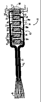
Referring now to Figure 1B, a preferred embodiment of a low profile
sensor array 10 according to the present invention is illustrated. The sensor
array
10 is configured to inhibit the sensor elements' 20 response to compression
energy
to provide a selective output which represents substantially only the acoustic
energy of interest (shear waves having short wavelengths in the acoustic
frequency
band of interest). Preferably, the sensor elements 20 include two electrically
active
layers, each of which lies on opposite sides of a neutral layer, such that the
voltage
output of the two layers produces a signal output responsive to the flexure or
-15-
CA 02361833 2001-08-31
WO 00/54897 PCT/US00/05124
change in the change in curvature of the underlying surface. As such, the
sensor
array 10 is configured to act as a mechanical filter to filter the sensor's
response to
compression energy.
Generally described, the sensor array 10 includes a frame 15 and a plurality
of sensor elements 20. The sensor array 10 is configured with a center core
layer
75 and opposing (PVDF) outer layers 50, 60 which include piezoelectric layers
500
and 600. As shown in Figure 9, each of the (PVDF) outer layers 50, 60 provides
a
pair of spatially separated electrodes 501, 502, and 601, 602 which define
first and
second signal voltages 51, 61 with respect to ground 675. As is also shown in
Figure 9, each of the outer layers 50, 60 have an external surface 50a, 60b
which
is electrically tied to the same electrical ground 675. The two opposing outer
layer
electrode surfaces 501, 502 and 601, 602 are configured to provide separate
electrical signal paths (i.e., voltage outputs V,, V2, respectively) when the
sensor
is flexed as will be discussed further below. The signal surfaces 50b, 60a are
15 preferably provided by positioning signal traces 22 (Figure 7) on the
appropriate
surface of the PVDF layer 50, 60. That is, as shown, the inner facing surfaces
of
the PVDF layers 50b, 60a, include electrical traces formed thereon.
The outer ground plane or surfaces 675 are preferably provided by applying
a conductive layer onto the outer faces of the PVDF layers 50a, 60b. For
20 depositing or forming the electrical traces 22, 22' or the ground surface,
any metal
depositing or layering technique can be employed such as electron beam
evaporation, thermal evaporation, painting, spraying, dipping, or sputtering a
conductive material or metallic paint and the like or material over the
selected
surfaces of the PVDF layers 50, 60. The ground plane is preferably formed by
applying a continuous metallized surface over the entire outer surfaces of the
PVDF layers 50a, 60b to form a continuous shield. Of course, alternative
metallic
surfaces or techniques can also be employed such as by attaching a conductive
mylar shield layer over the outer surface of the PVDF layers 50, 60.
Preferably,
conductive paint or ink (such as silver or gold) is applied to the PVDF layers
as a
thin planar layer such that it does not extend above or around the perimeter
edge
portions of the signal paths of the internal traces 22, 22'.
-16-
CA 02361833 2001-08-31
WO 00/54897 PCT/US00/05124
As shown in Figure 1B, the sensor array 10 includes a frame portion 15
with two longitudinally extending side rails, a first side rail 16, and a
second side
rail 17. Preferably, the frame 15 is configured such that the two side rails
16, 17
are spatially separate along a major portion of the length of the frame 15.
A plurality of sensor elements 20 are positioned intermediate the two side
rails 16 and 17 such that each sensor element 20 is attached to at least one
of the
sides 16, 17. Preferably, as shown, each sensor element 20 is attached to only
one
side, i.e., at a lateral attachment 18 positioned either at the first side 16
or the
second side 17. Further preferably, as shown in Figures 1A and 1B, adjacent
sensors are attached to different sides of the frame 15 and the lateral
attachments
18 extend substantially about the center of the sensor element 20. As shown in
Figures 1A, 1B, 2, 3 and 7, the sensor array 10 includes a first and second
signal
trace pattern 22, 22'. The trace patterns 22, 22' are the same and are
configured to
define two separate but corresponding active sensor electrical signal regions
25, 26,
27, 28, 29, 30 and 25', 26', 27', 28', 29', 30' across the upper and lower
PVDF
film layer sensor elements 20, 20'. The sensor array 10 is configured such
that
each corresponding sensor element electrical signal region 25, 25', 26, 26',
27, 27',
28, 28', 29, 29' and 30, 30' has a separate and corresponding electrical
signal path
25a, 25a', 26a, 26a', 27a, 27a', 28a, 28a', 29a, 29a', 30a, 30a' respectively,
defining corresponding but separate upper and lower signal paths 51, 61. As
such,
the electrical path for each sensor 25a-30a extends from a sensor element 20
to an
electrical termination or electrical connection pad 40. Although Figure 1A
illustrates only one PVDF signal layer, the opposing PVDF layer of the sensor
array 10 includes another (second or bottom) signal trace pattern 22'
substantially
similar to and configured to align with the top external trace 22 pattern
shown,
including corresponding primed element numbers. That is, upon assembly or
fabrication, two of the PVDF layers shown in the left side of Figure 1A are
disposed on opposing sides of a neutral core 75.
In a preferred embodiment, the electrical traces 22, 22' are applied to the
respective PVDF outer layer 50, 60 such as by applying a silk screened
conductive
ink or paint pattern. The ground plane is preferably provided on each PVDF
layer
-17-
CA 02361833 2007-06-13
50, 60 by applying a continuous layer of conductive ink or paint thereon. The
core
75 typically includes a neoprene layer with a thin film of adhesive on each
side.
The PVDF layers 50, 60 are then secured to the core 75 to sandwich the core
therebetween. The electrical connections (pin terminations) are made in an
external
connector and the upper and lower PVDF ground traces or surfaces 50a, 60b are
connected to a common ground 675 thereat. See U.S. Patent No. 5,595,188.
As shown in Figure 5, the sensor array 10' includes a frame 15' which can
be configured to provide supplemental structural attachments 21 at selected
areas
(such as at the ends) to further structurally tie the two sides 16', 17'
together to
help provide structural strength or positional integrity for the sensor
elements on
the array 10'. This can be beneficial for sensor arrays 10' which, once
sterilized,
are enclosed in a sterile underlying adhesive layer and sterile package for
shipment
and storage, as the sensor array is typically quickly peeled from its
packaging
during use. The additional mechanical reinforcement can minimize sensor
element
20 displacement from the frame 15'.
Figure 5A illustrates another preferred embodiment of a sensor array 10"
according to the present invention. As shown, the frame 15" includes a single
longitudinally extending side or rail 17" which is preferably widened relative
to
the dual rail configuration shown in Figure 1B to provide adequate physical
separation (to minimize the potential for electrical coupling) of the
electrical traces
22b. Of course, the electrical traces 22b will be altered to extend along the
single
rail 17".
Figures 2 and 3 illustrate a section view of a preferred embodiment of the
low profile sensor array 10. As shown (in sectional view), the sensor array 10
is
configured such that the two piezoelectrically active (PVDF) outer layers 50,
60 of
the sensor array 10 (including the outer layers of both the frame sides 16, 17
and
sensor elements 20) comprise a first material having an associated first
thickness
while a core or intermediate layer 75 comprises a second resilient material
having a
second thickness. Figure 9 schematically illustrates the electrical
configuration of
the sensor element 20 and will be discussed further below. The external traces
22,
-18-
CA 02361833 2001-08-31
WO 00/54897 PCTIUSOO/05124
22' are positioned on the respective top and bottom surfaces 50b, 60a (i.e.,
the
interior surfaces on a completed array assembly) of the outer layers 50, 60.
As shown, the core 75 thickness is greater than the thickness of the outer
layers 50, 60. In a preferred embodiment, the core 75 is an order of magnitude
thicker than the outer layer thickness. More preferably, the core 75 has a
depth or
thickness of about 600 microns while the outer layers 50, 60 are about 30
microns
thick. It is also preferred that the core material be selected such that it
has a
relative permittivity which is less (and more preferably much less such as an
order
of magnitude less) than the relative permittivity of the outer layers 50, 60.
In one
embodiment, a suitable core relative permittivity value is about 5 or 6.
It is also preferred that the core materia175 be selected such that it is
resilient or compliant (substantially incompressible material) and preferably
has
low viscous losses. "Resilient", as used herein, means that the core is sized
and
formed of a material which allows the sensor array (at least the sensor
element) to
be conformal to the underlying surface when in position. Stated differently,
the
core 75 is configured such that at least the sensor elements 20 are
substantially
compliance matched with the body, i.e., to follow the shape of the underlying
patient skin surface when positioned thereon. Preferred core materials include
nitrile, neoprene, latex, polyethylene, or high-density polyethylene forms. In
a
preferred embodiment, the core material is neoprene. Alternatively, the core
75
can be formed as a thin layer of insulator (a neutral center), allowing the
two
opposing electrically active layers 50, 60 to be electrically separated and
directly
responsive to the flexure of the underlying surface.
In a preferred embodiment, the core 75 has a first relative permittivity and
the outer layers 50, 60 are first and second pliable material layers which
have a
second relative permittivity. The first relative permittivity is less than the
second
relative permittivity. As such, the resulting capacitance of the core 75 may
be such
that it is about an order of magnitude less than the PVDF layers 50, 60. In a
preferred embodiment, the core 75 is sized to have a greater thickness than
the
PVDF layers 50, 60. The core 75 capacitance is related to the material and
configuration of the core 75. More particularly, the core 75 capacitance is
related
-19-
CA 02361833 2007-06-13
to the core material permittivity (s), and the core configuration (area (A),
and the
thickness (1)) as stated by the equation (C= EA/1). In a preferred embodiment,
the
sensor 20 is configured such that the capacitance of the core 75 is less than
that of
the electrodes defined by the PVDF layers 50, 60.
Referring to Figures 2, 3 and 9, the outer layers 50, 60 are formed from a
piezoelectrically active material such as, but not limited to, polyvinylidene
fluoride
(PVDF) or its copolymer with trifluoroethylene (PVDF-TrFe). As shown in
Figure 9, electrodes 501, 502, 601, 602 are formed on both sides of the major
surfaces of piezoelectric film 500, 600. In this way, the PVDF material
provide
outer layers 50, 60 which function as electrodes which can act as an
electromechanical transducer and, as such, can be used as an acoustic sensor
20.
Generally described, and as shown in Figures 14A, 14B, and 14C, the sensor 20
is
configured such that when the piezoelectric material is subjected to strain or
stress
(flexure or curvature displacement) an electric potential or voltage
proportional to
the magnitude of the strain or compression is developed across the thickness
of the
piezoelectric material. See e.g., U.S. Patent No. 5,885,222. A preferred
electrical
configuration will be discussed further below.
Figure 4 is a side view of a low profile sensor array 10 according to a
preferred embodiment of the present invention. As shown, the sensor array 10
is
configured such that each of the sensor elements 25-30 and the frame 15 are in
(substantially) coplanar alignment along at least the top surface 10a of a
major
portion of the frame 15 region when viewed from the side (i.e., the sensors 20
and
sides 16, 17 have the same material thickness and layers). More preferably, as
shown, the sensor array 10 (and the sensor array 10" with the single rail
frame
15") is configured such that the elements 20 and the frame 15 have the same
profile configuration along the top and bottom surfaces 10a, lOb. The sensor
array
10 is substantially flush across the top and bottom surfaces 10a, lOb. As
shown,
the linear strip array preferably includes a top and bottom outer surface 10a,
l Ob
with a substantially constant and flat profile. Alternatively, as will be
discussed
further below, the top outer surface can include one or more discrete masses
900 or
-20-
CA 02361833 2001-08-31
WO 00/54897 PCT/US00/05124
stiffeners 910 attached to the sensor element region to modify the response of
the
flexural sensor element 20 (Figure 26).
Figure 5 shows an alternate embodiment of a sensor array 10'. In this
embodiment, the lateral attachments 18' extend about alternating forward and
rearward edges of the sensor elements 20. Also as shown, the sides or side
rails
16', 17' have a greater lateral length, providing additional area for the
signal traces
22. The additional area can allow the separate paths to be spatially separated
by a
greater separation distance or can allow additional sensor elements 20 to be
used
(more area used for additional traces needed for the additional elements). The
additional width of the sides 16', 17' can also help minimize electrical cross
talk
along the length of the signal path. Similarly, Figure 5A illustrates a single-
rail
embodiment of a sensor array 10" according to the present invention. As shown,
the sensor arrays 10, 10', 10" include a plurality of sensor elements 20
(preferably
more than four sensor elements, and more preferably six or more sensor
elements).
Turning now to Figure 6, a preferred structural foundation layer 100 is
shown. The foundation layer 100 provides the structural foundation for the
signal
traces 22, 22' which are preferably applied to the PVDF layers 50, 60 and
attached
to the foundation layer 100, as will be discussed further below. As shown, the
foundation layer 100 defines the frame 15, the side rails 16, 17 and the pads
for the
sensor elements 20. It also includes a neck portion 102 which separates the
frame
upper portion which includes a resilient core material to a thinner ribbon
portion
105 (which extends down to the terminal connection ends at the connector (not
shown)). In any event, the neck portion 102 of the frame 15 is preferably
configured to transition the sensor array from one thickness to another such
that the
core 75 has a first thickness at the neck upper portion 102 but substantially
terminates prior to the end of the neck lower portion 105 to a second reduced
thickness. Preferably, a shown in Figure 6, the sensor array 10 is configured
such
that the neoprene extends down until the area shown in cross hatch. A
preferred
neoprene stop zone 76 is shown at position A- A. Preferably, the ribbon 105 is
configured such that the PVDF electrically active surfaces do not contact. For
example, other thin insulating core materials such as a double sided
polyethylene
-21-
CA 02361833 2001-08-31
WO 00/54897 PCT/US00/05124
film can be positioned such that it extends between the two inwardly facing
surfaces of the PVDF layers 50, 60.
Figure 7 illustrates a preferred trace pattern 22, 22' which is, upon
assembly, positioned onto the appropriate surfaces of the film layers 50, 60
forming the respective electrical regions for the sensor elements 25-30, 25'-
30' and
respective signal paths 25a-30a, 25a'-30a' which extend down the neck portion
102 and ribbon portion 105 of the sensor frame. As shown in Figure 7, the
electrical pattern 22, 22' includes a sensor pad active region 220 and linear
traces
221. The trace pattern is disposed onto the piezoelectric layers 50, 60 as
described
above. Preferably, it is formed by applying conductive ink, such as disposing
onto
the outer surfaces of the outer layers 50, 60 a silver ink silk screen
pattern. While
particular conductive patterns are illustrated in Figures 7 and 5A,
alternative
conductive patterns may also be used. For example, conducting paint, flex
circuits,
foil or other coating or metal deposition methods and techniques may also be
employed. It is preferred that, if flex circuits are used, that they are
configured or
attached to the foundation layer 100 so as to be transparent to the structure
of the
sensor array to minimize any potential interference with conformance of the
sensor
element to the body.
For clarity, it will be understood that, according to the present invention,
protective films or coatings may also be positioned over the PVDF "outer"
layers
forming the ground and signal planes (or traces) as long as they are applied
so as to
be substantially transparent to the operation of the sensor elements.
Therefore, as
used herein, the trace(s) 22, 22' or outer layers 50, 60 can include traces or
layers
which are covered with moisture barrier coatings, adhesives, or other
materials and
are thus not truly "external" or "outer" as described for ease of discussion
herein.
Figure 8B is an enlarged view of a sensor element 20. Preferably, the
sensor element 20 is substantially rectangular with side dimensions of from
about 8
mm to about 11 mm. In a preferred embodiment, as shown in Figure 9, the upper
and lower traces 22, 22' are deposited onto the inwardly facing major surfaces
of
the (PVDF) layers 50, 60. As such, the electrically active regions defining
the
signal paths include the pad regions 25, 25' and the signal lead paths 25a,
25a'
-22-
CA 02361833 2007-06-13
which are spatially separated a distance from top to bottom about a central
neutral
core 75. The PVDF outer layers 50, 60 are preferably relatively thin (such as
below about 60 microns, and preferably about 30 microns) while the core depth
75a
is an order of magnitude greater (above 300 microns, and more preferably above
about 500 or 600 microns). This configuration makes the thickness of the PVDF
layer 50, 60 relatively structurally negligible compared to the depth or
thickness of
the core 75. As shown in Figure 9, the upper and lower signal paths 502a, 602a
defined by the trace patterns 22, 22' are separated by a distance which is
substantially equal to the core depth 75a.
Figure 10 schematically illustrates a preferred configuration of a low
profile sensor array assembly 120. As shown in Figure 10, the sensor array
assembly 120 includes four laterally positioned linear sensor or strip arrays
120a,
120b, 120c, 120d in electrical communication with a signal processor 150
(having
an opto-isolator 151). Figure 10 illustrates four sensor arrays 10 positioned
over
preferred intercostal spaces. See pending PCT/US99/26198 and U.S. Patent
Numbers 6,193,668 and 6,371,924. Figure 10 also illustrates a preferred
pigtail
arrangement for the sensor array assembly 120. As shown, the pigtail 120P
preferably extends off the sensor elements toward the sternum of the patient,
thereby allowing standard cord sizing notwithstanding the access to the
patient
(i.e., whether the system must be hooked to the patient from the right or left
hand
side of the bed). Alternatively, as shown in Figure 11, the electrical
pigtails 120P
can extend from the opposing side.
Similarly, Figures 11 and 12 illustrate a preferred low profile sensor array
120 assembly positioned on a subject which comprises four linear array sensors
10,
the sensors having six sensor elements 20 each. Of course, alternative numbers
of
sensor arrays 10 or sensor elements 20 on the arrays 10 can also be used
(either in
combination or alone). Figure 12 illustrates the low profile acoustic sensor
array
10 positioned on the skin 200 of a patient over an acoustic window above the
cardiac region of interest. Thus, the sensor array according to the present
invention
preferably includes means for releasably securing the sensor array to a
patient.
- 23 -
CA 02361833 2001-08-31
WO 00/54897 PCT/US00/05124
Such means may comprise an adhesive layer which may be incorporated in or
applied to one side of the sensor array such as the adhesive layer 775 shown
in
Figure 9. Suitable adhesives for releasably securing medical apparatus or
devices
to a patient are known to those of skill in the art. As shown in Figure 9, the
sensor
array 10 also preferably includes a release adhesive 775 positioned along a
major
portion of the lower external surface 60b to secure the sensor array to a
patient
during clinical use. Of course, sterile adhesive creams, double-sided tapes,
and the
like can alternatively or additionally be used to position the array on the
patient's
skin.
Turning now to Figures 9, 13A, 13B, and 14A-C, preferred electrical and
operational schematics for the sensor elements 20 are shown. As discussed
above,
Figure 9 illustrates the piezoelectric active outer layers 50, 60 as including
a
PVDF (or other piezoelectric polymer) portion 500, 600 and two corresponding
opposing first and second interior active electrode surfaces. or layers 501,
502 and
601, 602. The interior film surfaces 502, 602 each include a separate
electrical
signal path 502a, 602a while the outer film surfaces 501, 601 are tied to a
common
ground 675.
Figures 9 and 13A-B illustrate that the PVDF is disposed on the first
(upper) outer layer 50 with a polarity of negative to positive. That is, the
major
inner surface 50b has a positive polarity while the major outer surface 50a
has a
negative polarity. In contrast, the PVDF is disposed on the (lower) outer
layer 60
with the reverse polarity; positive on the major inner surface 60a, and
negative on
the major outer surface 60b. Of course, the layer polarities could also be
reversed
(i.e., the upper layer 50 can have negative to positive while the bottom layer
60 can
have positive to negative).
As shown in Figures 14B and 14C, each of the outer layers 50, 60 provides
a voltage (V, and V2) 51, 61 in response to flexure of the sensor 20,
respectively,
even in response to long compressional waves. However, in response to gross
translation of the sensor 20 which does not result in flexure, no voltage will
result.
Because the polarities are reversed, and because the core material and sensor
configuration provides a high degree of coupling between the two outer 50, 60
-24-
CA 02361833 2001-08-31
WO 00/54897 PCT/US00/05124
active (electrical) layers, the absolute value of the voltages for a
particular flex or
curvature will be substantially the same. However, because during flexure or
curvature of the sensor, one layer is in compression and the other layer in
tension,
the sign of the voltage will be opposite between the two layers. Further, if
movement of the sensor does not result in curvature of the sensor, then the
polarity
of the sign will be the same between the two layers. Thus, the instant sensor
configuration is preferably configured to read the voltage differential of the
two
voltages, that is the difference between the response voltages V,, VZ..
Advantageously, as shown in Figure 13a, the electrode configuration is
such that the sensor 20 acts like a differential amplifier 63. In operation,
the sensor
array 10 takes the voltage differential of the two response voltages V,, V2 to
generate a signal response which has an increased voltage value (approximately
doubled value) and, thus, can provide improved SNR performance. Further, for
non-flexure sensor excitation, the voltage polarities are such that the signal
responses from each layer 50, 60 cancel each other, minimizing signal output
for
non-flexure excitations.
Thus, in operation, as schematically shown in Figure 14a, for a non-strain
input such as a compression wave (typically input to the sensors by ambient
noise
that is carried by noise in the air, or noise that is transmitted through
structural
vibration), both the top and bottom sensor layers see the same force, and
without a
strain or flexure to cause a curvature in the layers 50, 60 the polarity of
the voltages
are such that any signal response"is cancelled and no signal output is
transmitted
for detection. In contrast, as shown in Figure 14b and 14c, the polarities of
the
layers 50, 60 associated with the strain in the PVDF or outer (electrical
response)
layers 50, 60 have opposing polarities. For example, for a given flexure in
the
outer layer 50, and a(V,) response of 2 microvolts, the (V2 ) response may be
about
(-2 microvolts), and the signal response for this flexure will then be 2-(-2)
or 4
microvolts. Of course, the magnitude of the voltage will vary according to the
degree of strain or curvature of the flexure.
Figure 14a illustrates the substantial non-response associated with a
compression or longer wavelength transmitted across the sensor situs while
-25-
CA 02361833 2001-08-31
WO 00/54897 PCTIUSOO/05124
Figures 14b and 14c show the voltage response (opposing polarity)
corresponding
to flexure at shorter wavelengths of interest. As shown, the voltage polarity
corresponding to an upward flexure is positive for the upper PVDF layer 50 and
negative for the lower PVDF layer 60 and the polarities reverse for a downward
flexure.
In a preferred emb6diment, as schematically shown in Figure 14d, the
sensor arrays 10,10',10",10"'are configured such that they are selectively
responsive to shorter wavelengths 310 that cause flexure through the thickness
of
the sensor element 20, 420, while being substantially non-responsive or
resistant to
longer acoustic wavelengths 300. The longer wavelengths 300 are typically
associated with compression waves in the body or in the ambient noise within
the
examining room, and which cause compression through the thickness of the
sensor
element. In operation, due to differences in the speed of the waves or a
frequency
band of interest, shear waves typically have much shorter wavelengths than the
wavelengths associated with compression waves. Stated differently, the sensor
is
responsive to the flexural mode of displacement caused by short wavelengths of
shear waves 310, and substantially non-responsive to acoustic inputs of the
much
longer compression wavelengths 300. At the same time, the sensor array is
configured to respond to shear waves having shorter wavelengths 310. Thus, the
sensor array 10 of the present invention acts as a mechanical filter and
inhibits or
minimizes the sensor elements from generating a detectable signal response for
long wavelengths at frequencies of interest. The sensors and sensor arrays
described herein include an operational range for the acoustic wavelengths of
interest for the diagnosis and detection of coronary artery disease.
Preferably, the
sensors include an operational range of at least about 100-2500 Hz, and more
preferably a range of about 100-1000 Hz. Preferably, the sensor elements 20
are
configured and sized on the frame 17 to respond to shear waves at the
operating
frequencies of interest such as those characterized as having propagation
velocities
of less than about 25 m/s, or more in the range of about 5-15 m/s, and to
suppress
or inhibit signal response for compressional waves or acoustic waves having a
propagation velocity above about 100m/s. More preferably, the sensor is
-26-
CA 02361833 2001-08-31
WO 00/54897 PCTIUSOO/05124
configured to suppress response associated with the wave speed of
compressional
waves in the air, typically a velocity of about 340 m/s and the response
associated
with the wave speed of compressional waves in the body, the compressional wave
velocities being typically about 1540 m/s in the body.
Figure 8A illustrates an alternative discrete or single sensor embodiment of
the present invention. The signal return covering the back of the film has
been
removed for clarity. It is preferred that the width of the pigtail be
configured and
sized to hold the capacitance of a signal trace below about 10% of that of a
sensor
element. As shown, the single sensor 201 includes a positive signal 280 and
negative signal 281 electrical path which is formed by the two PVDF layers
50j,
60j similar to the electrical traces 322,322' formed onto the outer PVDF
layers of
the strip array 10 discussed above. As shown, the single element 201 can be
formed by configuring four signal lines on a single sheet of PVDF material.
The
single sheet is configured to be folded, such as along the dotted fold lines
shown,
to provide the two interior signal paths 280, 281 and the external common
ground.
The two grounds 290a, 290b are preferably formed by a metallized mylar shield
290 configured to provide a continuous planar electrical shield on one surface
of
the PVDF material (the surface opposing the electrical traces 322, 322'). The
electrical pin out can also be alternatively configured as will be appreciated
by one
of skill in the art.
Figures 17A and 17B illustrate yet another preferred embodiment of an
accordion pleated sensor array 10"' which can advantageously minimize
mechanical vibration and cross-talk between sensor elements 421, 422, 423 and
their associated transmission lines 431, 432, 433 while also providing a
mechanical
filter (to reject compression energy and allow selective acoustic response as
discussed above) according to the present invention. This low profile acoustic
accordion array is also configured to selectively respond to shear waves while
rejecting compression wave energy in the frequency range of interest. As
shown,
this sensor array 10'11 includes multiple discrete or unitized sensors 420 and
corresponding individual transmission lines 430 which are electrically
connected at
a primary connector 450 and into the signal processor operating system 1501.
As
-27-
CA 02361833 2001-08-31
WO 00/54897 - PCTIUSOO/05124
shown in Figure 17B, the sensor array 10"' preferably includes three sensor
elements 421, 422, 423 with corresponding transmission lines 431, 432, 433.
The
separate transmission lines 431, 432, 433 can substantially isolate each
element
and respective transmission line to thereby minimize the cross talk between
adjacent sensor elements.
As is also shown in Figure 17B, the transmission lines 431, 432, 433 are
preferably folded or formed with a series of undulations 435 along the length
of the
transmission path (the transmission path extending between the sensor element
420
to the primary connector 450). Although shown as formed with accordion type
"sharp" creased or crimped edges ("pleats"), it will be appreciated by one of
skill
in the art that other mechanical damping configurations may also be used. For
example, but not limited to, the transmission line can be formed with a series
of
sinusoidal curves or waves or folds formed along a portion of its length, or
formed
with alternating material widths (e.g., thin to wide, wide to thin), or a
combination
of fold or curve patterns, interposed extra material or alternating material
composition, weight, and the like. As used herein, the term "undulating"
includes
the above mechanical damping configurations.
Figures 17A and 17B illustrate a preferred sensor array 10"' alignment.
As shown, in position on a subject, the sensor array 10"' positions the sensor
pads
421, 422, 423 such that the discrete sensor pads are configured as an array
10"'
with a plurality of unitized, separated, or discrete sensors; that is, the
sensors 421,
422, 423 and corresponding transmission lines 431, 432, 433 are configured as
discrete aligned segments in the array, i.e., they have "unitized separation".
As
shown, the rear of the sensor pad 423b of the most distal sensor 423 (the
sensor
positioned closest to the center of the subject's chest) is proximate to the
front
422a of the next adjacent sensor pad 422. The rear of that sensor pad 422b is
positioned proximate to the front 421a of the next sensor pad 421. Further
preferably, as shown, the sensor pads 421, 422, 423 are positioned such that
they
are substantially linear arranged and symmetrically extend relative to a
horizontal
or lateral alignment axis A-A. Further, it is preferred that each of the
sensor pads
is conformal to the underlying skin and the transmission lines are sized and
-28-
CA 02361833 2008-03-20
configured such each is spatially separated from the others (i.e., non-
contacting
with the others).
The transmission line 430 preferably longitudinally extends off one end
portion of the sensor pad (shown as the rear portion) 423b, 422b, 421b.
Preferably,
the sensor array 10"' is configured and sized such that the transmission line
for
each sensor 430 extends off the sensor pad in a manner that, when connected to
the
system connector 450 and securely attached to the surface of the patient, the
transmission line 430 defines a concave contour along a portion of its length
when
viewed from the side. That is, as shown by Figures 17A and 17B, the length of
the transmission line 430 is such that it is sufficiently long when in
position so as
to provide a suitable amount of slack to prevent tensioning of the
transmission line
when the primary connector 450 is connected to the signal processing input
port
1501. In addition, as shown, the sensor array 10"' is configured such that the
array
includes three discrete sensors 420, and each sensor 420, sensor pad 421 423,
and
associated transmission line 430 is a substantial mirror image of the other
sensors,
sensor pads, and transmission lines. However, the sensor array 10"' can
include
alternative numbers of sensors such as 2, 4, 5 or more. In addition, the
system can
employ several of the multi-element sensor arrays 10"' (such as four) of the
tri-
sensor discrete element sensor array 10"' (not shown). This plurality of three
element sensor arrays 10"' can reduce the number of patient interconnections
undertaken by a technician at patient application in order to prepare the
equipment
for use, while still allowing twelve individual sensor pad elements to be used
for
more precise acoustic detection on a patient.
Figure 17A also illustrates a reflector 424 positioned on each of the sensor
elements 420 to facilitate the detection system's photogrammetric recognition
of the
positional alignment of the sensor elements 420 when on the body. The
reflector
424 can be applied by various means such as via reflective paint or by
attaching
reflective tape to the external (exposed) surface of the sensor element 420.
See
e.g., co-pending and co-assigned U.S. Patent Application Publication
No. 2001-0034481, to Van Horn, entitled "Methods, Systems, and Computer
-29-
CA 02361833 2007-06-13
Program Products for Photogrammetric Sensor Position Estimation."
Referring now to Figure 18A, the sensor array 10"' is shown in a pre-use
position (not positioned on a subject). Each sensor 420 includes a sensor pad
420p
and a termination end 440. The termination end of the sensor 440 is connected
to
the primary connector 450. In a preferred embodiment, a mechanical termination
stiffener 441 is applied over the termination ends 440 adjacent the primary
connector 450 to help stiffen and support the relatively thin ends of the
sensors
420. Preferably, the termination stiffener is formed of a non-conducting
material
such as a transparent film or the like. Suitable materials include polyester
and/or
polystyrene and the like. Also preferably, each sensor 420 has a discrete or
unitized termination stiffener 441 which is spatially and mechanically
separate
from the others to help isolate each of the signal paths from the others. The
termination stiffener helps provide sufficient structure for the relatively
thin
flexible PVDF body 420b (Figure 20A) onto which the connector or end
terminations can be attached. Of course, alternate structural enhancing means
can
also be used as will be appreciated by those of skill in the art.
As shown in Figures 18A and 18B, the transmission lines 430 each include
a plurality of undulations or pleats 435 formed along the length thereof
(typically
under about 23 cm). Preferably, each transmission line 430 is configured the
same
as the others. In a preferred embodiment, as shown, each transmission line 430
preferably includes at least four undulations or pleats 435 serially formed in
continuous repeating (non-interrupted) fashion along a major portion of the
length
thereof. Of course, as will be appreciated by one of skill in the art, the
number of
pleats, the shape, and the pattern or configuration of same can be
alternatively
arranged. The undulations or pleats 435 positioned along the transmission
lines
430 help to isolate the transmission paths so as to minimize the sensor
array's 10"'
reaction to unwanted acoustic inputs between adjacent elements or lines or
even
from vibration from a computer or processor or data system connected to the
array
for receiving the data signals associated with the flexure responsive
generated
signals. In another preferred embodiment, the pleats 435 or undulations begin
-30-
CA 02361833 2001-08-31
WO 00/54897 PCTIUSOO/05124
substantially immediately after the sensor pad 420p and extend continuously
about
every 0.5 inches or 1.25 cm (0.5 inches or 1.25 cm edge to edge) along the
length
of the transmission line 430 until the termination end of the sensor 440.
It is also preferred that the electrical lead lengths of the transmission
lines
430 and each of the sensor pads 420p are maintained as a constant size and
length
to allow for the differential sensing capability such as discussed under the
section
describing the other sensor array configuration above.
Referring now to Figures 19A and 20A, a preferred embodiment of a
sensor body 420b is shown. Similar to the embodiment shown in Figure 8A, the
sensor body 420b includes a thin layer of piezoelectric film 420f ("PVDF")
having
opposing first and second major surfaces 420fa, 420fb. The first major surface
420fa of the film includes an active metallized electrode surface 22e defining
the
opposing sensor pad regions 420p1, 420p2. The first major surface 420fa also
includes the separate electrical traces 480, 481. Preferably, the electrical
traces
outside the electrode regions are inactive, for example, by the trace regions
not
being initially polarized, or depolarized such that they act to carry or
transmit
flexure signal generated by the electrode sensing regions.
The second major surface 420fb of the PVDF film layer 420f (the surface
underlying the exposed surface shown in Figure 19A) is formed from a
conductive
trace such as a conductive ink (but of course other methods for disposing a
conductive trace can also be used such as those described hereinabove). As
shown
in Figure 19B, the second major surface 420fb is preferably configured to
provide
a continuous conductive active surface pattern 22e' which includes the upper
portion of the "T" defined by the two pad portions of the sensor body 420p1,
420p2. The second major surface 420fb also includes a trace 438g positioned
along one side of the (PVDF film). This third transmission line or trace 438g
acts
as a ground signal path or line.
In a preferred embodiment as shown in Figure 19B, the trace 438g is
preferably configured to extend a greater distance on the termination end of
the
sensor 440 and thus form the long finger portion 440f of the termination end
of the
sensor. This additional length allows this portion of the sensor to be folded
over to
-31-
CA 02361833 2001-08-31
WO 00/54897 PCTIUSOO/05124
the other side of the sensor to align the ground signal line 438g with the
signal
transmission lines 438b, 438c for each of the electrodes 450, 460. As shown in
Figures 21B and 22, this termination configuration provides a four point
termination, one each associated with the electric shield "ground" 438a, the
PVDF
film layer traces 438b, 438c, and the folded 438g ground trace. The four-point
termination connection for the primary connector 450 is thus configured on a
single common connection surface.
The PVDF film layer 420f defines the acoustic sensor signal paths 480,
481, and ground signal path 438g for, each of the sensor pads or electrodes
450,
460, including the active portion of the sensor pad 420pl, 420p2 and the
associated transmission or signal paths 438b, 438c, 438g. Similar to the
operation
of the differential sensor 63 explained for Figure 13 and 13A, the PVDF film
420f
is preferably configured to provide opposing sensor pads 420p1, 420p2 which
act
as electrodes 450, 460 having opposing polarities. As shown in Figure 20B, the
negative and positive polarity associated with the upper and lower electrodes
450,
460 provide the differential configuration for the flexure induced voltages
v,, vZ.
Of course, as note for the above-described embodiment, the polarities can also
be
reversed, but the sensor region is preferably configured with opposing
polarities for
the sensor pad in order to provide the differential based operational sensing
configuration. In any event, as shown, the PVDF film layer 420f is configured
to
provide an upper electrode surface and a lower electrode surface 450, 460,
respectively (the lower electrode surface and the surface shown in Figure 19A
disposed on the patient such that these surfaces face the skin of the
patient).
Preferably, as shown in Figure 20A, in order to form the sensor assembly
420, a layer of nonconductive material (such as polyester film) 499 is
attached to or
applied to overlie substantially the entire length of both sides of the PVDF
film
layer 420f along the linear transmission line 430 or trace portion of the
sensor body
420b (excluding both sides of the sensor pads 420p1, 420p2 or upper portion of
the "T" region of the sensor body). Preferably, as is also shown, the
polyester film
layers 499 end a distance away from the termination end of the sensor 440 --
substantially along a line shown by P-P in Figure 19A and Figure 21B. A single
-32-
CA 02361833 2001-08-31
WO 00/54897 PCTIUSOO/05124
sided or double sided adhesive-backed polyester tape can be conveniently used
to
attach the polyester layers to the respective PVDF film surface 420fa, 420fb.
Of
course, other adhesive or attachment means can also be used as will be
appreciated
by one of skill in the art.
The sensor body 420b also includes a resilient core 75' which is applied to
one side of the sensor pad region of the sensor body 420b as shown by the
arrow
associated with the core element 75' drawn in dotted line in Figure 19A.
Figure
20A also shows the preferred assembly position of the core 75' relative to the
sensor pad 420p2 region of the sensor body 420b. In position, the core 75' is
positioned to overlie and attach to the sensor pad 420p2 (such as via an
adhesive).
As shown in Figure 20A in double-dotted line, to form the flexure-responsive
sensor element 421-423, the PVDF film sensor pad 420p1 is folded over the
central core layer 75' to overlie the opposing PVDF film sensor pad 420p2 as
shown in cross section in Figure 20B. The folded configuration of the sensor
420
(that is preferably only the sensor pad region is folded) is shown in Figures
18A
and 18B.
As is also shown in Figure 20A, in this embodiment, first and second
layers of conductive shielding material layers 501, 502 are attached to the
sensor
body 420b. In a preferred embodiment, the shielding material layers are
metallized
film, and more preferably a thin sheet of MYLAR film. The conductive
shielding material layers 501, 502 help to shield the sensor 420 to minimize
the
introduction of electromagnetic interference into the sensor signal paths. As
shown
in Figure 20A, the shielding material layers 501, 502 are sized and configured
so
that they do not contact along the sensor pad region of the sensor, i.e., the
perimeter edges of the sensor pad are not enclosed by the shielding material
layers
501, 502 when the PVDF film sensor pads are aligned over the core 75'.
As shown in Figure 20A, the first shielding layer 501 linearly extends from
the upper neck portion of the sensor body to an end portion which is adjacent
the
termination end of the sensor 440. In this embodiment, the first shielding
layer
does not extend to cover the PVDF sensor pad regions 420p1, 420p2. As is also
shown, the first shielding layer 501 ends at substantially the same position
as the
-33-
CA 02361833 2001-08-31
WO 00/54897 - PCT/US00/05124
polyester layer 499 but also includes a termination protrusion end 438a which
longitudinally extends a further distance to align with the active signal
transmission lines 438b, 438c.
Figure 21A shows the preferred end point for the non-conducting layers
499 and the upper shielding layer 501. As shown, the material extends adjacent
but below the sensor pad regions 420pl, 420p2. Figure 21B shows the outer
shielding material layer 501 positioned on the PVDF film layer 420f. As noted,
the shielding layer 501 and the intermediately positioned polyester layer 499
end at
a common termination line P-P for a major portion of the outer shielding
material
layer 501. This configuration allows electrical access for the signal lines
438b,
438c. This configuration also allows for electrical engagement with the ground
path 438g when it is folded up to contact the shielding material layer 501.
As shown in Figure 20A, the second or opposing outer shielding layer 502
is configured and sized to substantially conform to the shape and size of the
unfolded PVDF film layer 420f. As such, it includes a "T" shaped body of which
the upper portion is preferably folded along with the sensor pad 420p1. When
folded, the second shielding layer 502 provides a continuous electric shield
for the
exposed major surfaces of the sensor pad 420p and also preferably ends into or
contacts the upper portion of the first shielding layer 501a at a lower edge
502a.
Accordingly, the two opposing shielding layers 501, 502 provide a contiguous
shield for the sensor 420 as shown in Figure 17A while the insulating
polyester
film layer maintains the electrical integrity of the internally disposed
signal paths
438b, 438c. Similar to the first shielding layer 501, the second shielding
layer 502
also includes a longitudinally extending protrusion portion 438a' positioned
to
overlie the first protrusion 438a with the PVDF film layer 420f disposed
therebetween. Upon termination into the connector, the protrusion portions
438a,
438a' provide the electrical continuity for the shield layers 501, 502.
Figure 22 illustrates the electrical signal paths 438a, 438b, 438c, and 438g
formed onto the sensor body 420b. The live signal paths with opposing polarity
are 438b and 438c, while the ground is provided by 438g and the shield by
438a,
438a'.
-34-
CA 02361833 2001-08-31
WO 00/54897 PCT/US00/05124
Advantageously, as shown in Figure 20b, the electrode configuration 450,
460 is such that the sensor 420 acts like a differential amplifier 63' as
discussed for
the embodiment described above. In operation, the sensor 420 takes the voltage
differential of the two response voltages v,, v2 to generate a signal response
which
has an increased voltage value (approximately doubled value) and, thus, can
provide improved SNR performance. Further, for non-flexure sensor excitation,
the voltage polarities are such that the signal responses from each layer 450,
460
cancel each other, minimizing signal output for non-flexure excitations.
Preferably, the sensor component materials such as for the core are selected
and configured as described for the first embodiment described herein.
As shown in Figure 23, the sensor array 10"' preferably includes a
structural support or carrier member 600 which is positioned over the exposed
side
of the plurality of sensors 420 (the side away from the patient when in
operable
position). The carrier member 600 is release-ably secured to each of the
plurality
of sensors 421, 422, 423. Thus, the carrier member 600 is used to maintain the
sensor elements 421, 422, 423 in a predetermined alignment so that an operator
or
technician can remove the sensor array from a shipping package, attach the
discrete
sensor elements 421, 422, 423 onto the patient, and strip the carrier member
600
away, conveniently providing unitized installation for discrete sensors. The
underside of the sensor elements 421, 422, 423 preferably includes a layer of
adhesive which is configured to securely attach the sensor's in position on a
patient
during use as described for the first embodiment above (of course, the
adhesive can
be directly applied to the patient instead). The carrier member 600
conveniently
allows the technician or operator to easily position the discrete individual
sensor
elements 421, 422, 423 onto the patient while maintaining the preferred
alignment
positional relationship therebetween. Thus, the carrier member 600 is
configured
to be temporarily attached to the sensor elements 421, 422, 423 (only during
shipping and patient application, i.e., attached during the time period prior
to
sensor operation). Advantageously, the carrier member 600 can limit the number
of installation steps the operator must take to prepare the patient for
acoustic
evaluation. Further, the carrier member 600 is configured to release or detach
from
-35-
CA 02361833 2001-08-31
WO 00/54897 PCT/US00/05124
the sensors 421, 422, 423 once the sensors are secured to a patient. Of
course, this
carrier member can also be used with other flexible low profile sensor arrays
to
help facilitate the positional and structural integrity while applying same to
the
patient.
This disengagement is preferably accomplished by disengaging an edge
portion of the carrier such as an exposed tab 601 and pulling the carrier
member
600 away from the sensor elements 421, 422, 423 without disturbing the
installed
position of the sensors on the patient. Advantageously, the carrier member 600
provides the installation convenience of structurally related sensors while
also
allowing the structural isolation of the sensors during operation.
Figure 27 schematically illustrates the preferred product configuration with
the releasable carrier member 600. Step 1 includes a first carrier member 600
and
a second carrier member 619 used during transport or shipment to a use
facility
(step 1). As shown, the second carrier member is an easily releasable (low
peel
strength) tape or the like which is used to protect and maintain the patient-
adhesive
material intact during shipment. Step 1 also shows that prior to use, the
second
carrier member is pulled away and released exposing the bottom of the sensor
elements and the adhesive thereon. Step 2 illustrates that, once the sensor
elements
are secured to the patient, the top carrier member 600 can be pulled away
leaving
the sensor elements exposed. Thus, the top carrier member 600 preferably has a
peel strength which is less than the bond strength of the adhesive/patient
attachment. The top surface of the sensor elements can also include discrete
masses or reflectors as will be discussed further below. Step 3 illustrates
the
positional alignment of the sensor elements 420 provided by the fixed
structural
relationship via the top carrier member 600 during positioning onto a patient.
Thus, conveniently, once the top carrier member 600 is stripped away, the
sensor
elements 420 are in position and ready for acoustic operation. The carrier
member
600 is particularly helpful for discrete element sensor arrays 420, but the
present
invention is not limited thereto, and can of course, be employed with the
strip array
10 embodiment described herein.
-36-
CA 02361833 2001-08-31
WO 00/54897 PCT/US00/05124
Another preferred embodiment of the present invention includes a sensor
array 10"'M as shown in Figure 24A. In this embodiment, at least one discrete
mass 900 or external flex stiffener 910 is added to the upper (exposed when on
a
patient) surface of each sensor element 420. This configuration can modify the
flexural response of the sensor element 420 and may improve the coupling of
the
sensor. Preferably, the discrete mass 900 or external stiffener 910 extends
across
at least a portion of the short dimension of the sensor element. It is also
preferred
that the mass (or stiffener) be sized and configured on the sensor element 420
such
that it is locally discrete as opposed to distributed (distributed meaning
extending
continuously across the long dimension of the sensor element).
In a preferred embodiment, as shown in Figure 24A, a centrally positioned
discrete mass is positioned on each sensor element 420. Preferably, the mass
is
formed from a high-density material such as a tungsten alloy, lead, or other
heavy
metal. A suitable discrete mass 900 weighs about 3-6 grams, and more
preferably
about 4.5-5 grams. Typical dimensions of the discrete mass is about 0.2x 0.2 x
0.42 inches (or about a 5mm length across the short dimension of the sensor
pad).
Examples of discrete external stiffeners include a layer of material having a
different (more rigid) stiffness as compared to the PVDF layers or the core.
Figures 24A-E, 25A-C, and Figure 26 illustrate exemplary discrete mass
and stiffener configurations according to the present invention. Figure 24B
illustrates a plurality of discrete masses 901 positioned on opposing ends of
the
sensor elements 420. Figure 26 illustrates a discrete mass 900 positioned on
the
strip array 10. Figure 24C illustrates a discrete mass 900 positioned on the
sensor
element 420 and a discrete mass 900 and a second discrete mass 900a positioned
on the transmission path 430. Figure 24D illustrates a plurality of discrete
masses
900 positioned onto the sensor pad 420. Figure 24E shows a plurality of
alternately configured discrete elements 902 positioned on the sensor element
420.
Figure 25A illustrates a pair of opposing external stiffeners 910 positioned
onto
the sensor element 420 while Figure 25C illustrates a single center stiffener
910.
Figure 25B shows that the stiffener 910 can be combined with a discrete mass
900.
-37-
CA 02361833 2001-08-31
WO 00/54897 PCT/US00/05124
The reflectors (424, Figure 19A) or a reflective material can also be
conveniently applied to the exposed surface of the stiffener 910 or discrete
mass
900 to facilitate system positional operational alignment as discussed above.
Additionally, the stiffness of the sensor element 20, 420 can be adjusted by
selecting the core materials to provide a different more stiff resilience at
one or
more regions in the pad such that the stiffer regions extend in at least one
region
across at least a portion of the short side of the sensor.
Fabrication
As shown, in Figures 1A and 1B, in a preferred embodiment, the sensor
array 10 is fabricated as a unitary body. That is, unlike conventional
sensors, there
is no requirement to assemble discrete sensor elements onto an underlying
electrical ribbon. Preferably, at least the frame 15 and sensor elements 20
are
configured as a unitary body, and more preferably, the sensor array itself 10
is an
entirely unitary body (i.e., a single piece construction comprising multiple
layers
but no discrete components excepting an electrical interface connector (not
shown)
which is adapted to be engaged with the electrical terminations 40).
For the embodiment shown in Figure 17A, it is preferred that the core 75'
be extruded, molded, formed, or cut, and that after the electric shield layer
and
other layers are positioned (and the sensor pad folded), the undulations be
formed
by mechanically crimping the assembled sensor at desired spacings along its
length. Of course, other crimping means or forming means such as specialized
tooling can also be used to configure the undulations onto the sensor body as
will
be appreciated by those of skill in the art.
Figure 16 shows a block diagram describing a preferred method of
fabricating a low profile sensor having two separate PVDF layers according to
the
first described embodiment. After the foundation or core is formed (i.e., such
as
cut or extruded), the outer layers 50, 60 are attached thereon to form the
strip
sensor (Block 300). The foundation layer is cut so that a series of
proximately
located and non-contacting pads are formed onto a frame segment in the
foundation layer (Block 310). An electrical signal path is positioned onto
each of
-38-
CA 02361833 2001-08-31
WO 00/54897 PCTIUSOO/05124
the outer layers (PVDF film) which is then secured to the foundation layer
(Block
330).
Optionally, the PVDF film may be selectively activated, i.e., only selected
regions such as the sensor pad regions are actively polarized. Alternatively,
selected portions of the PVDF film may be substantially deactivated by
applying
heat thereto (Block 350). As will be appreciated by those of skill in the art,
in
order to appreciably enhance the piezoelectric effect in the PVDF material,
the
material is typically exposed to an appropriate electrical poling potential
across the
thickness of the film for an extended. period of time. As used herein the term
"selectively activating" or "selectively polarizing" thus means exposing
selected
regions of the PVDF material to an electrical poling potential to enhance the
piezoelectric effect in the film. Thus, during manufacturing, exposing only
the
sensor pad regions and not the rails can minimize the "active" nature of the
rails
and/or non-sensing areas of the PVDF film thereby providing substantially "non-
active" regions. In addition, as noted above, the entire sensor can be
subjected to
the electrical poling potential, and then the rails can be "de-poled" such as
by
heating. Alternately, of course, "selective polarization or activation" is not
required. For example, the entire PVDF film employed in the sensor can remain
piezoelectrically enhanced or "activated".
Figure 16A illustrates additional preferred method steps. As shown, the
frame segment is formed such that it includes a pair of longitudinal sides and
the
series of non-contacting pads are arranged to attach to one side of the frame
segment (Block 312). Preferably, a pattern defining a plurality of
electrically
separate external traces are disposed onto a surface of each of two PVDF
layers
(defining a corresponding top and bottom electrical trace which is associated
with
each of the longitudinally extending opposing sides and the sensor pads)
(Block
335). Also preferably, as shown by (Block 340), the disposing step is
performed
by applying a conductive layer with a trace pattern such as via conductive ink
and
the two PVDF layers are attached to the foundation layer such that the signal
traces
face each other and contact the foundation layer. (Block 345).
Preferably, for extruding the core 75 or 75', or for the foundation-forming
-39-
CA 02361833 2001-08-31
WO 00/54897 - PCTIUSOO/05124
step, a neoprene core material is inserted into a die. As discussed above, the
PVDF
material is preferably introduced onto the core layer 75 (75') such that a
first outer
layer 50 has a first polarity and a second outer layer 60 positioned
contacting the
core 75 opposing the first outer layer 50 has a second polarity, the second
polarity
being the reverse of the first polarity. Preferably, the fabrication process
introduces the core material into the forming, cutting or extruding machine
such
that it terminates in the finished extruded product at a longitudinal distance
away
from the frame along the foundation layer (100, Figure 6). The frame pattern
is
then cut to form the foundation layer. (which includes the core 75 and two
opposing
outer layers 50, 60 as discussed above). In a preferred embodiment, the
foundation
layer defines a linear arrangement of a plurality of sensor pads. An
electrical
signal path is positioned onto the external surface of the foundation layer
100.
Preferably, the electrical trace pattern is introduced onto the PVDF layer by
applying a conductive ink in a silk screen pattern thereon. Preferably, a
conductive
electrical trace pattern is disposed onto two (preferably planar) separate
surfaces of
the two PVDF layers , the top outer surface and the bottom outer surface 50,
60.
The electrical pattern includes a sensor pad active region 220 and linear
traces 221.
Further preferably, the same pattern is disposed as an external trace onto
each
transverse outer surface, such that the sensor array has two separate signal
paths for
each element 20, the signal paths separated by the core material depth or
thickness.
Optionally, as noted above and illustrated by Block 350, the PVDF can be
selectively polarized or selected portions of the outer layers can be de-
polarized.
For example, as schematically shown in Figure 6A, the frame portions which
carry
the linear external trace portions can be non-activated or heated to
deactivate the
PVDF material in that area to minimize the potential for signal excitation in
this
area so as to inhibit interaction or activation along the length of the array.
Figure 20A shows a preferred method of fabricating a low profile sensor
having discrete elements as shown in Figure 17A. Generally described, a first
unitary layer of PVDF film is configured with a laterally extending portion
having
a first width and a longitudinally extending portion having a second width.
The
longitudinally extending portion preferably extends from a lower edge of a
center
-40-
CA 02361833 2001-08-31
WO 00/54897 PCT/US00/05124
of the lateral portion, thus forming a "T" shape configuration. Electrical
traces are
formed onto both major surfaces of the PVDF layer. The electrical traces are
formed as a rectangular shaped sensor element onto the upper or lateral
portion of
the "T" such that this portion defines the two separate electrode regions with
opposing polarity. The electrical traces are formed onto the lower portion of
the
"T" to define three electrical paths. The first and second paths are formed on
one
major surface adjacent to one side to provide the electrical signal path for
the first
and second electrodes. The third path is formed on the opposite side of the
PVDF
layer (on the second major surface). The third path preferably includes a
primary
finger portion. The third path forms the electrical ground and extends along
the
side of the second major surface opposite the side the first and second paths
are
formed on the first major surface.
A resilient core (such as neoprene) is inserted onto the top surface of one of
the electrode regions. Linear strips of non-conducting film is positioned to
overlay
the lower portion of the "T". A first electric shield material (such as MYLAR
) is
positioned to overlay the lower portion of the "T" over the non-conducting
(polyester) film on the side opposing the first major surface of the PVDF film
(the
side with the first and second electrical paths) and preferably includes a
conductive
finger portion. This conductive shield layer does not extend into the
electrode
region. On the second outer surface, a "T" shaped conductive shield layer is
configured and sized to mirror the PVDF film shape. This outer conductive
shield
layer is positioned to overlay the second major surface of the PVDF film in
the
electrode region and to overlay and contact the non-conducting film in the
linear
transmission layer.
The laterally extending portion of the PVDF film with the outer shield
thereon is folded over the neoprene core such that the first and second
electrode
regions are positioned opposing the other with the core in contact with each
and
positioned intermediate thereof. The finger of the ground strip is folded up
to
contact the first conductive shield material thereby providing a substantially
continuous electric shield for the sensor while maintaining the electrical
integrity
of the electrode sensors. The transmission line is then preferably crimped at
-41-
CA 02361833 2001-08-31
WO 00/54897 - PCT/US00/05124
predetermined portions to create the undulations along its length. The sensor
is
then preferably combined with a plurality of other sensors and packaged as a
sensor array. The sensor array preferably includes a carrier member which is
configured to hold the sensor elements in positional alignment until the
sensor
elements are secured to the patient. At that point, the carrier member can
readily
be detached from the individual sensor elements leaving them in place (in
predetermined alignment) and structurally separate and physically isolated
from the
others. Stated differently, the sensor array is configured with a plurality of
unitized
sensors held by a unitizing member, and after applying the unitized array to a
patient, the unitized member is readily removed leaving the sensors secured to
a
patient in a predetermined alignment.
Advantageously, the instant invention can provide a low profile sensor
package which can be more responsive to acoustic signals measured on the -
external epidermal layer (conforms to patient chest area and flexes in
response to
chest movement). Further, the instant invention provides a smaller array
package
with closely positioned separately electrically activated sensor elements
thereby
allowing additional sensors in a smaller region to allow a more discerning
sensor
measurement. Further, the sensor array can selectively respond to the shorter
wavelengths for the acoustic wave input of interest particularly those
associated
with evaluating coronary artery disease.
It will also be appreciated that the PVDF can be selectively activated in the
sensor pad region as described above (or the PVDF be deactivated in the non-
sensor pad region, preferably at least along the electrical traces) for all of
the
embodiments described herein.
It will also be appreciated that the sensor elements 20, 420 can be
alternatively configured such as but not limited to a triangle, square,
circle,
parallelogram, octagon, and the like. Similarly, the discrete masses 900 or
external
stiffeners 910 can also be configured in alternative shapes such as but not
limited
to a triangle, square, circle, parallelogram, octagon, and the like.
While one embodiment of the present invention has been described with
respect to a frame having two sides or rails, the present invention may also
take the
-42-
CA 02361833 2001-08-31
WO 00/54897 PCTIUSOO/05124
form of a single frame or single rail member with sensors formed on one or
both
sides of the frame or rail or alternatively, discrete element sensors.
Accordingly,
the present invention should not be construed as limited to structures with a
particular number of frame members or with a particular configuration of the
frame
but should encompass any frame structure or discrete sensor structure which
allows
for the differential operation of the sensor array according to the present
invention.
The foregoing is illustrative of the present invention and is not to be
construed as limiting thereof. Although a few exemplary embodiments of this
invention have been described, those skilled in the art will readily
appreciate that
many modifications are possible in the exemplary embodiments without
materially
departing from the novel teachings and advantages of this invention.
Accordingly,
all such modifications are intended to be included within the scope of this
invention as defined in the claims. In the claims, means-plus-function clauses
are
intended to cover the structures described herein as performing the recited
function
and not only structural equivalents but also equivalent structures. Therefore,
it is
to be understood that the foregoing is illustrative of the present invention
and is not
to be construed as limited to the specific embodiments disclosed, and that
modifications to the disclosed embodiments, as well as other embodiments, are
intended to be included within the scope of the appended claims. The invention
is
defined by the following claims, with equivalents of the claims to be included
therein.
-43-