Note: Descriptions are shown in the official language in which they were submitted.
CA 02362679 2001-08-09
WO 00/51092 _1- PCT/US99/14102
ELECTRONIC ARTICLE SURVEILLANCE MARKERS
FOR OPTICALLY RECORDED MEDIA
Technical Field
The invention relates to electronic article surveillance markers of the type
used with optically recorded media for use with magnetic-type electronic
article
surveillance systems.
Background of the Invention
Magnetic-type electronic article surveillance ("EAS") systems are widely
used to inhibit the theft of merchandise such as clothing, books, cassettes,
and compact
discs. EAS systems are often used to prevent the unauthorized removal of
articles from
a protected area, such as a library or retail store. An EAS system usually
includes an
interrogation zone or corridor located near the exit of the protected area,
and markers or
tags attached to the articles to be protected. EAS systems have been based on
magnetic,
RF, microwave, and magneto-strictive technologies, but regardless of the
particular
technology involved, the systems are designed such that the tag will produce
some
characteristic response when exposed to an interrogating signal in the
corridor.
Detection of this characteristic response indicates the presence of a
sensitized tag in the
corridor. The EAS system then initiates some appropriate security action, such
as
sounding an audible alarm, locking an exit gate,' or the like. To allow
authorized
removal of articles from the protected area, tags that are either permanently
or reversibly
deactivatable (referred to as "single-status" and "dual-status" markers,
respectively) are
often used.
Although EAS markers have been in use for the theft protection of
optically recorded media such as compact discs and CD-ROMs, the markers have
generally been adapted for attachment to the packages containing new compact
discs
and have been poorly suited for direct attachment to the disc itself. One
solution to this
problem is posed in coassigned U.S. Patent Nos. 5,699,047 (Tsai et al.) and
5,825,292
(Tsai et al.), which describe a marker including one or more marker elements
attached to
CA 02362679 2001-08-09
WO 00/51092 -2- PCT/LTS99/14102
a flexible support sheet. The support sheet (or in one embodiment only the
marker
elements) may be adhered to the optical disc such that the marker elements are
symmetrically spaced with respect to the center of the disc, to avoid
upsetting the
balance of the disc when it is rotated. However, as ever greater amounts of
information
are stored on a single optically-recorded disc, manufacturers have sought to
record on
both sides of that disc. Thus, any marker element that covers an area of the
disc where
optical information is or may be recorded and must be read can be undesirable.
United States Patent No. 5,347,508 (Montbriand et al.) discloses another
style of EAS marker in combination with an optical disc. The marker, in the
form of a
ring, comprises concentric signal-producing and signal-blocking layers that
combine to
provide a dual-status marker that can be embedded into a circular channel
formed near
the center of the disc. The marker disclosed in this patent used a contiguous
signal
blocking layer, and the bias field from that signal blocking layer provides
the
deactivation mechanism. Although having its own utility, EAS markers of the
type
disclosed in Montbriand et al., with a contiguous signal blocking layer, may
not be
sufficiently effective in deactivating the marker under all circumstances.
In view of the foregoing, it would therefore be desirable to provide an
EAS marker that overcomes the disadvantages of conventional EAS markers for
optically-recorded media.
Summary of the Invention
The present invention includes within its scope an electronic article
surveillance marker comprising a signal producing layer including flux
collection
portions joined by magnetic switching sections, and a signal blocking layer
comprising
signal blocking elements overlying each flux collection portion, the elements
each having
at least one boundary that overlies a magnetic switching section. In a
preferred
embodiment, the magnetic switching sections each have a major axis A, and the
signal
blocking elements each have at least one boundary that overlies a magnetic
switching
section and has a tangent T that is not perpendicular to the major axis A of
that
CA 02362679 2001-08-09
WO 00/51092 PCT/US99/14102
-3-
magnetic switching section. The marker preferably is suitable for use on an
optical disc,
though it may be used on other articles as well.
Methods of making the inventive marker are also disclosed, including by
making the signal producing layer and the signal blocking layers separately
and
laminating them together, or by chemically etching away from a substrate the
materials
of each layer that are not required.
Brief Description of the Drawings
The present invention will be described in greater detail with reference to
the appended Figures, in which:
Figures 1 and 2 are plan views of two embodiments of a signal producing
layer according to the present invention;
Figure 3 is a plan view of a signal blocking layer according to the present
invention, overlying a signal producing layer shown in ghost lines;
Figures 4, 5, 6, and 7 are additional embodiments of signal blocking
layers with complementary boundaries, according to the present invention;
Figure 8 is an additional embodiment of a signal blocking layer with non-
complementary boundaries according to the present invention;
Figure 9 is a magnified illustration of certain relative dimensions
associated with the electronic article surveillance marker of the present
invention;
Figure 10 is an illustration of a sheet of material stamped with an array of
signal producing layers for use in an EAS marker of the present invention;
Figure 11 is an illustration of a sheet of material stamped with an array of
signal blocking layers for use in an EAS marker of the present invention; and
Figure 12 is an illustration of several EAS markers provided on a release
liner according to the present invention.
Detailed Description of the Invention
The present invention relates to a dual-status EAS marker for attachment
to the non-recorded, or "hub" region of an optically-recorded disc. The marker
includes
a first annular signal-producing layer formed from a soft magnetic material
with high
CA 02362679 2001-08-09
WO 00/51092 _4_ PCT/US99/14102
permeability and low coercivity, and a signal blocking layer (that is
preferably
discontinuous) formed from a remanently magnetizable material. The signal
producing
layer is designed with flux collection portions that produce a sizable EAS
signal to aid in
the detection of the marker, and the signal blocking layer has a unique
pattern for
effectively deactivating the marker.
Markers of the type disclosed herein may commonly be used with optical
discs, though they may be used with other suitable articles as well. For
simplicity, the
marker of the invention will be described largely with reference to an
embodiment used
in conjunction with an optical disc, and where preferred dimensions are given
they refer
to such an embodiment. The respective layers of the marker, and the process
used to
make the marker, are described in greater detail below.
I. The Signal Producing Layer
One embodiment of a signal producing layer 10 is shown in Figure 1. It
is contiguous about a center point, and includes four flux collection portions
12 joined
together by four magnetic switching sections 14. Magnetic flux travels from
the flux
collection portion through the magnetic switching sections to produce a signal
that may
be detected by an interrogation system in accordance with known principles.
See, for
example, U.S. Patent No. 4,710,754 (Montean), the entire contents of which is
incorporate by reference herein, and specifically col. 3, lines 29 through 52
and column
4, lines 27 through 39. Each magnetic switching section includes a major axis
"A," the
importance of which is described in reference to a preferred embodiment below.
In the
illustrated embodiment, the major axis A is a line drawn through the midpoint
of the
magnetic switching section and extending in the direction of two opposed flux
collection
portions. Another embodiment of a signal producing layer l0a is illustrated in
Figure 2,
including flux collection portions 12a and magnetic switching sections 14a.
The signal producing layer may be made from high permeability, low
coercive force ferromagnetic material such as permalloy, supermalloy, or
amorphous
magnetic alloys. One example of such a material is an amorphous magnetic alloy
consisting of about 67 atomic percent cobalt, 5 percent iron, 12 percent
boron, and 13
CA 02362679 2001-08-09
WO 00/51092 -5- PCT/US99/14102
percent silicon, which is commercially available from AlliedSignal Corporation
of
Parsippany, New Jersey under the designation 2705M. Another suitable material
that
may be used for a signal producing layer is permalloy consisting of 80 weight
percent
nickel, 4.2 percent molybdenum, and 15 percent iron, which is commercially
available
S from Carpenter Technology of Reading, Pennsylvania under the designation
"HyMu
80."
Figures 1 and 2 illustrate just one arrangement of the switching sections
14/14a and flux collection portions 12/12a that make up the signal producing
layer
10/10a. The signal producing layer may have two or more flux collection
portions,
which are preferably symmetrical and evenly spaced from one another. Although
the
illustrated embodiments show four flux collection portions, markers with more
or less
flux collection portions are also believed to be useful in connection with the
teachings of
the present invention, and are within the scope thereof. For example, a
triangular signal
I 5 producing layer having flux collection portions nearest each of the
corners, and
switching sections between them, may also be used, as shown in Figure 4 of
U.S. Patent
No. 4,710,754 (Montean). Each of the flux collection portions is formed of co-
planar
section of a sheet-like material of low coercive force, high permeability
material. The
width of a flux collection portion is preferably at least ten times the
minimum width of a
magnetic switching section.
When used with an optical disc, the maximum outer diameter (OD) of the
signal producing layer preferably is less than 4.6 cm (1.81 in), and is more
preferably less
than 3.5 cm (1.38 in). The minimum width of each switching section is
preferably
between 0.127 and 1.27 mm (0.005 and 0.05 in). The length of the switching
sections
normal to the minimum width is preferably within the range of 1.0 to 1 S mm
(0.04 to 0.6
in). The thickness of the signal producing layer is preferably less than
0.0254 mm
(0.001 in).
II. The Signal Blocking Layer
To make a dual-status marker, a signal blocking layer is provided to
render the signal producing layer undetectable by an interrogation system.
Preferable
CA 02362679 2001-08-09
WO 00/51092 _6_ PCT/US99/14102
signal blocking layers are those magnetic materials that have a coercive force
of between
20 and 400 Oersteds, and high residual magnetization. When the signal blocking
layer is
appropriately magnetized, it interrupts the magnetic switching within the
magnetic
switching sections of the signal producing layer, and thereby renders the
signal
producing layer undetectable by an interrogation system. One arrangement of
the signal
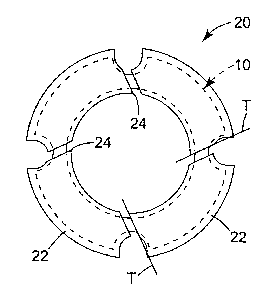
blocking layer 20 is shown in Figure 3, in which the perimeter of an
underlying signal
producing layer 10 is shown in ghost lines to illustrate the relative
arrangement of the
two layers in a finished EAS marker. Note that the signal blocking layer is
preferably
slightly larger than the signal producing layer, which helps to deactivate the
signal
producing layer.
The signal blocking layer includes signal blocking elements 22 that
generally overlie each flux collection portion 12, and are preferably but not
necessarily
discrete from each other. That is, the signal blocking layer may include two
or more
I 5 discrete signal blocking elements 22, or two or more signal blocking
elements that are
formed in a contiguous arrangement. Each signal blocking element has at least
one
boundary that generally overlies a magnetic switching section, and in the case
of the
signal blocking elements shown in Figure 3, each such element has a boundary
that
overlies two magnetic switching sections. In a preferred embodiment, at least
one of the
boundaries that overlies a magnetic switching section has a tangent "T" that
is not
perpendicular to the major axis "A" of that magnetic switching section. This
arrangement causes flux in the signal blocking element to localize at a
desired point (flux
concentration points 24, in Figure 3), and from that point to travel through
the adjacent
magnetic switching section. That flux biases the magnetic switching section
and
prevents the signal producing layer from producing a detectable signal, which
is believed
to be because the magnetic properties of the respective switching sections of
the signal
producing layer are altered, or reduced, so that the amplitude of the
alternate polarity
switching pulses from the respective elements is also significantly altered or
reduced. In
this way, the activation of the signal blocking layer prevents detection of
the signal
producing layer, and thus prevents detection of the marker. Flux concentration
points
24 are an optional, but preferred, feature of the present invention.
CA 02362679 2001-08-09
WO 00/51092 _~_ PCT/US99/14102
In the signal blocking layer embodiments shown in Figures 4 through 7,
the boundaries of adjacent discrete signal blocking elements are
complementary,
meaning that if the adjacent portions 22 were joined together they would meet
along a
single continuous line. Complementary boundaries between adjacent signal
blocking
elements are also an optional, but preferred, feature of the present
invention. Adjacent
signal blocking elements may also have non-complementary boundaries, such as
those
shown in Figure 8.
One suitable material for the signal blocking layer is an iron-based alloy
consisting of 76 weight percent iron, 20 percent nickel, and 4 percent
molybdenum,
which is commercially available from Carpenter Technology of Reading,
Pennsylvania
under the designation "MagneDur." The coercive force of MagneDur is about 45
to 65
Oersteds, and the residual magnetization is above 10,000 Gauss. Another
suitable
material for the signal blocking layer is an iron-chromium alloy consisting of
64 weight
percent iron, 6.8 percent cobalt, 28.3 percent chromium, and 0.2 percent
nickel, which is
commercially available from Arnold Engineering Company of Marengo, Illinois
under
the designation "Arnokrome 3." The coercive force of Arnokrome 3 ranges from
50 to
200 Oersteds, and the residual magnetization is also above 10,000 Gauss. Other
magnetic materials which are suitable as signal blocking layer include
Vicalloy,
Chromindur II, or the like, as known to those of ordinary skill in the art.
III. The Marker
A marker of the present invention is typically used as a dual status
marker, meaning that the marker may be activated and deactivated, preferably
repeatedly. The marker is said to be activated when the signal blocking layer
is
demagnetized, because the signal producing layer will generate a high harmonic
signal
that is detectable by conventional magnetic interrogation systems such as
those available
from the Minnesota Mining and Manufacturing Company of St. Paul, Minnesota (3M
Company). The marker is said to be deactivated when the signal blocking layer
is
magnetized, because the signal blocking layer generates sufficient magnetic
flux to
substantially saturate, or lock up, the switching section of the signal
producing layer,
thus preventing detection of the marker. Markers may be deactivated as is
known in the
CA 02362679 2001-08-09
WO 00/51092 _g_ PCT/US99/14102
art by, for example, passing the marker over a permanent magnet having a
substantially
uniform magnetic field of a single polarity. To activate the marker again, the
marker
may be passed over an alternating magnetic field of decaying amplitude, as is
known in
the art, to demagnetize the signal blocking layer.
A particular advantage of the inventive marker is that it may be
desensitized by the application of a desensitizing field applied at any
orientation relative
to the marker. More specifically, the desensitizing field may be applied at
any
orientation relative to the signal blocking layer to deactivate the marker.
Markers of this
type are said to be "multi-directionally responsive." This characteristic is
not always
true of conventional markers, but is believed to be true of the markers of the
present
invention based on tests that show complete deactivation of the marker
The parameters of the signal producing layer and the signal blocking
I S layer, and specifically the relationship between the two near the magnetic
flux areas may
be described with reference to Figure 9, in which the signal blocking layer
overlies the
signal producing layer. As shown therein, the width of the narrow region W,~
of the
signal blocking layer is preferably slightly larger than the width of the
switching section
Ws of the signal producing layer. The gap GN between adjacent portions of the
signal
blocking layer in the narrow region is not critical, but is preferably larger
than the width
of the switching section Ws for the signal producing layer, and smaller than
the length of
the switching section of the signal producing layer Ls. The length Ls is
measured
between the lines perpendicular to the switching section at which the width of
the
switching section becomes more than 5 times larger than the minimum width of
the
switching section. In the embodiment shown in Figure 9, Ls is approximately
4.1 mm
(0.16 in), WN is approximately 2.0 mm (0.08 in), Ws is approximately 0.76 mm
(0.03
in), and G,~ is approximately 1.52 mm (0.06 in). Other suitable dimensions may
be
selected to provide a marker with the desired properties and performance.
The thickness of the signal blocking layer is also preferably greater than
or equal to that of the signal producing layer, and the outer diameter of the
signal
blocking layer is preferably greater than, and the inner diameter less than,
the signal
CA 02362679 2001-08-09
WO 00/51092 _9_ PCT/US99/14102
producing layer. This enables the signal blocking layer to deactivate the
signal
producing layer, and thus the entire marker, more reliably. In a preferred
embodiment as
shown in Figures 1 through 3, the signal producing layer could be made of a
sheet of
permalloy, 0.01524 mm (0.0006 in) thick. The corresponding signal blocking
layer could
preferably be made of a sheet of MagneDur, 0.0381 mm (0.0015 in) thick.
Although both the signal producing layer and the signal blocking layer,
and thus the marker itself, may be made in any suitable size, it is preferred
to make the
marker small enough to fit within the non-recorded area (the hub) of an
optical disc.
Those dimensions, for one common type of disc, are an outer diameter of 46 mm
(1.81
in) and an inner diameter of 1 S mm (0.59 in).
To apply the marker to an object, such as an optically recorded medium,
an adhesive that adheres to but is inert relative to the object is preferably
provided on a
surface of the marker. One such adhesive is available from 3M Company under
the
designation 9461P Transfer Adhesive. Other adhesives that do not significantly
adversely affect the performance or appearance of the object may also perform
satisfactorily.
The marker may also be provided with a print receptive layer, which can
be printed with indicia such as a logo or alphanumeric information designating
the owner
or source of the article to which the marker is attached.
IV. Manufacturing the Marker
The marker of the present invention may be manufactured in any suitable
manner by, for example, laminating signal producing and signal blocking layers
together,
or by etching signal producing and signal blocking layers on opposed sides of
a single
substrate. These methods are described in greater detail below.
A. Laminating: One method of making the markers of the present
invention is by forming the signal producing and signal blocking layers
separately, and
then laminating them together in registration. For example, a sheet of
suitable material
CA 02362679 2001-08-09
WO 00/51092 PCT/US99/14102
-10-
may be stamped or otherwise formed in the pattern shown in Figure 10 to make
the
signal producing layers for many adjacent markers, and another sheet of
suitable material
may be stamped or otherwise formed in the pattern shown in Figure 11 to make
the
signal blocking layer for those markers. The two sheets can then be adhesively
or
otherwise laminated together in registration, and die cut along the
illustrated ghost lines
to provide a marker that resembles the one shown in Figure 3. The markers may
then be
cut into strips as shown in Fig. 12, and provided in a manner suitable for
dispensing.
B. Etching: Another method of making the marker of the present
invention is to laminate signal producing layer material (such as permalloy)
and signal
blocking layer material (such as MagneDur) onto opposite surfaces of a sheet
of
polymeric material (preferably a 0.001 inch thick polyester). The sheets may
be
laminated together with a 0.0254 mm (0.001 in) thick layer of a transfer
adhesive
manufactured by Minnesota Mining and Manufacturing Company (3M).
IS
After lamination, both signal producing layer and signal blocking layer
surfaces may be coated with a layer of acid resist material of a desirable
pattern, such as
those shown in Figures 10 and 11, respectively. The laminate may then be
appropriately
processed to remove the portions of the respective metal sheets that are not
covered by
the resist, such as by a conventional acid etching treatment that etches away
the exposed
metal surfaces from each of the respective layers, leaving behind the portions
of the
metal layers covered by the resist material. When the acid resist material is
removed, an
EAS marker results.
The choice of the etchant depends on the materials used as signal
producing and signal blocking layers. The suitable etchants for permalloy and
MagneDur include phosphoric acid ( H3P04), ferric chloride (FeCl3), and mixed
acids,
(see CRC Handbook of Metal Etchants, edited by Perrin Walker and William H.
Tarn,
CRC Press, 1991), or mixture of nitric Acid (1 part) and acetic acid (1 part),
or aqua
regia (nitric acid (1 part) and hydrochloride acid (3 part)). (see Smithells
Metals
References Book, edited by E.A. Brandes and G.B. Brook, 7th ed. Butterworth
CA 02362679 2001-08-09
WO 00/51092 _ 11 _ PCT/US99/14102
Heinmann, 1992). One preferred etchant used in this invention is a mixture of
ferric
chloride, hydrochloric acid, and ammonium chloride solution.
The choice of the etching process depends on the materials used as signal
producing and signal blocking layers. For example, the signal producing layer
may be a
0.0006 inch thick permalloy and the sheet of signal blocking layer may be a
0.001 S inch
thick MagneDur, and each sheet may require different exposure to etching
conditions to
remove the exposed metal. If a single etching bath is used, the combined
laminate layers
may be first exposed for a shorter period to remove the thinner permalloy. The
laminate
may then be removed from the bath and the permalloy covered to protect that
layer from
further etching. The laminate may then be reinserted into the etching bath and
etching
continued until the undesirable portions of the signal blocking layer are
removed.
The resulting patterned laminate may then be formed into a final EAS
marker by adhering a layer of printable paper or label stock over the signal
blocking
layer to form a printable surface, and by adding a layer of transfer adhesive
and a release
liner to the exposed side of permalloy sheet. The final laminate may then be
subject to
the die-cut to produce the desirable marker geometry. The undesirable weed may
then
be peeled off to leave only the final EAS markers on the release liner. For
example, dual
status EAS markers for optically-recorded media could be produced by punching
rings
having an outer diameter of 41 mm (1.625 in) and an inner diameter of 16 mm
(0.625
in).
V. Detection of the Marker
The detection systems may be amplitude detection systems, which
respond to a signal of a certain amplitude, or phase sensitive detection
systems, which
respond to a certain signal profile. To deactivate a marker so that neither
system can
detect it, the marker must produce a signal that has both an amplitude below
the
detection limit of the amplitude detection system, and a signal that does not
match the
signal profile expected by the phase sensitive detection system. Amplitude
detection
systems are available from 3M under the designations 1850, 1360, and 2300.
Detection
systems that detect phase, polarity, and amplitude are available from 3M under
the
CA 02362679 2001-08-09
WO 00/51092 _12_ PCT/US99/14102
designations 3300 and 3800, and are often used when the amplitude of a
deactivated
marker is still sufficiently high to trigger an alarm in an amplitude
detection system. The
markers of the present invention may be completely deactivated, so that
neither type of
detection system will detect the marker, and thus either type of detection
system may be
used.
A more detailed description of a conventional detection system is
provided in U.S. Patent No. 4,967,185 (Montean), the entire contents of which
is
incorporated by reference herein. Specifically, phase sensitive detection
systems
typically include two spaced panels between which persons carrying objects
protected by
EAS markers must pass to be removed from the secured area. Field coils and
detector
coils are positioned within the panels. The field coil is powered by a
suitable oscillator
coupled through a drive amplifier, which produces a magnetic field oscillating
at a
predetermined frequency within the interrogation zone extending between the
panels.
One common frequency is approximately 10 kilohertz. The detector coil is
coupled
through a sense amplifier and filter, and then to a pair of level detectors
and to a phase
sensitive detector. The common outputs of those three detectors are coupled to
an
alarm logic network, which is basically an exclusive "AND" gate, such that an
appropriate signal from all three detectors must be present to activate an
alarm. That is,
if the signal pulses do not exceed a minimum threshold, the level detectors
(and thus the
alarm signal) will not be activated, and if the signal pulses are shifted, the
phase sensitive
detection system (and thus the alarm signal) will not be activated. In the
case of
amplitude detection systems, if the amplitude of the marker is sufficiently
low when it is
desensitized, the alarm signal also will not be activated.
If a patron carrying objects having activated markers (that is, the signal
blocking portions have been deactivated) passes between the panels, the
presence of the
markers will be detected and an alarm will be produced. Conversely, if prior
to passing
between the panels the markers are deactivated (that is, the signal blocking
portions
have been activated), no alarm will sound. The present invention may also be
understood
with regard to the following examples, which are illustrative but nonlimiting
of the
invention.
CA 02362679 2001-08-09
WO 00/51092 -13- PCT/US99/14102
Examples
Example One
A 0.0152 mm (0.0006 in) thick foil made of nickel and iron of the type
available from Carpenter Technology Company of Reading, Pennsylvania under the
designation HyMu 80, measuring about 5.1 cm (2 in) square, was laminated to a
piece
of equal or larger size of adhesive coated paper. This laminate was then
punched into a
pattern as shown in Figure 1. The punched sample was then stamped into a
concentric
ring with a 15.88 mm (0.625 in) inner diameter and a 34.93 mm (1.375 in) outer
diameter to form the signal producing layer.
The signal blocking layer was also produced by punching and shearing of
0.041 mm (0.0016 in) thick iron-chrome alloy of the type sold by the Arnold
I S Engineering Company of Marengo, Illinois under the designation "Arnokrome
3," with
a pattern as shown in Figure 3. The signal blocking layer had the same inner
and outer
diameters as a signal producing element.
The signal producing layer was then bonded to the signal blocking layer
with a transfer adhesive of the type available from 3M under the designation
Scotch
Laminating Adhesive 467MP to form a dual-status EAS marker.
The signal producing layer yielded a detectable EAS signal when the
signal blocking layer was in the demagnetized state. After the signal blocking
element
was magnetized by exposure to a 150 gauss DC magnetic field, the signal
producing
layer did not generate detectable EAS signals when subjected to interrogating
fields of
up to 15 Oersteds. The signal blocking element could be deactivated at any
orientation
relative to the deactivating field, meaning that the marker was multi-
dimensional.
Markers of the type described in this Example are believed to be useful
with interrogation systems of the type available from 3M Company under the
designation model 3800 detection system.
CA 02362679 2001-08-09
WO 00/51092 _14_ PCT/US99/14102
Example Two
A length of 0.01 S mm (0.0006 in) thick nickel-iron foil available from
Carpenter Technology company of Reading, PA was laminated to a similar length
of
0.375 mm (0.0015 in) thick nickel-iron-molybdenum foil available from
Carpenter
Technology company under the designation "MagneDur" of about the same length.
The
nickel-iron foil side was then printed with the signal producing layer pattern
shown in
Figure 1: The nickel-iron-molybdenum foil side was printed with the signal
blocking
layer pattern shown in Figure 3.
The foil laminate was chemically etched on both sides by exposing the
laminate to a ferric chloride to remove uncoated permalloy and MagneDur. With
a
proper adjustment of the rate that etchant spray was applied to each side to
match the
etching rate of the two metals, the foil laminate was etched in one pass for
30 minutes.
The resulting laminate thus included patterned signal producing and signal
blocking
layers in registration with each other. Dual status EAS markers were produced
by
punching rings having an outer diameter of 41 mm (1.625 in) and an inner
diameter of
16 mm (0.625 in). The signal producing layer yielded a detectable EAS signal
when the
signal blocking layer was in the demagnetized state. After the signal blocking
layer was
magnetized by a 150 gauss DC magnetic field, the signal producing element did
not
generate a detectable EAS signal when subjected to interrogating fields of up
to 1 S
Oersteds.
The marker of the present invention may be used with any article for
which inventory control is desired. Although described primarily with
reference to their
use on optical discs, markers of the present invention may be used on other
things that
are sold, leased, or loaned to the public. Thus, the invention shall be
limited only by the
following claims.