Note: Descriptions are shown in the official language in which they were submitted.
CA 02362704 2001-08-21
WO 00/51398 PCT/DE00/00392
Description
Time-critical routing of data to a clocked interface
with asynchronous data transmission
The invention relates to a method and a circuit
arrangement for the time-critical routing of data to a
clocked interface with asynchronous data transmission,
there being parallel transmission of data between a
physical layer, or at least one physical layer, and a
further layer in accordance with a standardized layer
model, of a ready signal which is generated by the
physical layer and which indicates or does not indicate
a data transmission request, and of a release/blocking
signal which is generated by the further layer in order
to route the data transmission and/or if appropriate of
a plurality of address signals which are generated by
the further layer. In addition, a reaction to a change
in the release/blocking signal or in the ready signal
occurs within at least one clock period.
In existing and future communication systems, in
particular communications systems operating according
to the asynchronous transfer mode (ATM), data is and
will be transmitted in a cell stream formed from cells
or IP (Internet Protocol) packets. Specifically in the
case of communications systems which operate according
to the asynchronous transfer mode, the ATM layer model
is used for functionally dividing the communications
tasks, said ATM layer model being composed, like the
OSI (Open Systems Interconnection) reference model from
a plurality of communications layers which are
independent of one another. These include the physical
layer, the ATM layer, the ATM adaptation layer (AAL)
and the user-oriented layers designated as "higher
layers" in the OSI terminology. The function of a layer
is to make available services for the next higher
layer. In particular, the physical layer makes
available a transmission
CA 02362704 2001-08-21
WO 00/51398 PCT/DE00/00392
- - 2 _
interface for the cells of the superordinate ATM layer.
This interface has been defined by the ATM forum as a
uniform, clocked interface between the physical layer
and the higher layers of communications devices which
operate according to the asynchronous transfer mode,
said interface being known in the specialist field by
the name "Universal Test and Operation PHY-interface
for ATM" or "Utopia" for short - see in particular ATM
Forum, Level 2, v1.0, June 1995, pages 8-15 and 21-24.
In this UTOPIA Level 2 interface which is standardized
by the ATM Forum, during the routing of the data to the
interface very critical signaling occurs which gives
rise to a number of technical implementation problems,
particularly in the upstream direction, i.e. from the
physical interface - also referred to as secondary side
- to the communications system - also called primary
side. Inter alia, the UTOPIA specification requires,
for example, setup times of at least 4 nsec for a
50 MHz UTOPIA interface and hold times of at least
1 nsec. Owing to these setup and hold time
requirements, all the signaling signals must be sampled
at the input end immediately in order to be able to
initiate the reaction to the signaling signals in the
subsequent clock period, i.e. the signaling between the
primary side and the secondary side is very time-
critical. Furthermore, the standardized UTOPIA Level 2
interface standardizes a plurality of different complex
signaling operations, the processing of which requires
a complex control logic owing to their number. The
implementation of such rapid reaction times and the
implementation of the required complex control logic
requires suitable hardware support, i.e. high speed
logic modules such as ASICs (Application Specific
Integrated Circuit) or high speed, small FPGAs (Field
Programmable Gate Array) with short, internal signal
transit times.
CA 02362704 2004-O1-21
20365-4445
- 3 -
In the case of the standardized UTOPIA Level 2
interface, in particular the "Multiphysical" UTOPIA Level 2,
there is additionally provision for a plurality of physical
interfaces to be connected to the ATM layer, which requires
address decoding and control with respect to the physical
layer which is to be addressed. Furthermore, the previously
described complexity of the different signaling operations
in the case of a "multiphysical" operation of the UTOPIA
interface is considerably increased, i.e. a complex and
time-critical routing and decoding logic is necessary for
the time-critical routing of data from a plurality of
physical layers to the one ATM layer owing to the large
number of different complex signaling operations and the
selection of the physical layer which is authorized to
transmit data in each case.
The object on which the invention is based is to
improve the time-critical routing of the data to a clocked
interface with asynchronous data transmission, in particular
the interface between a physical layer, or between a
plurality of physical layers, and the ATM layer.
The central aspect of the method according to the
invention is the fact that the release/blocking signal is
indicated to the physical layer delayed by one clock period,
and that the data to be transmitted in parallel is routed a
priori to the clocked interface by the physical layer, and
that a reload signal for routing the data to the interface
in a suitably timed and clocked fashion is generated by a
logic connection of the delayed release/blocking signal and
of the ready signal which is generated by the physical
layer. The delaying of the release/blocking signal which is
generated by the further layer and the subsequent logic
connection of the delayed release/blocking signal to the
ready signal which is generated by the physical layer
CA 02362704 2004-O1-21
20365-4445
- 4 -
enables very short reaction times to be obtained in
different signaling operations. As a result, the number of
the signaling scenarios or cases standardized by the ATM
Forum is reduced to one case, i.e. the different time-
s critical signaling operations which occur during the
operation of the interface are processed by the method
according to the invention using a single, simple control
logic. This means that no additional cost-intensive, high
speed logic modules such as FPGAs for implementing a complex
control logic are necessary to implement the method
according to the invention but instead simple standard logic
modules such as gates and flipflops can be used. In
particular, the signaling requirements of future UTOPIA
standards which are already in planning, for example UTOPIA
Level 3 - see ATM Forum PHY WG, UTOPIA Level 3 Baseline
Text, December 1998 - with maximum clock rates of virtually
104 MHz and data bus widths of 32 bits can be advantageously
realized using the method according to the invention,
especially since in the field it is considered impractical
to realize a complex control logic which is necessary to
implement the UTOPIA Level 2 and 3 Standard without the
method according to the invention with logic functions which
are currently available in ASICs or high speed, small FPGAs
owing to the extremely short signal transit times which are
required.
According to a further embodiment of the method
according to the invention, when there is a reload signal
which indicates a data transmission, further data is routed
to the interface, and when there is a reload signal which
indicates no data transmission, the currently present data
and no further data is routed to the interface. As a
result, data is routed to the interface in a particularly
advantageous way after the transmission of the currently
present data by the delayed release or blocking signal has
CA 02362704 2004-O1-21
20365-4445
_ 5 _
already taken place, i.e. further data is routed to the
interface immediately after the transmission of the
currently present data. In addition, this ensures that no
data can be reloaded from the physical layer to the clocked
interface without a ready signal which indicates a data
request or a reload signal which indicates a data release.
The logic connection of the delayed
release/blocking signal and of the ready signal generated by
the decentralized device is advantageously carried out
according to the invention by means of a logic AND
connection. A logic AND connection constitutes a "high
speed" logic connection and can be implemented easily, i.e.
without a large degree of expenditure on circuitry.
A significant advantage of the method according to
the invention is that the data to be transmitted is routed a
priori to the clocked interface by the physical layer
without a data transmission release of the physical layer
being indicated by the further layer using the
release/blocking signal. As a result of premature routing
of the data to be transmitted to the interface by the
physical layer, data is already present a priori at the
interface, i.e, from the point of view of the physical layer
data is already being transmitted. However, ultimately the
delayed release/blocking signal directly brings about a data
transmission, i.e. when a release/blocking signal which
indicates a data transmission is present the currently
present data is transmitted and further data is routed to
the interface. The method according to the invention thus
complies with the reaction time required for data to be
applied to the interface after reception of the release and
blocking signal which indicates a data transmission.
The central aspect of the further method according
to the invention is the fact that the release/blocking
CA 02362704 2004-O1-21
20365-4445
- 6 -
signal is indicated to the physical layer delayed by at
least one clock period, and that the address signals are
delayed by at least one clock period and the ready signal
which is to be indicated to the further layer at a given
time is selected by reference to the delayed address signals
and routed to the interface. Furthermore, the data which is
to be transmitted in parallel is routed from the respective
physical layer to the clocked interface a priori and as a
function of the address signals and the release/blocking
signal, and immediately sampled. In addition, at least one
first and one second reload signal for routing the data to
the interface in a suitably timed and clocked fashion are
generated by respective logic connections of the delayed
release/blocking signal and of the delayed address signals
for a physical layer in each case. As a result of the
delaying of the release/blocking signal generated by the
further layer, and of the address signals, very short
reaction times are obtained for different signaling
operations, especially since, when the release/blocking
signal does not signal a data transmission, the physical
layer which is authorized for transmission at a given time
is determined by reference to the address signals which are
present, and said physical layer directly routes its first
data byte to the interface. The data, currently selected on
the basis of the address signals, of the respective physical
layer is thus directly present at the interface, as a result
of which the short reaction times which are required by the
UTOPIA interface standard can be realized. As a result, the
multiplicity of signaling scenarios or cases which are
standardized by the ATM Forum is reduced to a small number
of cases, i.e. the different, time-critical signaling
operations which occur during the operation of the interface
and the selection of the respective physical layer are
processed by the method according to the invention using a
single simple routing and decoding logic. This means that,
CA 02362704 2004-O1-21
20365-4445
in order to implement the method according to the invention,
no cost-intensive, high speed logic modules, such as high
speed ASICs or small, high speed FPGAs are necessary to
implement a complex routing and decoding logic, but rather
it is possible to use simple, cost-effective, relatively
slow ASICs or FPGAs. In particular, the signaling
requirements of future UTOPIA standards which are already in
planning, for example MPHY-UTOPIA Level 3 - see ATM Forum
PHY WG, UTOPIA Level 3 Baseline Text, December 1998 - with
maximum clock rates of virtually 104 MHz and data bus widths
of 32 bits can be advantageously implemented using the
method according to the invention, especially since an
implementation of a complex control logic which is necessary
to implement the UTOPIA level 2 and 3 Standard, in
particular in the case of "multiphysical" operation is
considered to be impractical in the specialist field without
the method according to the invention with logic functions
which are currently available in ASICs or high speed, small
FPGAs, owing to the extremely short signal transit times
which are required.
According to a further refinement of the further
method according to the invention, when there is a first
reload signal which indicates a data transmission previously
stored data is routed to the interface, and when there is a
second reload signal which indicates a data transmission
further data is routed to the interface. Furthermore, when
there is a first or second reload signal which indicates no
data transmission, the currently present data and no further
data is routed to the interface, and data is routed to the
interface either using the first or the second reload
signal. As a result, the data to be transmitted is routed
to the interface in a particularly advantageous way, in
particular after the transmission of the currently present
data by the delayed release/blocking signal has already
CA 02362704 2004-O1-21
20365-4445
_ g _
taken place, i.e. further data is routed to the interface
immediately after the transmission of the currently present
data. In addition, this ensures that no data is reloaded
from the physical layer to the clocked interface without a
ready signal which indicates a data request or a first or
second reload signal which indicates a data release.
Furthermore, data which has already been stored in a memory
unit is advantageously routed by the first reload signal,
i.e. for example the first data word or data byte of an ATM
cell, or the cell start signal which is present, is buffered
in a memory unit in the current clock cycle and read out in
the next clock cycle if requested and routed directly to the
interface. In this way, data which is required in the next
clock period and is no longer currently present can be
particularly advantageously routed at short notice to the
interface, as a result of which, for example, the loss of a
data byte or of an information item which is present in the
current clock period but is required at a given time is
avoided.
The logic connections of the delayed
release/blocking signal and of the delayed and decoded
address signals for a physical layer in each case is
advantageously carried out according to the invention using
a decoding unit, i.e., the advantageous embodiment can be
implemented without a large degree of expenditure on
circuitry. Furthermore, the signal transit times are kept
short by implementing the decoding unit on a single logic
level.
An essential advantage of the further method
according to the invention is that data, to be transmitted,
of the physical layer selected by reference to the address
signals is routed a priori to the clocked interface from the
respective physical layer without the further layer
CA 02362704 2004-O1-21
20365-4445
_ g _
indicating a data transmission release for the respective
physical layer using the release/blocking signal by
reference to the address signals generated by the further
layer for addressing the respective physical layer. By
virtue of the premature routing of the data to be
transmitted from the respective physical layer to the
interface, data is already present a priori at the
interface, i.e, from the point of view of the respective
physical layer data is already being transmitted; but the
delayed release/blocking signal directly brings about a data
transmission, i.e. when a release/blocking signal which
indicates a data transmission is present, the data which is
currently present is transmitted and further data is routed
to the interface. The method according to the invention
thus ensures the short reaction time which is required for
the application of data of the physical layer defined by the
address signals to the interface after reception of the
release/blocking signal which indicates a data transmission.
In accordance with one aspect of this invention,
there is provided a method for the time-critical routing of
data to a clocked-interface with asynchronous data
transmission, comprising: parallelly transmitting data
between a physical layer and an ATM layer in accordance with
a standardized layer model, of a ready signal which is
generated by the physical layer and indicates or does not
indicate a data transmission request, and of a
release/blocking signal which is generated by the ATM layer
to route the data transmission; and reacting to a change in
the release/blocking signal or in the ready signal within at
least one clock period, wherein the release/blocking signal
is indicated to the physical layer delayed by one clock
period, and the data which is to be transmitted in parallel
is routed a priori to the clocked interface by the physical
layer, and a reload signal for routing the data to the
CA 02362704 2004-O1-21
20365-4445
- 9a -
interface in a timed and clocked fashion is generated by a
logic connection of the delayed release/blocking signal and
of the ready signal which is generated by the physical
layer.
In accordance with another aspect of this
invention, there is provided a circuit arrangement for the
time-critical routing of data to a clocked interface with
asynchronous data transmission, comprising: a first control
unit provided in one physical layer and a second control
unit provided in an ATM layer; a transmission device for the
parallel transmission of data from the physical layer to the
ATM layer and for transmitting a ready signal which is
generated by the physical layer and indicates or does not
indicate a data transmission request, and a release/blocking
signal which is generated by the ATM layer; a reaction
device to react to a change in the release/blocking signal
or in the ready signal within at least one clock period; a
delay device for delaying the release/blocking signal for a
length of one clock period and for passing on the delayed
release/blocking signal to the physical layer; a logic
connecting device for logically connecting the delayed
release/blocking signal and the ready signal generated by
the physical layer to form a reload signal and for passing
on a reload signal to the physical layer.
In accordance with yet another aspect of this
invention, there is provided a method for time-critical
routing of data to a clocked MPh-Utopia interface with
asynchronous data transmission, comprising: parallelly
transmitting data between at least one physical layer and
one ATM layer in accordance with a standardized layer model,
of at least one ready signal which indicates or does not
indicate a data transmission request which is generated by a
physical layer in each case, of a release/blocking signal
CA 02362704 2004-O1-21
20365-4445
- 9b -
which is generated by the ATM layer to control the data
transmission, and of a plurality of address signals which
are generated by the ATM layer to address the respective
physical layer; reacting to a change in the release/blocking
signal within at least one clock period; indicating the
release/blocking signal to the physical layer delayed by at
least one clock period; delaying the address signals by at
least one clock period and the ready signal which is to be
indicated to the ATM layer at a given time is selected by
reference to the delayed address signals and routed to the
clocked MPh-Utopia interface; routing the data which is to
be transmitted in parallel from the respective physical
layer to the clocked MPh-Utopia interface a priori and as a
function of the address signals and the release/blocking
signal, and immediately sampled; and generating at least one
first and one second reload signal for routing the data to
the MPh-Utopia interface in a suitably timed and clocked
fashion by respective logic connections of the delayed
release/blocking signal and of the delayed and decoded
address signals for a physical layer in each case.
In accordance with yet a further aspect of this
invention, there is provided a circuit arrangement for the
time-critical routing of data to a clocked MPh-Utopia
interface with asynchronous data transmission, at least a
first control unit being provided in at least one physical
layer and a second control unit being provided in an ATM
layer, comprising: a device for the parallel transmission of
data from at least one of the physical layers to the ATM
layer and for the transmission of a ready signal which is
generated by a physical layer in each case and indicates or
does not indicate a data transmission request, and of a
release enable signal which is generated by the ATM layer
and of a plurality of address signals which is generated by
the ATM layer to address the respective layer; a reaction
CA 02362704 2004-O1-21
20365-4445
- 9c -
device to react to a change in the release/blocking signal
or at least in a ready signal within at least one clock
period; a first delay element for delaying the
release/blocking signal for at least the length of a clock
period and for forwarding the delayed release/blocking
signal to the physical layer; a second delay element for
delaying the address signals for at least the length of a
clock period and for forwarding the delayed address signals
to the physical layer and a decoding device for decoding the
address signals; and a logic connection device for logically
connecting in each case the delayed lock signal and the
delayed and decoded address signals are logically connected
to form in each case a first and second reload signal for a
physical layer in each case, and for forwarding the first
and second reload signals to the respective physical layer.
The invention is explained in more detail below
with reference to two block circuit diagrams and two signal
flowcharts.
Figure 1 is a block circuit diagram showing a
circuit arrangement developed for implementing the method
according to the invention.
Figure 2 shows the signal flow, characterizing the
method according to the invention, at the clocked interface,
Figure 3 is a block circuit diagram showing a
circuit arrangement according to the invention of a
"multiphysical" UTOPIA interface, and
Figure 4 shows the signal flow at the clocked
"multiphysical" UTOPIA interface.
CA 02362704 2004-03-10
20365-4445
- 9d -
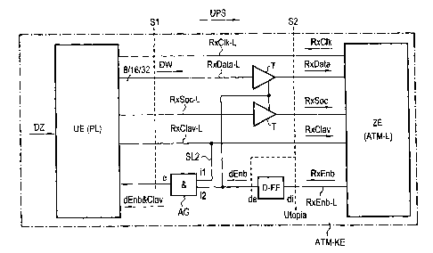
The block circuit diagram according to Figure 1 shows
an ATM communications device ATM-KE which operates
according to the asynchronous transfer mode, with a
CA 02362704 2001-08-21
WO 00/51398 PCT/DE00/00392
- 10
transmission unit UE which implements a physical layer
PL, and an access unit ZE which implements an ATM layer
ATM-L, the physical layer PL providing the transmission
equipment which is necessary for the transmission of
data cells DZ, and the ATM layer ATM-L having higher
network protocols for the functional separation of
communications functions. In particular, Figure 1 shows
a possible implementation of the Utopia interface,
standardized by the ATM Forum, between the physical
layer PL and the ATM layer ATM-L - also referred to as
UTOPIA interface, the circuit arrangement according to
the invention and/or the method according to the
invention relates specifically to the time-critical
routing of data cells DZ to the clocked Utopia
interface for parallel transmission in the upstream
direction UPS. Here, the upstream direction UPS is to
be understood as the parallel transmission of data
cells DZ starting from the physical layer PL to the ATM
layer ATM-L. For the parallel transmission of the data
cells DZ, they are divided into data words DW, each
with a length of 8, 16 or 32 bits, and subsequently a
single data word DW1 per clock period Fx is transmitted
in parallel, a clock period Fx comprising in each case
the period between two successive rising clock edges
F1-F8. Furthermore, the interface lines RxClk-L,
RxData-L, RxSoc-L, RxClav-L, RxEnb-L which are provided
for the implementation of the UTOPIA interface defined
by the ATM Forum are illustrated in Figure 1. Here, the
clock signal RxClk is transmitted via the clock signal
interface line RxClk-L, the data signal RxData is
transmitted via the data signal interface line
RxData-L, the cell start signal RxSoc is transmitted
via the cell start signal interface line RxSoc-L, the
ready signal RxClav is transmitted via the ready signal
interface line RxClav-L, and the release/blocking
signal RxEnb is transmitted via the release or blocking
signal interface line RxEnb-L, the respective direction
of the signal transmission being defined by the
directions of the arrows given in Figure 1.
CA 02362704 2001-08-21
WO 00/51398 PCT/DE00/00392
- 11
The superordinate or controlling entity within the
clocked interface is formed, as illustrated by way of
example in Figure 1, by the ATM layer ATM-L, i.e. the
parallel data transmission is routed, and the data
transmission started or terminated, by the ATM layer
ATM-L using the release/blocking signal RxEnb.
Furthermore, the physical layer PL which is subordinate
to the ATM layer ATM-L routes the data to be
transmitted in the form of data cells DZ or data words
DW to the clocked interface Utopia, in which case, on
the one hand, the ATM layer ATM-L makes the physical
layer PL prepare data words DW, but on the other hand
data words DW are routed to the interface even without
a data request by the physical layer PL to the ATM
layer ATM-L. The transmission of the data words DW from
the physical layer PL to the ATM layer ATM-L is carried
out using the data signal RxData, via which one 8-bit,
16-bit or 32-bit data word DW can be transmitted per
clock period Fx. Furthermore, the ATM layer ATM-L
indicates or predefines to the physical layer PL the
clock rate for the clocked, parallel data transmission
by the clock signal RxClk. In addition, a cell start
signal RxSoc is provided on a standard basis for the
implementation of the Utopia interface and is used by
the physical layer PL to indicate to the ATM layer ATM-
L the start of a new data cell , i . a . in particular the
transmission of the first data word DW1 of a data cell.
This means that during parallel transmission of the
first data word DW1 of a data cell, from the point of
view of the ATM layer ATM-L the cell start signal RxSoc
which has the logic value "0" is set to the logic value
"1" for the duration of one clock period Fx, and as a
result the start of a data cell is signaled to the ATM
layer ATM-L. If data is present, or even if no data is
present, for parallel transmission to the ATM layer
ATM-L in the physical layer PL, this is indicated to
the ATM layer ATM-L using the ready signal RxClav. In
order to implement the method according to the
CA 02362704 2001-08-21
H10 00/51398 PCT/DE00/00392
' - 12 -
invention, a delay means D-FF, for example a D-flipflop
for delaying the release/blocking signal RxEnb
generated by the ATM layer ATM-L for routing the data
transmission is provided, the release/blocking signal
RxEnb which is generated by the ATM layer ATM-L being
routed to the input di of the delay means D-FF using
the release and blocking signal interface line RxEnb-L,
and the release/blocking signal dEnb which is delayed
by one clock period Fx being present at the output de
of the delay means D-FF.
In compliance with the UTOPIA interface standard,
tristate driver modules T which act in the upstream
direction UPS with respect to the Utopia interface are
provided for connecting through the cell start signal
RxSoc and the data signal RxData to the ATM layer
ATM-L, as shown in Figure 1. The tristate driver
modules T can route the cell start signal interface
line RxSoc-L and the data signal interface line RxData-
L into the "tri-stated" or "high impedance" state, and
the transmission of the cell start signal RxSoc or of
the data signal RxData can thus be prevented. This is
the case in particular if no data transmission of the
superordinate ATM layer ATM-L is provided, and the
tristate driver modules T can thus be made, using the
delayed release/blocking signal dEnb transmitted via a
first control line SL1, to change the cell start signal
interface line RxSoc-L and the data signal interface
line RxData-L into the "tri-stated" state.
A logic connecting means AG, for example an AND gate,
is provided for implementing the logic connection,
according to the invention, of the ready signal RxClav
and of the delayed release/blocking signal dEnb. The
ready signal RxClav is routed, using the second control
line SL2, to the first input il of the logic connecting
means AG, said input il being connected via a second
control line SL2 to the ready signal interface line
RxClav-L, and
CA 02362704 2001-08-21
~nTO 00/51398 PCT/DE00/00392
- 13
the delayed release/blocking signal dEnb is routed,
using the release or blocking signal interface line
RxEnb-L, to the second input i2 which is connected to
the output de of the delay means D-FF via the release
or blocking signal interface line RxEnb-L, and after
the AND connection of the two signals a reload signal
dEnb&Clav for routing the data words DW to the Utopia
interface in a suitably timed and clocked fashion is
present at the output a of the logic connecting means
AG. The reload signal dEnb&Clav indicates to the
physical layer PL that a further data word DW can be
routed to the Utopia interface.
The signal flow which occurs during the time-critical
routing, according to the invention, of data words DW
to the clocked interface is illustrated in Figure 2 by
means of individual signal flowcharts. In compliance
with the UTOPIA interface standard, the signaling
signals RxClk, RxData, RxSoc, RxClav, RxEnb are each
sampled after a rising clock pulse edge F1-F8, for
example a first, second, third, fourth, fifth, sixth,
seventh and eighth rising clock pulse edge F1-F8 being
illustrated in Figure 2. In order to explain the method
according to the invention, eight clock periods Fx are
shown between the first and eighth positive clock edge
F1-F8, an individual clock edge F1-F8 being indicated
in each case by a dotted line. Furthermore, Figure 2
shows the signal profiles of the signaling signals
RxClk, RxData, RxSoc, RxClav, RxEnb, dEnb, dEnb&Clav
immediately after the physical layer PL - expressed in
Figure 1 by a dot-dashed line designated by S1 - and at
the Utopia interface - expressed in Figure 1 by a
dashed line designated by S2 or Utopia - and are
referred to below as first interface S1 and as second
interface S2. The signal profiles in the plane S1
and/or S2 of the clock signal RxClk, of the data signal
RxData, of the cell start signal RxSoc, of the ready
signal RxClav, of the release/blocking signal RxEnb, of
the delayed
CA 02362704 2001-08-21
WO 00/51398 PCT/DE00/00392
- 14
release/blocking signal dEnb and of the reload signal
dEnb&Clav are explained in more detail by Figure 2.
At the time of the first rising clock pulse edge F1,
the ready signal RxClav, having the logic value "0", of
the ATM layer ATM-L indicates that at that time there
are no data words DW available for parallel
transmission in the physical layer PL. Analogously, the
data signal RxData at the first interface S1 does not
indicate the presence of any data words DW and owing to
the release/blocking signal RxEnb which does not
indicate any data transmission and which has the logic
value "1", both the data signal RxData and the cell
start signal RxSoc are changed to the "tri-stated"
state at the second interface S2 or Utopia interface
using the tristate driver modules T at the time of the
first rising clock pulse edge F1. This means that the
data transmission to the ATM layer ATM-L is
interrupted. Correspondingly, the delayed
release/blocking signal dEnb has a logic value "1" - no
data transmission - and the reload signal dEnb&Clav has
a logic value "0", by which a release of the UTOPIA
interfaces, i.e. data words DW can be routed to the
UTOPIA interface, is indicated to the physical layer
PL.
At the time of the second rising clock pulse edge F2,
the cell start signal RxSoc is set to the logic value
"1" by the physical layer PL at the first interface S1,
and the start of a data cell DZ or the presence of a
first data word DW1 in the physical layer PL is thus
indicated. In contrast, the cell start signal interface
line RxSoc-L is still kept in the "tri-stated" state at
the second interface B by the tristate driver module T,
and the transmission of the cell start signal RxSoc to
the ATM layer ATM-L is thus suppressed. Furthermore,
the first data word DW1 is routed to the first
interface S1 using the data signal RxData,
CA 02362704 2001-08-21
WO 00/51398 PCT/DE00/00392
- 15
the data signal interface line RxData-L being also
still held in the "tri-stated" state here again at the
second interface S2 by the tristate driver module T.
The physical layer PL signals a data transmission
request to the ATM layer ATM-L, or indicates readiness
to transmit data, by means of the ready signal RxClav
present in unchanged form at both the first and second
interfaces. The ready signal RxClav is kept constant
over the following six periods, i.e. signals a data
transmission request. The release/blocking signal
RxEnb, and consequently the delayed release/blocking
signal dEnb, continue to have an unchanged logic value
"1" at the second interface B - no data transmission.
In contrast, the logic value of the reload signal
dEnb&Clav has changed from "0" to "1", after which the
physical layer PL can no longer reload any data words
DW to the Utopia interface, i.e. only the currently
present first data word DW1 is made available for the
transmission.
At the time of the third rising clock edge F3, the
previously mentioned signal profiles remain unchanged
with the exception of the release/blocking signal RxEnb
which is present at the second interface S2, by means
of which the ATM layer ATM-L reacts to the change,
occurring one clock period Fx before; in the ready
signal RxClav which indicates a data transmission
request. As a result, the ATM layer ATM-L carries out a
release, using the release/blocking signal RxEnb, for
the transmission of data via the Utopia interface.
This release for the transmission of data becomes
effective at the time of the fourth rising clock pulse
edge F4 owing to the release/blocking signal dEnb
delayed at the switching interface S2, i.e. a delayed
release/blocking signal dEnb with a logic value "0" is
present, which, using the tristate driver modules T,
releases the first data word DW1 for transmission.
Consequently, the first data
CA 02362704 2001-08-21
WO 00/51398 PCT/DE00/00392
- 16
word DW1 at the second interface S2 is then transmitted
to the ATM layer ATM-L using the RxData data signal,
the start of the data cell being signaled to the ATM
layer ATM-L simultaneously by the cell start signal
RxSoc. Furthermore, the reload signal dEnb&Clav at the
first interface S1 has a change in the logic value from
"1" to "0". This means that for example a second data
word DW2 can be reloaded to the UTOPIA interface by the
physical layer PL in the following clock period Fx.
At the time of the following fifth clock pulse edge F5,
the cell start signal RxSoc is reset to the logic value
"0" and assumes this logic value without change until
the transmission of a further data cell takes place.
The second data word DW2 is transmitted to the ATM
layer ATM-L in the upstream direction UPS using the
data signal RxData. Analogously, the third and fourth
data words DW3, DW4 are transmitted in the respective
following clock period Fx.
The block circuit diagram according to Figure 3 shows,
by analogy with Figure 1, an ATM communications device
ATM-KE which operates according to the asynchronous
transfer mode, with a first transmission unit UE1 which
implements a first physical layer PL1, a second
transmission unit UE2 which implements a second
physical layer PL2 and an access unit ZE which
implements the ATM layer ATM-L, the first and second
physical layers PL1, PL2 providing the transmission
equipment which is necessary for the transmission of
data cells DZ, and the ATM layer ATM-L having higher
network protocols for the functional separation of the
communications functions. In particular, Figure 3 shows
a possible way of implementing the Utopia Level 2
interface which is standardized by the ATM Forum
between, for example, the first and second physical
layer PL1, PL2, and the ATM layer ATM-L - also referred
to as "multiphysical" - UTOPIA interface,
CA 02362704 2001-08-21
WO 00/51398 PCT/DE00/00392
- 17
the circuit arrangement or the method according to the
invention specifically relating to the time-critical
routing of data cells DZ to the clocked MPh-Utopia
interface for parallel transmission in the upstream
direction UPS. In particular, for example the first and
second physical layers PL1, PL2 are illustrated in
Figure 3, the method according to the invention being
applicable for routing data of any desired number of
physical layers PL1, PL2 to the ATM layer ATM-L. Here,
by analogy with Figure 1, the upstream direction UPS is
to be understood to mean the parallel transmission of
data cells DZ starting from one of the physical layers
PL1, PL2 to the ATM layer ATM-L. Furthermore, Figure 3
shows in turn the interface lines RxClk-L, RxData-L,
RxSoc-L, RxClav-L, RxEnb-L, RxAdrl, RxAdr2 provided for
implementing the "multiphysical" UTOPIA interface
defined by the ATM Forum, the first and second address
signals RxAdrl/RxAdr2 being additionally transmitted
via a first and second address signal interface line
RxAdrl/RxAdr2 in order to implement the "multiphysical"
Utopia MPh-Utopia interface. Here too, the arrows
illustrated in Figure 3 represent the respective
direction of the signal transmission.
The superordinate or controlling entity within the
clocked interface is formed, by analogy to Figure 1, by
the ATM layer ATM-L as illustrated by way of example in
Figure 3, i.e. using the release/blocking signal RxEnb
and the first and second address signals RxAdrl/RxAdr2,
the ATM layer ATM-L routes the parallel data
transmission and/or selects the first or second
physical layer PL1, PL2 and starts or terminates the
data transmission. Furthermore, the first and second
physical layers PL1, PL2 which are subordinate to the
ATM layer ATM-L route the data to be transmitted in the
form of data cells DZ or data words DW to the clocked
MPh-Utopia interface, in which case,
CA 02362704 2001-08-21
WO 00/51398 PCT/DE00/00392
- 18 -
on the one hand, the ATM layer ATM-L makes the
respective first or second physical layer PL1/PL2
prepare data words DW, but on the other hand the first
or second physical layer PL1, PL2 routes data words DW
to the interface even without a data request to the ATM
layer ATM-L. The data words DW are transmitted from the
first or second physical layer PL1, PL2 to the ATM
layer ATM-L using the data signal RxData via which one
8-bit, 16-bit or 32-bit data word DW per clock period
Fx can be transmitted. Furthermore, by analogy to
Figure 1, the ATM layer ATM-L can indicate or predefine
the clock rate for the clocked, parallel data
transmission both to the first and second physical
layers PL1, PL2 by means of the clock signal RxClk. In
addition, a cell start signal RxSoc is also provided on
a standard basis for the implementation of the MPh-
Utopia interface and is used by the first or second
physical layer PL1, PL2 of the ATM layer ATM-L to
indicate the start of a new data cell DZ, i.e. in
particular the transmission of the first data word DW1
of a data cell. This means that during the parallel
transmission of the first data word DW1 of a data cell,
from the point of view of the ATM layer ATM-L the cell
start signal RxSoc which has the logic value "0" is set
to the logic value "1" for the duration of one clock
period Fx and as a result the start of a data cell of
the respective physical layer PL1, PL2 which is
selected by reference to the first and second address
signals RxAdr1/RxAdr2 most recently present is signaled
to the ATM layer ATM-L. If data are present, or even if
no data are present, for parallel transmission to the
ATM layer ATM-L in the first or second physical layer
PL1, PL2, this is indicated to the ATM layer ATM-L
using the ready signal RxClav.
In order to explain the method according to the
invention, by way of example the transmission of data
CA 02362704 2001-08-21
WO 00/51398 PCT/DE00/00392
- 18a -
from the first physical layer PL1 to the ATM layer
ATM-L will be described. The transmission of data
starting from the second physical
CA 02362704 2001-08-21
WO 00/51398 PCT/DE00/00392
- 19
layer PL2 and the structure of the second transmission
unit UE2 is analogous to the first physical layer PLl
or the first transmission unit UE1 and is consequently
not described in detail below.
In order to implement the method according to the
invention, first to eleventh delay means D-FF1 - D-FF11
for example D-flipflops, are provided for delaying the
respective signals to be transmitted, all the delay
means D-FF1 - D-FF11 each having an input and output
i/e and some have an additional control input si. The
fifth, sixth and seventh delay elements D-FF5 - D-FF7
are arranged, for example, in the first transmission
unit UE1 of the first physical layer PL1. In the
exemplary embodiment according to Figure 3 which is
described in more detail, the third, fourth, sixth and
seventh delay means D-FF3/4/6/7, for example, have an
additional control input si. In addition, the first
transmission unit UE1 comprises a Utopia Level 1
interface unit UL1 for implementing the Utopia Level 1
interface, and a glue logic unit GLE for controlling
the signaling operations, defined by the UTOPIA
interface standard, of different transmission methods
or events during the transmission of ATM cells.
Furthermore, a fourth to eighth tristate driver module
T4-T8 for connecting through the respective signals and
an inverter I are provided in the first physical layer
PL1. In order to implement the selection according to
the invention of the first or second physical layer
PL1, PL2, a first and a second decoding unit DE1, DE2
and a first, second and third tristate driver module
T1-T3 for switching through the signals which are
present are provided in the ATM communications device
ATM-KE. In addition, a pull-down resistor PDR and a
logic connection means AG, for example an "AND" gate
for advantageously routing the data to the clocked MPh-
Utopia interface, are arranged in the ATM
communications device ATM-KE.
CA 02362704 2001-08-21
WO 00/51398 PCT/DE00/00392
- 20
The access unit ZE which implements the ATM layer ATM-L
is connected via the release/blocking signal interface
line RxEnb-L to the input i of a first delay means
D-FF1. The output a of the first delay means D-FF1 is
routed via a further release/blocking signal interface
line RxEnb-L to the input i of a second delay means
D-FF2, the further release/blocking signal interface
line RxEnb-L which is connected to the output a of the
first delay means D-FF1 being connected to the first
input il of the second decoding unit DE2. The output a
of the second delay means D-FF2 is connected to the
first input il of the glue logic unit GLE of the first
physical layer PL1. Analogously, the output a of the
second delay means D-FF2 is wired to the first input il
of the glue logic unit GLE of the second physical layer
PL2 - not illustrated in Figure 3. Furthermore, the
output a of the first delay means D-FF1 is also
connected to, in each case, the second input i2 of the
glue logic unit GLE of the first or second physical
layer PLl, PL2. In addition, the control input si of
the third and fourth delay means D-FF3, D-FF4 is
connected to the output a of the first delay means
D-FF1. In each case the control unit si of the second
and third tristate driver modules T2/T3 is also
connected to the output a of the first delay means
D-FF1.
The access unit ZE is connected to the input i of the
eleventh delay means D-FF11 via the first address
signal interface line RxAdrl-L. The output a of the
eleventh delay means D-FF11 is connected to the first
input il of the first decoding unit DE1 and to the
second input i2 of the logic connection means AG.
Analogously, the access unit ZE is connected to the
input i of the tenth delay means D-FF10 via the second
address signal interface line RxAdr2-L, and the output
a of the tenth delay means D-FF10 is connected both to
the second input i2 of the f first decoding unit DE1 and
to the first
CA 02362704 2001-08-21
WO 00/51398 PCT/DE00/00392
- 21
input i1 of the logic connection means AG, as well as
to the second input i2 of the second decoding unit DE2.
The output a of the logic connection means AG is itself
connected to the control input si of the first tristate
driver module T1.
The access unit ZE is additionally connected via the
clock signal interface line RxClk-L to the first and
second physical layers PL1, PL2, in particular to the
respective Utopia Level 1 interface unit UL1 in order
to transmit the clock signal RxClk from the ATM layer
ATM-L to the first or second physical layer PL1, PL2.
The first output el of the first decoding unit DE1 is
routed to the input i of the fourth delay means D-FF4
and to the inverted control input si of the fourth
tristate driver module T4. The second output e2 of the
first decoding unit DE1 is connected to the input i of
the third delay means D-FF3 and to the inverted control
input si of a tristate driver module of the second
physical layer PL2 - not illustrated in Figure 3.
Furthermore, the output a of the fourth delay means
D-FF4 is connected to the third input i3 of the glue
logic unit GLE . Analogously, the output a of the third
delay means D-FF3 is connected to the glue logic unit
GLE of the second physical layer PL2 - not illustrated
in Figure 3 either.
The first output el of the second decoding unit DE2 is
connected to the control input si of the seventh and
eighth tristate driver modules T7, T8, and the second
output e2 of the second decoding unit DE2 is connected
to the control input of the fifth and sixth tristate
driver modules T5/6 using a connecting line in each
case. Analogously, the third and fourth outputs e3/e4
of the second decoding unit DE2 are routed to control
inputs of tristate driver modules of the second
physical layer PL2,
CA 02362704 2001-08-21
WO 00/51398 PCT/DE00/00392
- 22 -
said control inputs not being illustrated in Figure 3
for reasons of clarity.
The glue logic unit GLE which is provided in the first
transmission unit UE1 has an output a which is
connected to the first input of the Utopia Level 1
interface unit UL1 and to the input i of the inverter
I. The output a of the inverter I is connected to the
control input si of the sixth and seventh delay means
D-FF6, D-FF7. The first output el of the Utopia Level 1
interface unit UL1 is connected to the input i of the
fourth tristate driver module T4 and to the fifth input
i5 of the glue logic unit GLE and to the input i of the
fifth delay means D-FFS, the output a of the fifth
delay means D-FF5 being routed to the fourth input i4
of the glue logic unit GLE.
The second output e2 of the Utopia Level 1 interface
unit UL1 is connected to the input i of the sixth delay
means D-FF6 and to the input i of the seventh tristate
driver means T7, the output a of the sixth delay means
D-FF6 being routed to the input i of the fifth tristate
driver means T5. Furthermore, a connection is provided
between the third output e3 of the Utopia Level 1
interface unit UL1 and the input i of the seventh delay
means D-FF7, the output a of the seventh delay means
D-FF7 being connected to the seventh tristate driver
module T6. In addition, the third output e3 of the
Utopia Level 1 interface unit UL1 is connected to the
input i of the eighth tristate driver module T8. The
two outputs a of the fifth and seventh tristate driver
modules T5, T7 are connected to the input i of the
eighth delay means D-FF8, the outputs of the
corresponding tristate driver means that are arranged
on the second physical layer PL2 also being connected
to the input i of the eighth delay means D-FF8. The
outputs a of the sixth and eighth tristate
CA 02362704 2001-08-21
WO 00/51398 PCT/DE00/00392
- 23
driver modules T6, T8 being connected to the input i of
the ninth delay means D-FF9, the outputs of the
corresponding tristate driver means which are arranged
on the second physical layer PL2 being in turn
connected to the input i of the ninth delay means
D-FF9. The output a of the eighth delay means D-FF8 is
connected to the input i of the second tristate driver
module T2, and the output a of the ninth delay means
D-FF9 is routed to the input i of the third tristate
driver module T3. The access unit ZE which implements
the ATM layer ATM-L is connected to the output a of the
second tristate driver module T2 via the cell start
signal interface line RxSoc-L. Furthermore, the access
unit ZE is connected to the output a of the third
tristate driver module T3 via the data signal interface
line RxData-L.
The output a of the fourth tristate driver module T4 is
connected, together with the output a of the tristate
driver module which is analogously arranged in the
second physical layer PL2 , to the input i of the f first
tristate driver module T1 which is connected to ground
via a pull-down resistor PDR. Furthermore, the control
unit si of the first tristate driver module Tl is
connected to the output a of the logic connection means
AG.
In compliance with the UTOPIA interface standard, the
first, second and third tristate driver modules T1-T3
which operate in the upstream direction UPS with
respect to the MPh-Utopia interface are, as illustrated
in Figure 3, provided for switching through the cell
start signal RxSoc or the data signal RxData or the
ready signal RxClav to the ATM layer ATM-L. The first,
second and third tristate driver modules T1-T3 can
respectively change the cell start signal interface
line RxSoc-L and the data signal interface line
RxData-L and the ready signal interface line RxClav-L
to the "tri-stated" state
CA 02362704 2001-08-21
WO 00/51398 PCT/DE00/00392
- 24
or "high impedance" state, and the transmission of the
cell start signal RxSoc or of the data signal RxData or
of the ready signal RxClav can thus be routed or
prevented. This is the case in particular if no data is
to be transmitted by the superordinate ATM layer ATM-L,
and the second and third tristate driver modules T2, T3
are thus made to change the cell start signal interface
line RxSoc-L and the data signal interface line RxData-
L to the "tri-stated" state using the delayed
release/blocking signal dEnb. Analogously, the fourth,
fifth, sixth, seventh and eighth tristate driver
modules T4-T8 which operate in the upstream direction
VPS with respect to the MPh-Utopia interface are
provided in the first physical layer PL1 in order to
switch through the signals transmitted by the first
Utopia Level 1 interface unit UL1, in particular the
first data signal RxDatal, the first cell start signal
RxSocl and the first ready signal RxClavl. Each of the
outputs between the fourth and eighth tristate driver
modules T4-T8 and the first, second and third tristate
driver modules T1-T3 can be changed to the "tri-stated"
or "high impedance" state by the fourth to eighth
tristate driver modules T4-T8, and the transmission of
the first cell start signal RxSocl or of the first data
signal RxDatal or of the first ready signal RxClavl is
thus routed or prevented. This means that the signals
of the physical layer PL1, PL2 which is selected using
the first and second address signals RxAdrl/RxAdr2 can
be routed to the interface using the fourth to eighth
tristate driver modules T4-T8, the transmission of data
being suppressed in the physical layer PL1, PL2 which
is not authorized for transmission, by the tristate
driver modules which are analogously provided on the
respective assembly.
The ATM layer ATM-L transmits, by reference to the
first and the second address signals RxAdrl, RxAdr2,
the binary address of the physical layer PL1, PL2 which
is to be addressed or a
CA 02362704 2001-08-21
WO 00/51398 PCT/DE00/00392
- 25 -
filler bit sequence F which is standardized by the ATM
Forum and transmitted in each case in the clock period
after a valid address, in which case, in the method
according to the invention, the first and second
address signals RxAdrl, RxAdr2 are switched onwards to
the first decoding unit DE1 delayed by one clock period
Fx using the tenth and eleventh delay means D-FF10/11.
The delayed first and second address signals
dAdrl/dAdr2 constitute a binary address, with the
result that, for example, the second physical layer PL2
is addressed by a first delayed address signal dAdrl
which has a logic value "0", and by a second delayed
address signal dAdr2 which has a logic value "1" , i . a .
the combination of the binary information contained in
the first and second delayed address signals
dAdrl/dAdr2 yields the binary value "10" which
corresponds to a value "2" in the decimal system. In
addition, the delayed first and second address signals
dAdrl, dAdr2 are transmitted via connecting lines to
the logic connecting unit AG and logically connected
there, for example using the "AND" gate. The first
tristate driver module T1 which switches through the
ready signal RxClav is routed by the control signal
present at the output a of the logic connecting unit
AG, the presence of the filler bit sequence F, for
example the binary value "11" which is standardized by
the ATM Forum and transmitted in each case in the clock
period after a valid address, at the inputs il, i2 of
the logic connecting unit AG causes the first tristate
driver module T1 to be changed to the "tri-stated" or
"high impedance" state. Furthermore, for example the
delayed, second address signal dAdr2 is additionally
transmitted to the second decoding unit DE2 in order to
support the generation of control signals or reload
signals NS for routing the data DZ to the MPh-Utopia
interf ace .
The delayed first and second address signals dAdrl,
dAdr2 which are received in the first decoding unit DE1
CA 02362704 2001-08-21
WO 00/51398 PCT/DE00/00392
- 25a
are decoded and the decoded first and second address
signals dAdrl, dAdr2
CA 02362704 2001-08-21
WO 00/51398 PCT/DE00/00392
- 26
are transmitted both to the third and fourth delay
means D-FF3, D-FF4 and to the respective tristate
driver module T4 provided for switching through the
first or second ready signals RxClavl, RxClav2, the
transmission of the decoded and delayed first address
signal dAdrl to the fourth tristate driver module T4
being illustrated explicitly in Figure 3, for example.
The received, decoded and delayed first address signal
dAdrl is used in inverted form at the control input si
of the fourth tristate driver module T4 to control the
switching through of the first ready signal RxClavl. As
a result, the presence of the ready signal RxClavl,
RxClav2, which is proposed by the ATM Forum, of the
physical layer PL which is selected by the transmitted
address is achieved at the MPh-Utopia interface,
directly in the clock period Fx following the presence
of the address, or implemented in compliance with the
standard using the method according to the invention.
Furthermore, the decoded and doubly delayed first and
second address signals dAdrl, dAdr2 are transmitted to
the respective glue logic unit GLE of the respective
physical layer PL1, PL2. The signaling to the first or
second physical layer PL1, PL2 by the decoding of the
delayed first and second address signals dAdrl, dAdr2
is not influenced by the second delay of the decoded
and delayed first and second address signals dAdrl,
dAdr2.
The release/blocking signal RxEnb which is transmitted
by the ATM layer ATM-L is switched forward delayed by
the length of one clock period Fx using the first delay
means D-FF1, the delayed release/blocking signal dEnb
being transmitted to the second and third tristate
driver modules T2/T3 in order, in particular, to
control the release of the data signal RxData or of the
cell start signal RxSoc, i.e. if a delayed
release/blocking signal dEnb which has a logic value
"0" is present at the respective control unit si of the
second and third tristate driver modules T2/T3,
CA 02362704 2001-08-21
WO 00/51398 PCT/DE00/00392
" - 27 -
the currently present data signal RxData and the
currently present cell start signal RxSoc are routed to
the MPh-Utopia interface. Furthermore, the delayed
release/blocking signal dEnb is transmitted to the
second decoding unit DE2, to the glue logic unit GLE of
the respective physical layer PL1, PL2 to the control
inputs si of the third and fourth delay means D-FF3,
D-FF4 and to the second delay means D-FF2. The delayed
release/blocking signal dEnb is delayed by a further
clock period Fx using the second delay means D-FF2, and
the doubly delayed release/blocking signal ddEnb which
is present at the output a of the second delay means D-
FF2 is additionally transmitted to the glue logic unit
GLE of the respective physical layer PL1, PL2.
Furthermore, the previously described delay and/or the
storage of the first and second delayed and decoded
address signals dAdrl, dAdr2 is controlled using the
delayed release/blocking signal dEnb which is
transmitted to the control inputs si of the third and
fourth delay means D-FF3, D-FF4.
In the glue logic unit GLE of the respective physical
layer PL1, PL2 - in Figure 3 in particular the first
physical layer PL1 - the delayed and the doubly delayed
release/blocking signal dEnb, ddEnb, the doubly delayed
and decoded address signal dAdrl and in addition the
ready signal RxClavl, which is transmitted by the
Utopia Level 1 interface unit UL1, as well as the first
ready signal dClavl, which is delayed using the fifth
delay means D-FF5, are logically connected and a
delayed logic release/blocking signal ldEnb is
generated. The delayed logic release/blocking signal
ldEnb is transmitted to the Utopia Level 1 interface
unit UL1 in order to route the data from the Utopia
Level 1 interface unit ULl to the MPh-Utopia interface
which is adjacent in the upstream direction UPS. In
addition, the delayed logic release/blocking signal
ldEnb which is inverted using the inverter I is
transmitted to the sixth and seventh delay
CA 02362704 2001-08-21
WO 00/51398 PCT/DE00/00392
' - 28 -
means D-FF6, D-FF7 and evaluated therein in order to
control the delay of the first and second data signal
RxDatal, RxData2 and of the first and second cell start
signal RxSocl, RxSoc2 received from the Utopia Level 1
interface unit UL1. The glue logic unit GLE takes into
account all the signaling operations which are proposed
by the ATM Forum and required for controlling different
transmission events such as "back-to-back" transmission
of ATM cells or "end and restart of cell" transmission,
and the corresponding delayed logic release/blocking
signal ldEnb is generated.
The signals which are transmitted by the Utopia Level 1
interface unit UL1 in the first physical layer PL1, in
particular the first data signal RxDatal, the first
cell start signal RxSocl and the first ready signal
RxClavl are given different further treatment within
the first physical layer PL1. The first data signal
RxDatal is thus transmitted both to the eighth tristate
driver module T8 directly and to the seventh tristate
driver module T6 with a delay using the seventh delay
means D-FF7. Analogously, the first cell start signal
RxSocl is transmitted both to the seventh tristate
driver module T7 directly and to the fifth tristate
driver module T5 with a delay using the sixth delay
means D-FF6. For example, either the interface signals
which are currently transmitted by the Utopia Level 1
interface unit UL1 or the interface signals which are
transmitted one clock period Fx before by the Utopia
Level 1 interface unit UL1 are transmitted to the
eighth and ninth delay means D-FF8, D-FF9 and
CA 02362704 2001-08-21
WO 00/51398 PCT/DE00/00392
- 29
thus in the upstream direction UPS as a function of a
first reload signal NS1 generated in the second
decoding unit DE2 and transmitted to the control input
of the seventh and eighth tristate driver modules T7,
T8, and as a function of a second reload signal NS2
generated in the second decoding unit DE2 and
transmitted to the control input of the fifth and sixth
tristate driver modules T5, T6. As a result, the
selection of the data words DW which are currently to
be routed to the MPh-Utopia interface is defined using
the first and second reload signals NS1, NS2 which are
generated in the second decoding unit DE2. Analogously,
a third and fourth reload signal NS3, NS4 are generated
by the second decoding unit DE2 in order to control the
tristate driver means provided in the second physical
layer PL2, and transmitted to the second physical layer
PL2 - not explicitly illustrated in Figure 3. The data
signal RxData which is currently transmitted to the
ninth delay means D-FF9, and the cell start signal
RxSoc which is currently transmitted to the eighth
delay element D-FF8 are indicated, delayed by one clock
period, to the third and/or second tristate driver
module T3, T2 and subsequently routed, under the
control of the delayed release/blocking signal dEnb, to
the MPh-Utopia interface, i.e. these signals which are
currently present at the delay means D-FF8, D-FF9 are
sampled and are thus present in a stable fashion in the
subsequent clock period Fx at the MPh-Utopia interface
for further processing by the ATM layer ATM-L. To do
this, the first and second data signals RxDatal,
RxData2 or cell start signal RxSocl, RxSoc2 are each
subjected to an OR operation to form a common data
signal RxData and a common cell start signal RxSoc,
i.e. the cell start signal RxSoc and the data signal
RxData each represent just the control signal pair
RxSocl; RxDatal or RxSoc2, RxData2 of a physical layer
PL1, PL2.
CA 02362704 2001-08-21
WO 00/51398 PCT/DE00/00392
- 29a
The first ready signal RxClavl which is transmitted by
the Utopia Level 1 interface unit ULl is switched
through to the first tristate driver module T1 by the
fourth tristate driver module T4 which is controlled
using the inverted, delayed and decoded first address
signal dAdrl, the logic OR connection between the first
and second ready signals RxClavl, RxClav2 being
implemented using the pull-down resistor PDR, i.e. when
neither a first nor a second
CA 02362704 2001-08-21
WO 00/51398 PCT/DE00/00392
- 30
ready signal RxClavl, RxClav2 which represents a data
transmission request is present, the signal which is
present at the input i of the first tristate driver
module T1 is changed to the logic state "0" using the
pull-down resistor PDR. The ready signal RxClav which
is routed to the clocked MPh-Utopia interface is routed
to the ATM layer in the clock period Fx using the first
tristate driver module T1, in which ATM layer the
filler bit sequence F is present as an address signal
RxAdrl, RxAdr2 at the MPh-Utopia interface.
In order to implement the method according to the
invention, the delayed release/blocking signal dEnb,
and for example the delayed second address signal dAdr2
are evaluated in the second decoding unit DE2, i.e.
they are suitably delayed, multiplexed, decoded and a
first, second, third and fourth reload signal NS1/2/3/4
are derived from the acquired information in order to
perform time-critical routing of the respective data to
the clocked MPh-Utopia interface. Furthermore, the
delayed first and second address signals dAdrl, dAdr2
which are received in the first decoding unit DE1 are
decoded, for example according to the following
decoding rule:
dAdr2 dAdrl DE1(e2) DEl(el)
0 0 1 1
0 1 1 0
1 p 0 1
1 1 1 1
The signal flow which occurs in the time-critical
routing according to the invention of data words DW
from data cells DZ to the clocked MPh-Utopia interface
is illustrated in Figure 2 with reference to individual
signal flowcharts. In compliance with the
"multiphysical" UTOPIA interface standard, the
signaling signals RxClk, RxData, RxSoc, RxClav,
CA 02362704 2001-08-21
WO 00/51398 PCT/DE00/00392
- 30a -
RxAdrl+2, RxEnb are each sampled after a rising clock
pulse edge F1-F12,
CA 02362704 2001-08-21
WO 00/51398 PCT/DE00/00392
- 31 -
first to twelfth rising clock pulse edges F1-F12 being
illustrated by way of example in Figure 4. In order to
explain the method according to the invention, eleven
clock periods Fx are shown between the first to twelfth
positive clock pulse edges F1-F12, an individual clock
pulse edge F1-F12 being indicated in each case by a
dotted line. Furthermore, the signal profiles of
selected signaling signals RxClk, RxData, RxSoc,
RxClav, RxAdrl+2, RxEnb, dEnb, ddEnb, NS1-NS4, dAdrl+2,
RxDatal, RxData2, RxSocl, RxSoc2, RxClavl, RxClav2,
ldEnb are shown in Figure 4, within the ATM
communications device ATM-KE (indicated in Figure 3 by
a dashed line designated by A), at the Utopia Level 1
interface unit UL1 (indicated in Figure 3 by a dashed
line designated by B), and just before the switching
through of the interface signals to the clocked MPh-
Utopia interface (indicated in Figure 3 by a dashed
line designated by C), and the entirety of the
standardized MPh-Utopia interface signals are
illustrated (indicated in Figure 3 by a dashed line
designated by MPh-Utopia), and are designated below as
a first interface A, as a second interface B and as a
third interface C and a clocked MPh-Utopia interface.
The signal profiles at the illustrated interfaces
A/B/C/MPh-Utopia of the clock signal RxClk, of the data
signal RxData, of the cell start signal RxSoc, of the
ready signal RxClav, of the first and second address
signals RxAdrl+2, of the delayed first and second
address signals dAdrl+2, of the release/blocking signal
RxEnb, of the delayed release/blocking signal dEnb, of
the first, second, third and fourth reload signals NS1-
NS4, of the first and second data signals RxDatal,
RxData2, of the first and second cell start signals
RxSocl, RxSoc2, of the first and second ready signals
RxClavl, RxClav2 and of the connected, logic
release/blocking signal ldEnb are explained in more
detail by Figure 4.
CA 02362704 2001-08-21
WO 00/51398 PCT/DE00/00392
- 31a
At the time of the first rising clock pulse edge F1
and/or at the time between the first and second rising
clock pulse edge
CA 02362704 2001-08-21
PCT/DE00/00392
WO 00/51398
- 32 -
F1, F2, the first physical layer PL1 is addressed with
the address "O1" by the ATM layer ATM-L using the first
and second address signals RxAdrl+2 which represent the
binary value "O1", and said first physical layer PL1 is
requested to indicate its readiness to transmit data to
the ATM layer ATM-L using the ready signal RxClav. At
the time in question, a first data word DW1 is
available for the parallel transmission in the
addressed, first physical layer PL1 and/or in the
Utopia Level 1 interface unit UL1, according to
standard practice 27 data words DW1-DW27 being provided
in the method according to the invention for the
transmission of one data cell DZ. Analogously, the
first data signal RxDatal at the second interface B
indicates the presence of a first data word DWl, and
the first cell start signal RxSocl has the logic value
"1" exclusively in the clock period Fx in question.
Approximately simultaneously, the first ready signal
RxClavl assumes the logic value "1", which indicates
the readiness to transmit of the first physical layer
PL1. Furthermore, the 23rd data word DW23 of the data
cell DZ to be transmitted is routed to the clocked MPh-
Utopia interface by the second physical layer PL2,
currently authorized to transmit data, using the data
signal RxData, i.e. the 23rd data word DW23 which is
routed to the third interface C by the second physical
layer PL2 using the third tristate driver module T3 is
connected through to the clocked MPh-Utopia interface
by the release/blocking signal RxEnb having a logic
value "0". In addition, the second ready signal RxClav2
indicates the continuing readiness to transmit data
words DW by assuming the logic value "1". In order to
ensure that the next data word DW24 is reloaded in the
second physical layer PL2 , the third reload signal NS3
has the logic value "0", and the fourth reload signal
NS4 has the logic value "1", a reload signal NS1-NS4
which has the logic value "1" switching the output a of
the respective tristate driver means T5-T8 to a
CA 02362704 2001-08-21
WO 00/51398 PCT/DE00/00392
' - 33 -
"high impedance" or "tri-stated" state and/or a reload
signal NS1-NS4 which has the logic value "0" switching
through the signals present at the input i of the
respective tristate driver means T5-T8. By means of the
delayed logic release/blocking signal ldEnb which
indicates a data transmission and has the logic value
"0", a release of the clocked MPh-Utopia interface is
indicated to the Utopia Level 1 interface unit UL1, and
said release brings about the reloading of a second
data word DW2 at the start of the next clock period
although the first physical layer PL1 has not yet been
addressed by the ATM layer ATM-L in order to transmit
data. The delayed first and second address signals
dAdrl, dAdr2 which are present at the first interface A
have the filler bit sequence F, which causes the ready
signal interface line RxClav-L to be changed to the
"tri-stated" state and which is clarified in Figure 4
by means of the "high impedance" ready signal RxClav
which is present at the clocked MPh-Utopia interface.
In addition, the delayed release/blocking signal dEnb
which has a logic value "0" - current data transmission
- is present at the first interface A, as a result of
which the second and the third tristate driver modules
T2, T3 are made to switch through the signals
RxData/RxSoc present at their inputs i.
At the time of the second rising clock pulse edge F2,
the delayed release/blocking signal dEnb has the logic
value "0" - current data transmission - at the first
interface A, and the delayed first and second address
signals RxAdrl+2 have the binary value "O1". After the
decoding of these binary "O1" address signals dAdrl+2
by the first decoding unit DE1, the decoded and delayed
first address signal dAdrl is transmitted to the
control input si of the fourth tristate driver module
T4 and brings about switching through of the first
ready signal RxClavl to the third interface C. The
CA 02362704 2001-08-21
WO 00/51398 PCT/DE00/00392
- 33a
ready signal RxClav which is present at the clocked
MPh-Utopia interface thus has the
CA 02362704 2001-08-21
_ WO 00/51398 PCT/DE00/00392
' - 34 -
logic value "1" , and the readiness to transmit data to
the physical layer PL1 previously addressed in the
clock period Fx is indicated the controlling ATM layer
ATM-L. Analogously to the previous clock period Fx, at
the time of the second rising clock pulse edge F2, the
release/blocking signal RxEnb at the clocked MPh-Utopia
interface has the logic value "0" - current data
transmission - and the 53rd data word DW53 which is
present at the third interface C is routed to the
clocked MPh-Utopia interface using the data signal
RxData. Furthermore, the first cell start signal RxSocl
which is present at the second interface B has, as
standard practice, the logic value "0" because the
second data word DW2 is routed in the upstream
direction UPS by the Utopia Level 1 interface unit UL1
using the first data signal RxData2, and the first cell
start signal RxSocl assumes the logic value "1" only
approximately at the same time as the transmission of
the first data word DW1. In addition, the readiness to
transmit data is also indicated by the first ready
signal RxClavl and by the second ready signal RxClav2,
the first ready signal RxClavl being routed to the
clocked MPh-Utopia interface in the clock period Fx
following the second rising clock pulse edge F2 using
the first and fourth tristate driver modules T1, T4.
Analogously, the second cell start signal RxSoc2 has
the logic value "0" and the 25th data word DW25 is
routed to the second interface B by the Utopia Level 1
interface unit UL1 provided analogously in the second
physical layer PL2, using the second data signal
RxData2. By means of the delayed logic release/blocking
signal ldEnb which assumes the logic value "1" in the
current clock period Fx, the Utopia Level 1 interface
unit UL1 is instructed not to route any further data
words DW to the second interface B in the next clock
period Fx, and the sixth and seventh delay means D-FF6,
D-FF7 store the logic value, previously present in each
case in the clock period Fx, of the first data
CA 02362704 2001-08-21
WO 00/51398 PCT/DE00/00392
- 35 -
signal RxDatal and of the first cell start signal RxSocl,
i.e. the signal constellation during the transmission of
the first data byte DW1. In this way, the ready signal
RxClav which has a logic value "1", the data signal
RxData which represents the 24th data word DW24 and the
cell start signal RxSoc which has the logic value "0" are
present at the third interface C. The signal
constellation of the reload signals NS1-NS4 which are
provided for reloading the data to the third interface C
has not changed in the clock period Fx in question.
At the time of the third rising clock pulse edge F3, the
ATM layer ATM-L interrogates the second physical layer PL2
with the binary address "10" with respect to the presence
of data words DW using the first and second address
signals RxAdrl+2, i.e. the 26th data word DW26 is routed
to the second interface B using the second data signal
RxData 2 on the basis of the second ready signal RxClav2
which is present at the second interface B and has a logic
value "1". The first data signal RxDatal has, as it
already did one clock period Fx before, the logic value of
the second data word Dw2, especially because no further
data were routed to the second interface B by the Utopia
Level 1 interface unit ULl owing to the logic value "1" of
the delayed logic release/blocking signal ldEnb. The ready
signal RxClav which has a logic value "0", the data signal
RxData which represents the 25th data word DW25 and the
cell start signal RxSoc which has the logic value "0° are
thus present at the third interface C. The delayed first
and second address signals dAdrl+2 assumes the value of
the filler bit sequence F, as a result of which the first
tristate driver module T1 which is routed by the control
signal present at the output a of the logic connecting
means AG switches the ready signal interface line RxClav-L
to the "tri-stated" state and suppresses the switching
through of the ready signal RxClav which is present at
the input i of the first tristate driver module T1 or
at the third
CA 02362704 2001-08-21
WO 00/51398 PCT/DE00/00392
36
interface C. The signal profile of the further
signaling signals, in particular of the reload signals
NSl-NS4 provided for reloading the data to the third
interface C has again not changed in the clock period
Fx in question.
At the time of the fourth rising clock pulse edge
F4, the ATM layer ATM-L transmits the standardized
filler bit sequence F using the first and second
address signals RxAdrl+2, and the delayed first and
second address signals dAdrl+2 transmits the ready
signal RxClav which is present one clock period Fx
before and is associated with the binary address
"10", said signal being namely the second ready
signal RxClav2, to the third interface C and
ultimately to the clocked MPh-Utopia interface, i.e.
the ready signal RxClav, which is present at the
clocked MPh-Utopia interface has the logic value
"1". Consequently, the second ready signal RxClav2,
which is routed to the second interface unit B by
the Utopia Level 1 interface unit UL1 provided in
the second physical layer PL2, also assumes the
logic value "1". Furthermore, the 27th data word
DW27 is routed to the second interface B using the
second data signal RxData2, and the data signal
RxData or cell start signal RxSoc which is delayed
by one clock period Fx using the ninth or eighth
delay means D-FF8, D-FF9 is routed to the third
interface C. The ready signal RxClav which has a
logic value "1", the data signal RxData which
represents the 26th data word DW26 and the cell
start signal RxSoc which has the logic value "0" are
thus present at the third interface C. Analogously
to the signal flowcharts in the preceding clock
period Fx, the second data word DW2 is in turn
routed to the second interface B using the first
data signal RxDatal on the basis of the delayed
logic release/blocking signal ldEnb having a logic
value "1". As for the further signal
CA 02362704 2001-08-21
WO 00/51398 PCT/DE00/00392
- 36a
flowcharts which are not described explicitly, no
changes have occurred at the time
CA 02362704 2001-08-21
WO 00/51398 PCT/DE00/00392
- - 37 -
of the fourth rising clock pulse edge F4.
At the time of the fifth rising clock pulse edge F5,
the release/blocking signal RxEnb is set to the logic
value "1" - no data transmission - at the time of the
fifth rising clock pulse edge F5 approximately
simultaneously with the reception of the 27th and at
the same time last data word DW27 of the data cell DZ
transmitted using the data signal RxData, and thus only
the currently present 27th data word DW27 is
transmitted and the transmission of data is interrupted
until the ready signal RxEnb assumes the logic value
"0" - current data transmission. Furthermore, the first
and second address signals RxAdrl+2 applies the binary
address "O1" of the first physical layer PL1 to the
clocked MPh-Utopia interface and the delayed first and
second address signals dAdrl+2 which have the value of
the filler bit sequence F change, according to standard
practice, the ready signal interface line RxClav-L to
the "tri-stated" state using the logic connecting means
AG, as a result of which the first physical layer PL1
is selected for data transmission. The second ready
signal RxClav2 with the logic value "0" - no data
present at that particular time - is transmitted to the
second interface B approximately simultaneously with
the transmission of the 27th data word DW27. However,
the 27th data word DW27 which is routed last to the
second interface B using the second data signal RxData2
is also transmitted to the second interface B. The
signal profile of the first, second, third and fourth
reload signals NS1-NS4 and of the other interface
signals does not have any changes. The ready signal
RxEnb which has the logic value "0", the data signal
RxData which represents the 27th and at the same time
last data word DW27 of the data cell DZ and the cell
start signal RxSoc which has the logic value "0" are
thus present at the third interface C.
CA 02362704 2001-08-21
WO 00/51398 PCT/DE00/00392
' - 38 -
In contrast, at the time of the sixth rising clock
pulse edge F6 or in the clock period Fx following the
change in the release/blocking signal RxEnb, the
routing of data words DW to the clocked MPh-Utopia
interface is interrupted using the delayed
release/blocking signal dEnb which has the logic value
"1" and is present at the first interface A, i.e. both
the data signal interface line RxData-L and the cell
start signal interface line RxSoc-L are changed to the
"tri-stated" or "high impedance" state using the third
and fourth tristate driver modules T3, T4. The
release/blocking signal RxEnb which has the logic value
"0" - current data transmission - is routed to the
clocked MPh-Utopia interface by the ATM layer ATM-L on
the basis of the ready signal RxClav having a logic
value "1" and the readiness to transmit, indicated
thereby, of the first physical layer PL1. Approximately
at the same time, the second reload signal NS2 assumes
the logic value "0" which brings about the switching
through of the first data signal RxDatal which is
stored or delayed, for example, for five clock periods
Fx and has the first data word DW1, and of the
associated first cell start signal RxSocl which has the
logic value "1" to the third interface C via the eighth
or ninth delay means D-FF8, D-FF9. This ensures that
the first data word DW1 is transmitted with appropriate
clocking from the ATM layer ATM-L to the clocked MPh-
Utopia interface using the release/blocking signal
RxEnb and the first and second address signals RxAdrl+2
after the assignment of the transmission authorization
to the first physical layer PL1. The first ready signal
RxClavl is transmitted from the Utopia Level 1
interface unit UL1 to the third, and subsequently to
the clocked MPh-Utopia interface via the second
interface B on the basis of the delayed first and
second address signals dAdrl+2 which represent the
binary address "O1". Furthermore, the transmission of
the first data signal RxDatal which represents the
CA 02362704 2001-08-21
WO 00/51398 PCT/DE00/00392
- 38a
value of the second data word DW2 at a particular time
continues to be suppressed using the
CA 02362704 2001-08-21
4~0 00/51398 PCT/DE00/00392
- 39 -
first reload signal NS1 having the logic value "1".
After the termination of the transmission of data from
the second physical layer PL2 to the ATM layer ATM-L,
the third reload signal NS3 is set to the logic value
"1", and the transmission of the previously mentioned
signals is thus interrupted by the tristate driver
modules which are provided in the second physical layer
PL2 for switching through the second data signal
RxData2 and the second cell start signal RxSoc.
At the time of the seventh rising clock edge F7, the
delayed release/blocking signal dEnb routes the data
signal RxData which represents the first data word DW1
or the cell start signal RxSoc which has the logic
value "1" to the clocked MPh-Utopia interface using the
second and third tristate driver modules T2, T3, the
start of a data cell DZ being signaled to the ATM layer
ATM-L by the cell start signal RxSoc having the logic
value "1". In addition, the first and second address
signals RxAdrl+2 indicate a binary address "10", in
which case, analogously to the preceeding clock
periods, the transmission readiness of the respective
physical layer PL1, PL2 is checked cyclically, and/or
the first or second ready signal RxClavl, RxClav2 is
checked alternately by the ATM layer ATM-L, to
determine which physical layer PL1, PL2 is capable, and
is particularly authorized to route further data to the
clocked MPh-Utopia interface after the termination of
the current data transmission. Furthermore the delayed
logic release/blocking signal ldEnb which has the logic
value "0" is transmitted to the second interface B
and/or the Utopia Level 1 interface unit UL1, as a
result of which the Utopia Level 1 interface unit UL1
is made to transmit or reload data to the second
interface B. In addition the storage or delaying of the
currently
CA 02362704 2001-08-21
_ WO 00/51398 PCT/DE00/00392
- 40 -
present f first data signal RxDatal or of the f first cell
start signal RxSoc1 is suppressed by the delayed logic
release/blocking signal ldEnb which is present at the
control input of the sixth and seventh delay means
D-FF6, D-FF7. The first reload signal NS1 assumes the
logic value "0" and the logic value "1" is assigned
again to the second reload signal NS2, as a result of
which the first data signal RxDatal which is currently
present at the second interface B and/or the first cell
start signal RxSocl are reloaded directly to the third
interface C via the eighth and ninth delay means D-FF8,
D-FF9. Consequently, the ready signal RxClav which has
a logic value "0", the data signal RxData which
represents the first data word DW1 and the cell start
signal RxSoc which has the logic value "1" are present
at the third interface C.
At the time of the eighth rising clock pulse edge F8,
the change of the physical layer PL1/2 which is
authorized for transmission, in particular the change
from the second to the first physical layer PL2/1 in
Figure 4 is completely finished, i.e. data is routed
from the first physical layer PL1 to the clocked MPh-
Utopia interface until blocking of the clocked MPh-
Utopia interface is signaled by the release/blocking
signal RxEnb of the ATM layer ATM-L. Furthermore, the
first data signal RxDatal which represents the third
data word DW3 and the first cell start signal RxSocl
which has a logic value "0" is routed to the second
interface B from the Utopia Level 1 interface unit UL1.
The ready signal RxClav which has a logic value "0",
the data signal RxData which represents the second data
word DW2 and the cell start signal RxSoc which has a
logic value "0" are routed to the third interface C.
Apart from this, no change has occurred in terms of the
signal profiles present one clock period Fx before, the
address of the first and second physical
CA 02362704 2001-08-21
WO 00/51398 PCT/DE00/00392
- 41 -
layers PL1, PL2 and the filler bit sequence F being
transmitted alternately in accordance with the
statements above, using the first and second address
signals RxDatal+2 and the delayed first and second
address signals dAdr1+2. This alternating interrogation
(known by the term "polling" in the specialist field)
of the first and second physical layers PL1, PL2 with
respect to the readiness to transmit data is realized
according to standard practice by the method according
to the invention.
Furthermore, the "polling" which proceeds in the
following clock periods Fx, in particular at the time
of the ninth to twelfth positive clock pulse edges F9-
F12, of the different physical layers PL1, PL2 is
illustrated in Figure 4, and the signal profiles of the
signal constellations occurring during the transmission
of further data words DW, in particular of the third to
sixth data words DW3-DW6 are shown in Figure 4. No
further explanations are required of this because the
signal profiles change by analogy with the signal
profiles in the previously described clock periods Fx.
Figure 2 and Figure 4 show, for example, the signal
flow for one of a multiplicity of interface signaling
operations which are possible in practice, i.e. all the
signaling scenarios which occur in practice are also
covered by the method according to the invention.
The application of the method according to the
invention is not restricted to an ATM communications
device ATM-KE or to the standardized UTOPIA interface
or "multiphysical" UTOPIA interface but rather can
perfectly well be used to implement suitable
asynchronous interfaces in which time-critical routing
of the data to a clocked interface is provided, for
example the modified UTOPIA 4 (IP packet) or PCI
interfaces.
CA 02362704 2001-08-21
WO 00/51398 PCT/DE00/00392
_ '-t 1 ~ _
List of reference symbols
A First interface in Figs. 3, 4
AG Logic connecting means
ATM-KE ATM communications device
ATM-L ATM layer
B Second interface in Figs. 3, 4
C Third interface in Figs. 3, 4
dAdrl Delayed first address signal
dAdr2 Delayed second address signal
dClavl Delayed first ready signal
ddEnb Doubly delayed release/blocking
signal
de,e Delay means output
DEl, DE2 First/second decoding unit
dEnb Delayed release/blocking signal
dEnb&Clav Reload signal
D-FF - D-FF11 Delay means
di, i Delay means input
DW, DW1, DW2... Data words
DZ Data cells
e,el,e2,e3,e4 Outputs
F Filler bit sequence
F1 - F12 Clock edges
Fx Clock period
GLE Glue logic unit
I Inverter
i,il,i2,i3,i4 Inputs
il First input of the AG
i2 Second input of the AG
ldEnb Delayed logic release/blocking signal
MPh-Utopia "Multiphysical" Utopia interface
NS, NS1-NS4 Reload signals
PDR Pull-down resistor
PL Physical layer
PL1 First physical layer
CA 02362704 2001-08-21
WO 00/51398 PCT/DE00/00392
' ~-'tlb-
PL2 Second physical layer
RxAdrl First address signal
RxAdrl-L First address signal line
RxAdr2 Second address signal
RxAdr2-L Second address signal line
RxClav Ready signal
RxClavl/2 First/second ready signal
RxClav-L Ready signal line
RxClk Clock signal
RxClk-L Clock signal line
RxData Data signal
RxDatal/2 First/second data signal
RxData-L Data signal line
RxEnb Release/blocking signal
RxEnb-L Release/blocking signal line
RxSoc Cell start signal
RxSocl/2 First/second cell start signal
RxSoc-L Cell start signal line
S1 First interface in Figs. 1, 2
S2 Second interface in Figs. 1, 2
si Control input of the delay means
SLl, SL2 First/second control line
T, Tl - T8 Tristate driver modules
UE, UE1, UE2 Transmission unit
UL1 Utopia Level 1 interface unit
UPS Upstream direction
Utopia Utopia interface
ZE Access unit