Note: Descriptions are shown in the official language in which they were submitted.
CA 02364375 2001-08-23
WO 00/54428 PCT/US00/06227
1
CDMA SIGNAL TRANSMISSION CONTROL
BACKGROUND OF THE INVENTION
I. Field of the Invention
The present invention relates to Code Division Multiple Access (CDMA)
systems. More particularly, the present invention includes, but is not limited
to, a novel and improved CDMA base station that performs various
combinations of the following: 1) decresting CDMA signal peaks, 2) shaping the
in-band frequency spectrum of CDMA signals, 3) generating a ratio of in-band
to out-of-band signal strength, and/or 4) controlling transmit power based on
quadrature signal calculations.
II. Description of the Related Art
Code Division Multiple Access (CDMA) technology is commonly used
in communications systems. In a typical CDMA system, a CDMA base station
transmits a CDMA signal to numerous CDMA communications devices, such
as wireless telephones. The CDMA signal is comprised of numerous individual
user signals. The CDMA base station generates the CDMA signal by encoding
each individual user signal with a unique spreading sequence, such as a pseudo
random sequence. The CDMA base station then adds the encoded user signals
together to form the CDMA signal.
In a CDMA system, individual user signals are not separated based on
frequency or time, but are spread across the entire frequency band. Each
CDMA communications device derives its particular user signal based on the
unique spreading sequence. Due to this combination of multiple signals
encoded with random sequences, the CDMA signal has random signal peaks
that cause problems when the CDMA signal is amplified. In contrast, non-
CDMA signals do not typically have such random characteristics. For example,
a frequency modulated signal fits within a constant signal envelope because
individual user signals are placed within discreet frequency bands and are not
combined or encoded with random sequences.
CDMA signal transmission has special power concerns because the
CDMA signals are spread across the frequency band. Since the CDMA signals
share the frequency band, each signal represents noise to the other signals.
Thus, CDMA transmission systems must carefully track the power of each
signal.
CA 02364375 2001-08-23
WO 00/54428 PCT/US00/06227
2
Baseband CDMA signals are typically generated in a well-known
quadrature format comprised of quadrature CDMA signals I and Q.
Quadrature CDMA signals I and Q are transmitted using carriers of the same
frequency, but in phase quadrature. In other words, an RF CDMA signal can
be constructed by modulating I by cosine (2 x pi x frequency x time) and by
modulating Q by sine (2 x pi x frequency x time). In IS-95A, quadrature
signals
carry the same data with different pseudo-random sequence codes.
FIG. 1 illustrates an ideal frequency spectrum of a typical CDMA signal.
The vertical axis represents signal power, and the horizontal axis represents
frequency. The desired in-band signal power is contained within the
bandwidth defined by corner frequencies around a center frequency. A typical
example is a 1.25 MHz bandwidth centered about a 1.96 GHz center frequency
with corner frequencies at (1.96 GHz - 625 KHz) and (1.96 GHz + 625 KHz).
The signal power drops significantly outside of the bandwidth, but some
undesired out-of-band signal power is still present and is shaded on FIG. 1.
Out-of band signal power is undesirable because it represents wasted power
that interferes with other signals in neighboring frequency bands.
FIG. 2 illustrates a time domain plot of a typical CDMA signal. The
vertical axis represents CDMA signal amplitude in volts, and the horizontal
axis represents time. The dashed lines represent a maximum positive signal
voltage (+Vmax) above the zero voltage point, and a negative maximum signal
voltage (-Vmax) below the zero voltage point. The CDMA signal has "peaks"
above and below the Vmax voltages. The peaks are shaded on FIG. 2.
FIG. 3 illustrates the operating characteristics of a typical power
amplifier used to amplify a CDMA signal. The horizontal axis represents the
input signal power (Pin), and the vertical axis represents the output signal
power (Pout). If Pin is below a maximum power level (Pmax), then the power
amplifier operates in a linear manner where an increase in Pin is matched by a
proportional increase in Pout. If Pin is above Pmax, then the power amplifier
operates in a nonlinear manner where an increase in Pin is not matched by a
proportional increase in Pout. Pout is less than ideal in the nonlinear
operating
range.
It should be noted that the Vmax voltage levels on FIG. 2 correspond to
the Pmax on FIG. 3. Thus, the random signal peaks above +Vmax and below
and -Vmax drive the power amplifier above Pmax into the nonlinear operating
range. When operated in the nonlinear range, the power amplifier exhibits
undesirable performance in the form of decreased fidelity and increased noise.
In contrast, the typical Frequency Modulated (FM) signal does not have
CA 02364375 2001-08-23
WO 00/54428 PCT/US00/06227
3
random signal peaks, so the power amplifier is able to continuously operate
below the maximum power level.
The power amplifier generates additional out-of-band signal power
when operated in the nonlinear range. Out-of-band signal power is a problem
because it interferes with other signals in the neighboring frequency bands.
Government agencies, such as the Federal Communications Commission in the
United States, strictly regulate the interference caused by out-of-band signal
power.
An existing solution to the problem is implemented during base station
testing. Test equipment is used to calculate a ratio for a test CDMA signal
transmitted by the base station. The ratio represents the in-band signal power
versus the out-of-band signal power. The base station transmit power is
adjusted during the testing so the ratio is below a maximum value with a
margin for some ratio increase under the maximum value. This usuallu
Unfortunately, the ratio is not calculated and is not used during normal base
station operation in the field. Test equipment is used to calculate the ratio,
and
base stations are not equipped to calculate the ratio in the field. Thus, the
ratio
is not automatically generated and used to control operation in the field
where
changes in temperature and load alter base station operation.
Another existing solution to this problem is to operate the CDMA base
station so a ratio of the power out to the pilot signal does not exceed a
value,
such as five. This solution is lacking because a maximum power level based on
the pilot signal is not an optimal estimate of the point where out-of-band
signal
power becomes a problem. As a result, the range and capacity of the base
station is not optimized.
FIG. 4 depicts a multi-sector base station 1100 that is currently known in
the art. The base station 1100 is divided into geographic sectors with callers
A-
F in sector 1 and callers G-L in sector 2. For the sake of illustration,
caller F will
move from sector 1 to sector 2 as indicated by the dashed lines, but the
operation of the base station 1100 is first discussed prior to the caller F
move
from sector 1 to sector 2. Those skilled in the art will appreciate that the
diagram of the base station 1100 has been simplified for clarity.
The sector 1 portion of the base station 1100 includes cell site modems
1102 and 1104, gain control 1106, summing circuit 1108, CDMA signal
processor 1110 including gain 1112, and antenna 1114. The sector 2 portion of
the base station 1100 includes cell site modems 1122 and 1124, gain control
1126, summing circuit 1128, CDMA signal processor 1130 including gain 1132,
and antenna 1134.
CA 02364375 2001-08-23
WO 00/54428 PCT/US00/06227
4
In operation, the cell site modem 1102 receives signals for callers A, B, C
and applies conventional CDMA processing to generate CDMA quadrature
signals I and Q. The cell site modem 1102 provides the CDMA quadrature
signals I and Q to the summing circuit 1108. The cell site modem 1104 receives
signals for callers D, E, F and applies conventional CDMA processing to
generate CDMA quadrature signals I and Q. The cell site modem 1104
provides the CDMA quadrature signals I and Q to the summing circuit 1108.
The summing circuit separately combines the I signals and the Q signals and
transfers them to the CDMA signal processor 1110. The CDMA signal
processor 1110 performs analog conversion, filtering, up-conversion, and
amplification to provide a Radio Frequency (RF) CDMA signal to the antenna
1114. The antenna 1114 transmits the RF CDMA signal 1116 over the air to the
callers A-F in sector 1.
The cell site modem 1122 receives signals for callers G, H, I and applies
conventional CDMA processing to generate CDMA quadrature signals I and Q.
The cell site modem 1122 provides the CDMA quadrature signals I and Q to the
summing circuit 1128. The cell site modem 1124 receives signals for callers J,
K, L and applies conventional CDMA processing to generate CDMA
quadrature signals I and Q. The cell site modem 1124 provides the CDMA
quadrature signals I and Q to the summing circuit 1128. The summing circuit
separately combines the I signals and the Q signals and transfers them to the
CDMA signal processor 1130. The CDMA signal processor 1130 performs
analog conversion, filtering, up-conversion, and amplification to provide an
RF
CDMA signal to the antenna 1134. The antenna 1134 transmits the RF CDMA
signal 1136 over the air to the callers G-L in sector 2.
Each cell cite modem 1102, 1104, 1122, and 1124 provides gain
information 1118 to both the gain control 1106 and the gain control 1126. The
gain information 1118 includes the squared gain for each call, pilot signal,
and
overhead. Gain control 1106 and gain control 1126 each maintain a database
that incorporates the gain information 1118.
The CDMA signal processor 1110 monitors the transmit power (Pout) of
the CDMA signal 1116 for sector 1 and provides a Pout value 1119 for sector 1
to the gain control 1106. The gain control 1106 compares the Pout value 1119
for the CDMA signal 1116 to a Gain Value (GV) equal to the sum of the squared
gains for the CDMA signal 1116. The squared gains for the CDMA signal 1116
are obtained from the gain information 1118. The gain control 1106 transfers a
control signal 1117 to the gain 1112 to adjust the Pout to maintain a ratio of
GV
to Pout at a pre-determined value.
CA 02364375 2007-08-28
74769-412
FIG. 5 shows the desired relationship between Pout and the GV. The
points X and Y represent operational measurements, and the arrows represent
the control applied through the control signal 1117 to the gain 1112 to
maintain
the pre-determined value. Those skilled in the art are aware that the slope of
5 the pre-determined value blossoms during start-up and wilts during shut-
down.
On FIG. 4, the CDMA signal processor 1130 monitors the Pout for sector
2 and provides the Pout value 1139 for sector 2 to the gain control 1126. The
gain control 1126 compares the Pout value 1139 for the CDMA signal 1136 to a
GV equal to the sum of the squared gains for the CDMA signal 1136. The
squared gains for the CDMA signal 1136 are obtained from the gain
information 1118. The gain control 1126 transfers a control signal 1137 to the
gain 1132 to adjust the Pout to maintain a ratio of GV to Pout at a pre-
determined value.
When caller F moves from sector 1 to sector 2, the cell site modem 1104
for sector 1 transfers the caller F quadrature signals 1141 and 1142 to the
summing circuit 1128 for sector 2. Thus, the CDMA signal 1136 now includes
the caller F signal. As a result, the gain control 1126 must now add the
square
of the caller F gain to its GV.
It should be appreciated that each cell site modem must transfer all gain
information 1118 to the gain control in each sector. This requires a data
transfer
arrangement across all sectors, and much of the transferred data is
unnecessary.
For example, gain control 1126 does not need the gain for caller A unless
caller
A moves into sector 2. The gain control for each sector must also track the
calls
in its sector and perform repeated calculations based on a changing database.
CDMA systems would be improved by techniques to reduce the noise
contribution of the power amplifier in the base station. The noise reduction
would directly increase the power and efficiency of the CDMA base station.
CDMA systems would also be improved through transmission at a power level
just below the point where out-of-band signal power becomes a problem.
Transmission at this power level would optimize the range and capacity of the
base station. In addition, the current power calculation technique for CDMA
base stations should be improved to reduce data transfer and storage.
CA 02364375 2007-08-28
74769-412
5a
SUNMARY OF THE INVENTION
According to one broad aspect of the present
invention, there is provided a device for processing a Code
Division Multiple Access (CDMA) signal, the device
comprising: decresting logic operational to reduce peaks
exceeding a threshold in the CDMA signal; and spectral
shaping logic operational to attenuate in-band signal power
near corner frequencies of the CDMA signal, wherein said in-
band signal power is contained within bandwidth defined by
said corner frequencies around a center frequency.
According to another broad aspect of the present
invention, there is provided a device for processing a Code
Division Multiple Access (CDMA) signal, the device
comprising: decresting logic operational to reduce peaks
exceeding a threshold in the CDMA signal; and ratio logic
operational to automatically generate a ratio of strength of
at least a portion of in-band components in the CDMA signal
to at least a portion of out-of-band components in the
CDMA signal, wherein said threshold corresponds to said
ratio.
According to yet another broad aspect of the
present invention, there is provided a device for processing
a Code Division Multiple Access (CDMA) signal, the device
comprising: decresting logic operational to provide
quadrature components of the CDMA signal and reduce peaks
exceeding a threshold in the CDMA signal; and power control
logic operational to compare a power value calculated from
said quadrature components to a transmit power of the
CDMA signal, and to automatically adjust a gain of the
CDMA signal based on the comparison.
CA 02364375 2007-08-28
74769-412
5b
The above-described problems may be solved with
CDMA transmission control technology. This technology can
include decresting logic that reduces
CA 02364375 2001-08-23
WO 00/54428 PCT/US00/06227
6
or eliminates random peaks in the CDMA signal. The power amplifier in a
CDMA base station can then operate at increased power levels without
exceeding out-of-band signal power limitations. Testing has shown a base
station power increase of 3dB when decresting technology is used.
The decresting logic generates a correction signal in response to peaks in
the CDMA signal that exceed a threshold. The threshold typically corresponds
to the maximum power level of a power amplifier. The decresting logic
combines the correction signal with the CDMA signal to generate a decrested
CDMA signal with reduced peaks. In some examples of the invention, the
decresting logic processes polar coordinate representations of the quadrature
components of the CDMA signal to generate the correction signal.
The transmission control technology can include spectral shaping logic
that reduces the out-of-band signal power in the CDMA signal. The spectral
shaping logic attenuates the in-band CDMA signal near the corner frequencies
to reduce components that provide a disproportionate contribution to out-of-
band signal power. The power amplifier in the CDMA base station can then
operate at higher power levels without exceeding out-of-band signal power
limitations.
The transmission control technology can include ratio logic that allows a
CDMA base station to operate at an optimized power level without generating
improper amounts of out-of-band noise. Ratio logic automatically generates a
ratio of the CDMA signal strength of the in-band components versus the out-of-
band components to eliminate the need use pre-set margins for ratio increases
in the field. In some examples of the invention, the ratio logic uses the
ratios to
generate metric signals that indicate if transmit power should be limited and
that indicate excess forward link capacity. In some examples of the invention,
the ratio logic uses the ratios to set the decresting threshold.
The transmission control technology can include power control logic that
controls the transmit power of the CDMA signal. The power control logic
eliminates unnecessary data transfer and storage because gain control is
accomplished without transferring or using per call gain information. The
power control logic generates a ratio based on the power of the transmitted
signal and a power value generated from quadrature components of the CDMA
signal. The power control logic generates a power control signal based on the
ratio. In some examples of the invention, the decresting logic provides the
power value.
The transmission control technology causes a CDMA base station to
operate more efficiently. The transmission control technology also causes the
CA 02364375 2001-08-23
WO 00/54428 7 PCT/USOO/06227
CDMA base station to operate with a greater range or capacity. This
improvement is passed on to the wireless communications user in the form of
higher quality and lower cost.
BRIEF DESCRIPTION OF THE DRAWINGS
The features, objects, and advantages of the present invention will
become more apparent from the detailed description set forth below when
taken in conjunction with the drawings in which like reference characters
identify correspondingly throughout and wherein:
FIG. 1 is a graph illustrating the frequency spectrum of a CDMA signal;
FIG. 2 is a graph illustrating CDMA signal peaks;
FIG. 3 is a graph illustrating the operating characteristics of a power
amplifier;
FIG. 4 is a block diagram of a prior art CDMA base station;
FIG. 5 is a graph illustrating prior art power calculation and control for
CDMA signal transmission;
FIG. 6 is a block diagram of a CDMA transmitter with transmit logic;
FIG. 7 is a block diagram of a CDMA communications system with
transmit logic;
FIG. 8 is a block diagram of a CDMA base station with transmit logic;
FIG. 9 is a block diagram of the transmit logic;
FIG. 10 is a graph illustrating the frequency spectrum of a CDMA signal
with decresting;
FIG. 11 is a graph illustrating quadrature signals;
FIG. 12 is a block diagram of decresting logic;
FIG. 13 is a block diagram of alternative decresting logic;
FIG. 14 is a block diagram of alternative decresting logic;
FIG. 15 is a graph illustrating the frequency spectrum of a CDMA signal
with spectral shaping;
FIG. 16 is a graph illustrating the characteristics of the spectral shaping
logic;
FIG. 17 is a block diagram of in-band to out-of-band signal ratio (RIO)
logic;
FIG. 18 is a is a graph illustrating the frequency spectrum of portions of a
CDMA signal used for RIO control;
FIG. 19 depicts a logical'table used for RIO control;
FIG. 20 is a block diagram of power control logic; and
CA 02364375 2001-08-23
WO 00/54428 8 PCTIUSOO/06227
FIG. 21 is a graph illustrating quadrature signal power calculation and
control.
DETAILED DESCRIPTION OF THE PREFERRED
EMBODIMENTS
CDMA Transmitter - FIG. 6
FIG. 6 depicts a baseband CDMA signal 600, a CDMA transmitter 601,
an RF CDMA signal 602, and a CDMA receiver 603. CDMA is a spread-
spectrum communications technology. Some versions of CDMA are specified
by standards, such as IS-95 approved by the Telecommunications Industry
Association. The CDMA signal 600 could be any CDMA signal, such as the
signal produced by a cell site modem in a CDMA base station. The CDMA
receiver 603 could be any CDMA device capable of receiving a CDMA signal,
such as a wireless CDMA telephone.
The CDMA transmitter 601 could be any CDMA transmission device
that includes at least some of the functionality of transmit logic 610. This
functionality includes decresting 611, in-band to out-of-band ratio (RIO) 612,
power control 613, and spectral shaping 614. Decresting 611 reduces peaks in
the CDMA signal 600. RIO 612 generates a ratio based on the signal strength of
in-band versus out-of-band portions of the CDMA signal 602. Power control
613 adjusts the gain of the CDMA signal 602 based on quadrature signal
calculations. Spectral shaping 614 attenuates in-band portions of the CDMA
signal 600 adjacent to the corner frequencies.
In operation, the CDMA transmitter 601 receives the CDMA signal 600.
Decresting 611 generates a correction signal in response to peaks in the CDMA
signal 600 that exceed a threshold. Decresting 611 then combines the
correction
signal with the CDMA signal 100 to generate a decrested CDMA signal with
reduced peaks. The decrested signal is provided to spectral shaping 614.
Spectral shaping 614 attenuates in-band portions of the decrested signal near
the corner frequencies. The attenuation reduces the out-of-band noise caused
by amplification of the CDMA signal. The attenuation should not be allowed to
degrade the CDMA signal 602 to an unacceptable level. RIO 612 processes a
copy of the CDMA signal 602 to generate the in-band to out-of-band signal
ratios. The ratios are used to control the capacity and/or gain of the CDMA
transmitter 601. The ratios can also are used to set the decresting threshold.
Power control 613 processes quadrature components of the CDMA signal 600 to
generate a gain control signal. The gain control signal is used to adjust the
gain
of the CDMA signal 602.
CA 02364375 2001-08-23
WO 00/54428 9 PCT/US00/06227
The CDMA transmitter 601 transmits the CDMA signal 602 to the
CDMA receiver 603 over the air interface. Although the invention is depicted
using an air interface, other transmission media could also be used, such as
RF
cable, power lines, or telephone lines.
CDMA Communications System - FIG. 7
FIG. 7 depicts a specific example of a CDMA system that uses transmit
logic 723, but those skilled in the art will recognize numerous other types of
CDMA systems that are applicable to the invention described above. FIG. 7
depicts a communications system 716 that is connected to a CDMA
communications system 720. The CDMA communications system 720
communicates with CDMA communications devices 718. The CDMA
communications system 720 is comprised of a switching center 721 and a base
station 722. The communications system 716 exchanges communications
signals 717 with the switching center 721. The switching center 721 exchanges
communications signals 728 with the base station 722. The base station 722
exchanges wireless CDMA communications signals 719 over the air interface
with the CDMA communications devices 718.
The communications system 716 could be any communications system
capable of exchanging communications signals 717 with the CDMA
communications system 720. The communications system 716 is typically a
conventional public telephone network, but could also be many other
networks, such as a local area network, wide area network, or internet.
The switching center 721 could be any device that provides an interface
between the base station 722 and the communications system 716. Typically,
numerous base stations are connected to the communications system 716
through the switching center 721, but the number of base stations has been
restricted for the purpose of clarity.
The base station 722 exchanges wireless CDMA signals 719 with the
CDMA communications devices 718. The base station 722 includes transmit
logic 723 that provides the functionality of the present invention. The
functionality could include various combinations of the following: decresting
724, RIO 725, power control 726, and spectral shaping 727. Typically,
numerous CDMA communications devices exchange signals with the base
station 722, but the number of communications devices has been restricted for
the purpose of clarity. Those skilled in the art could adapt the base station
722 from known systems, such as the base stations provided by Qualcomm, Inc.
of San Diego, California.
CA 02364375 2001-08-23
WO 00/54428 10 PCT/US00/06227
The CDMA communications devices 718 exchange wireless CDMA
signals 719 with the base station 722. The typical CDMA communications
device is a mobile telephone, but other CDMA communications devices are also
possible, such as fixed wireless devices, data terminals, set-top boxes, or
computers. In operation, the CDMA communications devices 718
communicate through the CDMA communications system 720 with the
communications system 716 or with each other. The transmit logic 723 in the
base station 722 operates on the communications path from the
communications system 716 to the CDMA communications devices 718.
CDMA Base Station with Transmit Logic - FIGS. 8-9
FIG. 8 depicts the base station 722 of FIG. 7 receiving the
communications signals 728 and transmitting the CDMA communications
signals 719. The base station 722 could be a multi-sector base station with
the
components of FIG. 7 replicated for each sector. The base station 722 is
comprised of the following elements connected in series: cell site modems 830,
transmit logic 723, digital-to-analog converter and filter 831, up-converter
832,
gain control 833, power amplifier 834, power monitor 835, and antenna 836.
Aside from the transmit logic 723, those skilled in the art are familiar with
these
elements and their operation.
The cell site modems 830 produce a CDMA signal comprised of
quadrature signals 845 and 846. Quadrature CDMA signals are well-known
and are baseband signals to be transmitted using carriers of the same
frequency, but in phase quadrature. The cell site modems 830 may apply
forward error correction coding before transferring the quadrature signals 845
and 846 to the transmit logic 723.
The transmit logic 723 processes the quadrature signals 845 and 846 in
accord with the invention and provides the resulting quadrature signals 847
and 848 to the digital-to-analog converter and filter 831. The transmit logic
723
receives also receives signals 840, 841, and provides signals 842, 843, 844,
and
849. These signals and transmit logic 723 are described in detail further
below.
The digital-to-analog converter and filter 831 converts the quadrature
signals 847 and 848 to analog and filters out components outside of the
desired
bandwidth. The digital-to-analog converter and filter 831 provides the analog
quadrature signals to the up-converter 832. The up-converter 832 modulates
the analog quadrature signals with intermediate and radio frequencies to form
an RF CDMA signal and provides the RF CDMA signal to the gain control 833.
The gain control 833 adjusts the gain of the RF CDMA signal based on the gain
CA 02364375 2001-08-23
WO 00/54428 PCT/US00/06227
11
control signals 842, 843 and provides the gain-adjusted RF CDMA signal to the
power amplifier 834. The power amplifier 834 amplifies the RF CDMA signal
and provides the amplified RF CDMA signal to the power monitor 835. The
power monitor 835 monitors the transmit power of the RF CDMA signal and
provides signal 841 indicating transmit power to the transmit logic 723. The
power monitor 835 provides the RF CDMA signal to the antenna 836. The
antenna 836 transmits the RF CDMA signal 719
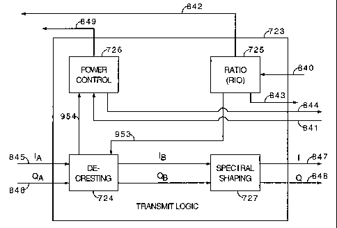
FIG. 9 depicts the transmit logic 723 from FIGS. 7-8. Transmit logic 723
includes various combinations of the following in various examples of the
invention: decresting 724, RIO 725, power control 726, and spectral shaping
727.
Decresting 724 receives the quadrature signals 845 and 846, which are referred
to as Ia and Qa respectively. Decresting 724 processes the quadrature signals
Ia
and Qa to generate correction signals that correspond to signal peaks that
exceed a threshold. The correction signals are combined with the quadrature
signals Ia and Qa to eliminate or reduce the signal peaks. Decresting provides
the resulting decrested quadrature signals lb and Qb to spectral shaping 727.
Spectral shaping 727 is comprised of digital filters that attenuate the
strength of
the in-band quadrature signals Ib and Qb to provide the shaped quadrature
signals 847 and 848.
RIO 725 receives the signal 840 which is a copy of the RF CDMA signal
provided to the antenna 719 for transmission. RIO 725 processes the signal 840
to generate ratios of in-band to out-of-band signal strength. Signal strength
can
be measured in various ways with examples being power, voltage, or energy.
RIO 725 compares the ratios to pre-determined values that represent the point
where out-of-band signal power becomes improper. RIO 725 generates a
capacity metric signal 842 and a power metric signal 843 based on the
comparison. If one of the calculated ratios exceeds its associated pre-
determined value, then the power metric signal 843 indicates that the transmit
power of the base station 722 should be limited. The capacity metric signal
842
indicates an estimate of the excess forward link capacity of the base station
722.
The estimate is typically given in a number of additional simultaneous calls
that can be handled by the base station 722 without one of the calculated
ratios
exceeding its associated pre-determined value. RIO 725 also generates a
threshold metric signal 953 based on the comparison.
Power control 726 receives the signal 841 from the power monitor 835
and the signal 954 from decresting 724. The signal 841 indicates the power of
the transmitted CDMA signal 719. The signal 954 indicates a power calculation
using the quadrature signals 845 and 846. Power control 726 compares the
CA 02364375 2001-08-23
WO 00/54428 12 PCT/US00/06227
signals 841 and 954 to generate the signals 844 and 849. The signal 844 is
provided to the gain control 833 to adjust the gain. The gain is adjusted to
maintain a pre-determined ratio of the signals 841 and 954. The signal 849 is
a
capacity control signal that indicates excess forward link capacity.
Decresting - FIGS. 10-14
Referring back to FIGS. 2 and 3, it should be noted that the Vmax voltage
levels on FIG. 2 correspond to the Pmax on FIG. 3. Thus, the peaks above
+Vmax and below and -Vmax would drive the power amplifier above Pmax
into the nonlinear operating range. When operated in the nonlinear range, the
power amplifier exhibits undesirable performance in the form of decreased
fidelity and increased noise. In addition, the CDMA base station does not meet
industry specifications, such as unused Walsh energy. Decresting eliminates or
reduces the peaks to maintain operation of the power amplifier in the
nonlinear
range, and thus improves fidelity while reducing noise.
FIG. 10 illustrates the frequency characteristics of a CDMA signal after
decresting. The vertical axis represents signal power, and the horizontal axis
represents frequency. The desired "in-band" signal power is contained within
the bandwidth defined by corner frequencies that are above and below a center
frequency. The signal power drops significantly outside of the bandwidth, but
some undesired "out-of-band" signal power is still present, and is shaded on
FIG. 10. The dashed lines above the shaded out-of-band power on FIG. 10
represent the additional out-of-band signal power generated when decresting is
not used. This additional out-of band signal power is undesirable because it
represents wasted power that interferes with other signals in neighboring
frequency bands. This reduction in out-of band signal power is typically
offset
by operating the power amplifier at a higher power level. Advantageously, the
power amplifier has greater range or capacity at the higher power level, but
does not generate intolerable out-of-band signal power.
FIG. 11 depicts representations of quadrature signals where the vertical
axis represents values for Q quadrature signals, and the horizontal axis
represents values for I quadrature signals. The time axis comes out of the
page.
The rectangular coordinate representations of the signals Qa, Qb, Ia, and lb
are
indicated on the I axis and Q axis. Radius Ra and angle 0 show a polar
coordinate representation of the quadrature signals Qa and Ia. Ra represents
CDMA signal strength and exceeds a circle labeled Rmax. Other shapes could
also be used with some examples being squares or diamonds. Rmax
corresponds to the Vmax and the Pmax of FIGS. 2 and 3 respectively. Thus, the
CA 02364375 2001-08-23
WO 00/54428 13 PCT/US00/06227
portion of Ra beyond Rmax represents a CDMA signal peak. A correction
signal Rc would reduce Ra to the Rmax circle. Rc can be represented by
quadrature correction signals Qc and Ic. Decresting is achieved by correcting
the quadrature CDMA signals Qa and la with the quadrature correction signals
Qc and Ic to generate the corrected quadrature CDMA signals Qb and lb. Since
decresting occurs in the digital domain, soft limiting is achieved that does
not
cause the undesired transients of hard limiting in the analog domain.
The threshold Rmax can be set based on various factors, such as: 1)
industry specifications for unused Walsh energy, 2) the RIO ratio of in-band
to
out-of-band signal power, 3) temperature -- lower during a cold start, 3) the
Eb/Io ratio of bit energy to interference and noise, 4) the IS-97 industry
standard Rho metric that is used to measure waveform fidelity, and/or 5) other
suitable metrics. Rmax can be adjusted during system operation based on on-
going measurements of desired metrics and corresponding adjustment of Rmax
to optimize performance.
For example, if RIO is used to control the threshold Rmax, then RIO can
be periodically measured as Rmax is incrementally increased and decreased by
a step-change. If RIO is lowered by an increased Rmax, then Rmax + delta
become the new Rmax. If RIO is lowered by a decreased Rmax, then Rmax -
delta become the new Rmax. Care should be taken to perform each of these
tests under consistent conditions
FIG. 12 depicts decresting 724. Decresting 724 receives the rectangular
quadrature signals Ia and Qa and generates the corrected quadrature signals lb
and Qb. A rectangular-to-polar conversion element 1230 receives la and Qa
and generates Ra and 0. Subtraction element 1232 subtracts Ra from Rmax to
generate Rc. Rc is negative if Ra exceeds Rmax, which occurs when a peak is
encountered. Saturation element 1234 reduces positive values of Rc to zero.
The saturation element 1234 provides Rc to the multiplication elements 1240
and 1242. The rectangular-to-polar conversion element 1230 also provides the
signal 954 indicating the quadrature signal power calculation to power control
726.
The conversion element 1230 also provides 0 to cosine element 1236 and
sine element 1238. Cosine element 1236 and sine element 1238 respectively
provide cosine 0 and sine 0 to the multiplication elements 1240 and 1242. The
multiplication elements 1240 and 1242 multiply Rc with cosine 0 and sine 0 to
respectively generate Ic and Qc. The multiplication elements 1240 and 1242
respectively provide Ic and Qc to filter elements 1244 and 1246. The filter
elements 1244 and 1246 remove out-of-band components from Ic and Qc and
CA 02364375 2001-08-23
WO 00/54428 PCT/US00/06227
14
respectively provide the signals to addition elements 1248 and 1250. The
filtering elements could also remove some in-band components as well. The
filtering is important because it converts decresting 723 from a clipping
circuit
or hard-limiter into a soft-limiter. Soft-limiting is important because it
does not
generate the unwanted transients that are produced by hard-limiting.
In addition to the conversion element 1230, Ia and Qa are respectively
provided to time delay elements 1252 and 1254. The time delay elements 1252
and 1254 introduce a time delay that corresponds to the time required to
generate Ic and Qc. The time delay elements 1252 and 1254 respectively
provide Ia and Qa to the addition elements 1248 and 1250 so that they match in
the time domain with Ic and Qc respectively. The addition element 1248 adds
Ic to ta to produce the corrected quadrature signal Ib. The addition element
1250 adds Qc to Qa to produce the corrected quadrature signal Qb.
FIG. 13 depicts an alternative version of decresting 723. Essentially, a
sampling element 1360 comprising circuitry 1362 and a low-pass filter 1364 is
added in between the saturation element 1234 and the multiplication elements
1240 and 1242 on FIG. 12. The remaining configuration and operation is
unchanged from FIG. 12.
The saturation element 1234 provides Rc to the sampling element 1360.
The circuitry 1362 samples Rc to detect a sample that exceeds the threshold
and
has the largest magnitude. This largest-magnitude sample represents a high
point in the associated CDMA signal peak. The circuitry 1362 passes only this
largest-magnitude sample that exceeds the threshold through the low-pass
filter 1364. The sampling element 1360 provides the resulting Rc to the
multiplication elements 1240 and 1242. The multiplication elements 1240 and
1242 multiply Rc with cosine 0 and sine 0 to respectively generate Ic and Qc.
Ic
and Qc are scaled versions of the negative impulse response of the lowpass
filter 1364 in sampling element 1360. The scaling is such that the negative
impulse responses, when added to the delayed signals la and Qa, will reduce
the CDMA signal peak from Ra to Rmax.
CA 02364375 2001-08-23
WO 00/54428 15 PCT/US00/06227
FIG. 14 depicts another alternative version of decresting 723. Essentially,
the quadrature logic 1470 replaces the elements 1230-1242 on FIG. 12. On FIG.
14, the decresting 723 receives the rectangular quadrature signals Ia and Qa
and
generates the corrected quadrature signals Ib and Qb. Quadrature logic 1470
processes Ia, Qa, and Rmax to produce Ic and Rc according to the following
equations:
Ic = Ia Rmax -1 and positive bracketed terms are set to zero.
Iaz +Qa2
Qc = Qa Rmax -1 and positive bracketed terms are set to zero.
Ia2 +Qa2
The quadrature logic 1470 provides Ic and Qc to filter elements 1244 and
1246 respectively. The filter elements 1244 and 1246 remove out-of-band
components from Ic and Qc and respectively provide the signals to addition
elements 1248 and 1250. The quadrature logic 1470 also generates and provides
the signal 954 which represents R2 = Iz + Q2.
In addition to the quadrature logic 1470, Ia and Qa are respectively
provided to time delay elements 1252 and 1254. The time delay elements 1252
and 1254 introduce a time delay that corresponds to the time required to
generate Ic and Qc. The time delay elements 1252 and 1254 respectively
provide Ia and Qa to the addition elements 1248 and 1250 so that they match in
the time domain with Ic and Qc respectively. The addition element 1248 adds
Ic to Ia to produce the corrected in-phase signal lb. The addition element
1250
adds Qc to Qa to produce the corrected in-phase signal Qb.
CA 02364375 2001-08-23
WO 00/54428 16 PCT/US00/06227
Spectral Shaping - FIGS. 15-16
A power amplifier is typically used to amplify CDMA signals. The
output of the power amplifier in the time domain can be mathematically
modeled as:
N
, ~ t ) = I Y n K o +J~4t)+K2i (t)+V (t) ......
n=0
where x(t) is the input to the power amplifier. If this model is transformed
from the time domain to the frequency domain, the mathematical
representation is:
Y(f) = Ko+K1X(.f)+K2(X(.f)* X(.f))+K3(X(.f)*X(.f)*X(.f))
where Y(f) is the Fourier transform of y(t) and the symbol "'F" denotes
convolution. In the context of the invention, the even terms do not contribute
significant power to the in-band signal.
Application of the well-known graphical technique for computing the
convolution of X(f) * X(f) * X(f) reveals that in-band signal power that is
input
near the corner frequencies makes a disproportionate contribution to the
unwanted out-of-band signal power that is output from the power amplifier. A
reduction of in-band signal power that is input near the corner frequencies
causes a disproportionate reduction in the unwanted out-of-band signal power
that is output by the power amplifier. The reduction of in-band signal power
does degrade the CDMA signal, but the degradation is acceptable given the
disproportionate reduction in the out-of-band signal power.
FIG. 15 illustrates the frequency spectrum of a CDMA signal that has
been amplified after being shaped by spectral shaping 727. The vertical axis
represents signal power, and the horizontal axis represents frequency. The
desired in-band signal power is contained within the bandwidth defined by
corner frequencies around a center frequency. The undesired out-of-band
signal power is shaded on FIG. 15. The dashed lines on FIG. 15 represent the
CDMA signal from FIG. 1 that was not shaped by spectral shaping 727. The
dashed lines illustrate that attenuation of the in-band signal power near the
corner frequencies produces a reduction in the undesired out-of-band signal
power.
CA 02364375 2001-08-23
WO 00/54428 17 PCTIUSOO/06227
FIG. 16 depicts characteristics of the spectral shaping 727. Those skilled
in the art recognize that FIG. 16 represents ideal characteristics, but will
recognize how to configure spectral shaping 723 based on the ideal
characteristics of FIG. 16. The vertical axis represents signal strength, and
the
horizontal axis represents frequency. The dashed lines represent the CDMA
signal before spectral shaping.
Spectral shaping 727 could be comprised of a digital or analog band-pass
filter with the following characteristics. The bandpass filter would attenuate
the signal strength in the attenuation bandwidths (ABW) by attenuation (A),
and pass the signal strength within the passband (PB). The attenuation
bandwidths ABW are adjacent to the corner frequencies and in-band, so they
are within the CDMA signal bandwidth (BW). In some embodiments, the
attenuation bandwidths (ABW) could each be 4.5% of the signal bandwidth
BW. Alternatively, the passband PB could be 91% of the signal bandwidth BW
and centered on the center frequency. The attenuation A could be 3 decibels.
Alternatively, the spectral shaping can be implemented via baseband filtering
prior to up-conversion.
An alternative version of spectral shaping 727 is described with respect
to FIG 8. Instead of placing spectral shaping 727 inside of transmit logic
723,
spectral shaping 727 is placed in the D/A converter and filter 831 in between
the D/A converter and the filter components. Spectral shaping 727 would then
be comprised of analog filters that attenuate the strength of the in-band
quadrature signals I and Q near the corner frequencies as depicted in FIG. 16.
Spectral shaping 727 would then provide the shaped I and Q signals to the
filter
components of the D/A converter and filter 631. It may be desirable in this
version of the invention to integrate spectral shaping 727 and these filter
components into a single analog filter component combining the characteristics
of the two.
RIO Control - FIGS. 17-19
FIG. 17 depicts RIO 725. RIO 725 is comprised of down-converter 1772,
transform logic 1773, and control logic 1774. The down-converter 1772 receives
the signal 840 which is a copy of the transmitted CDMA signal. The down-
converter 1772 de-modulates the RF signal 840 to form a baseband CDMA
signal 1775. The down-converter 1772 provides the baseband CDMA signal
1775 to the transform logic 1773.
FIG. 18 illustrates the frequency spectrum of the baseband CDMA signal
1775 received by the transform logic 1773. Those skilled in the art recognize
CA 02364375 2001-08-23
WO 00/54428 18 PCT/US00/06227
that FIG. 18 is an ideal representation of the signal. The vertical axis
represents
signal power, and the horizontal axis represents frequency. The desired in-
band signal power is contained within the bandwidth defined by corner
frequencies around a center frequency. Bandwidth segments 1881-1887 are
shown. Bandwidth segment 1881 is in-band, and bandwidth segments 1882-
1887 are out-of-band. The power in each bandwidth segment 1881-1887 is
shaded on FIG 18. The segments depicted on FIG. 18 are shown for illustrative
purposes, and the actual segments used could vary in number or bandwidth.
The segments could also be determined based on industry standards
The transform logic 1773 performs Fast-Fourier transforms to generate
values representing the power in each bandwidth segment 1881-1887. Those
skilled in the art are familiar with the logic required to perform such Fast-
Fourier transforms. The transform logic 1773 then generates ratio values that
will depend on the segments used. In this example, the following ratio values
are generated:
ratio 1 - bandwidth segment 1881 power/bandwidth segment 1882 power;
ratio 2- bandwidth segment 1881 power/bandwidth segment 1883 power;
ratio 3 - bandwidth segment 1881 power/bandwidth segment 1884 power;
ratio 4- bandwidth segment 1881 power/bandwidth segment 1885 power;
ratio 5 - bandwidth segment 1881 power/bandwidth segment 1886 power;
ratio 6- bandwidth segment 1881 power/bandwidth segment 1887 power.
The transform logic 1773 generates a ratio signal 1776 that indicates the
ratio values and transfers the ratio signal 1776 to the control logic 1774.
The
control logic 1774 compares each of the ratio values to an associated pre-
determined maximum value for the particular ratio. The control logic 1774
determines if any of the calculated ratios exceed their respective maximum
values.
FIG. 19 depicts a logical table containing the ratio values 1-6, the
respective maximum values, an indication if the ratios exceed the maximum
values, and the difference between the ratios and the maximum values. Those
skilled in the art are aware that the table is a logical representation that
is
capable of numerous implementations using conventional technology. The
letters A-G that are listed in the table for the power ratio entries represent
actual power measurements. The letters H-M that are listed in the table for
the
maximum value entries represent actual maximum values that can be readily
obtained in standard industry publications, such as IS-97 by the
CA 02364375 2007-08-28
74769-412
19
Telecommunication Industry Association. The Federal Communications
Commission also publishes maximum ratio values.
The control logic 1774 generates the power metric signal 843 and
transfers it to the gain control 833. The power metric signal 843 sets a flag
in
the gain control 833 if one of the ratios exceeds its maximum value. The flag
causes the gain control 833 to limit the transmit power of the base station
722.
The power metric signal 843 clears the flag when none of the ratios exceed
their
maximum values. In this fashion, the transmit power of the base station 722 is
optimized to the point set by the maximum ratio values.
The control logic 1774 generates a capacity metric signal 842 and
transfers it to a base station control system (not shown). The capacity metric
signal 842 indicates an estimate of the excess forward link capacity of the
base
station 722. To generate the estimate, the control logic 1774 determines the
average difference between the measured ratios and the maximum values and
translates the difference into a number of additional simultaneous calls that
the
base station 722 can handle without one of the calculated ratios exceeding its
associated pre-determined value. The base station control system can
determine whether or not to block call hand-offs or new calls based on the
capacity metric signal 842. In this fashion, the number of simultaneous calls
handled by the base station 722 is optimized to the point set by the maximum
ratio values.
The control logic 1774 also generates threshold metric signal 953 and
transfers it to decresting 724. The threshold metric signal sets the threshold
used by decresting 724. The use of the ratio to control power amplifier pre-
distortion is described in "Predistortion Technique For High Power
Amplifiers",
filed on June 26, 1998.
Power Control - FIGS. 20-21
FIG. 20 depicts the power control 726. Power control 726 includes: ratio
block 2090 and control block 2092. The ratio block 2090 receives signal 954
from
decresting 724. The signal 954 provides the value R2 = I2 + Q2. The ratio
block
2090 also receives the signal 841 from the power monitor 835. The signal 841
provides the value Pout which is the transmit power of the CDMA signal 719.
The ratio block 2090 determines a ratio that equals R'/ Pout. The ratio block
2090 provides the ratio in a signa12091 to the control block 2092.
The control block 2092 compares the ratio to a pre-determined value.
Those skilled in the art are familiar with how to determine this pre-
determined
CA 02364375 2001-08-23
WO 00/54428 20 PCT/US00/06227
value by considering such factors as cell size, maximum rated power, minimum
pilot signal strength at receiver, saturation, quantization errors, Ec/Io
required
at mobile device, and dynamic range of signal path. The control block 2092
generates the power control signal 844 to cause the gain control 833 to adjust
the gain of the CDMA signal. The control block 2092 configures the power
control signal 844 so the ratio moves closer to the pre-determined value. The
control block 2092 also generates the capacity control signal 849 to indicate
an
estimate of the excess forward link capacity of the base station 722. The
estimate is typically given in a number of additional simultaneous calls that
can
be handled by the base station 722. The control block 2092 transfers the
capacity control signal 849 to a base station control system (not shown).
FIG. 21 shows the desired relationship between Pout and the I2 + Q2
value. The points X and Y represent operational measurements, and the arrows
represent the control applied through the control signal 844 to the gain
control
833 to move the ratio closer to the pre-determined value. Those skilled in the
art are aware that the slope of the pre-determined value blossoms during start-
up and wilts during shut-down. Based on this document, those skilled in the
art will appreciate how to assemble the power control 726 using conventional
circuitry and software.
The previous description of the preferred embodiments is provided to
enable any person skilled in the art to make or use the present invention. The
various modifications to these embodiments will be readily apparent to those
skilled in the art, and the generic principles defined herein may be applied
to
other embodiments without the use of the inventive faculty. Thus, the present
invention is not intended to be limited to the embodiments shown herein but is
to be accorded the widest scope consistent with the principles and novel
features disclosed herein.
WE CLAIM: