Note: Descriptions are shown in the official language in which they were submitted.
CA 02364506 2001-12-07
1/18
Specification for Invention: "Integrated Timing Systems and Circuits"
by John W. Bogdan
Integrated Timing Systems and Circuits
BACKGROUND OF THE INVENTION
Field of the Invention
This invention is directed to generation of a synchronization clock for a
telecommunication system and more particularly to Integrated Timing Systems
and
Circuits (ITSC) which are used to implement universal transmission
synchronizer
(UTS).
The ITSC allow the UTS to integrate all digital PLL (DPLL) , analog PLL (APLL)
and system timing control circuits into a single ASIC solution.
The UTS may be used for wireless, optical , or wireline transmission systems
and for
a wide range of data rates.
Background Art
Maintaining accurate timing is critical to the transmission of high speed data
via
telecommunication networks. Land based, cellular, and satcom networks require
precision timing to prevent corruption of the transmitted data.
Timing is derived from external timing devices which are synchronized to a
Primary
Reference source such as a Cesium Beam Standard. (The element Cesium is
extremely stable and can be excited by radio energy to produce a 9.44GHz
reference
frequency that is electronically maintained to 1 part in 10E 13 stability).
The Global Positioning System receives and rebroadcasts a Cesium reference for
use
by telecommunication systems throughout the world. This same GPS timing signal
is
used by telecommunication systems or navigation systems.
This primary reference is not always possible. When it is not, alternate
sources are
used to maintain the performance of the appropriate telecommunication system
or
navigation system. Some kind of synchronizer is usually used to provide a
reference
clock to telecommunication equipment. Such synchronizer accepts a primary
reference source as one of its inputs. It also accepts a line input such as an
optical
transmission line.
The synchronizer passes the primary reference source to the network equipment
in
accordance to a set of performance rules. If the rules are violated, the
synchronizer
switches to the Line timing source and passes that to the network equipment.
The line
timing source is generated by a different piece of network equipment which is
also
synchronized to an external primary reference and therefore should be as
accurate as
the external input.
CA 02364506 2001-12-07
2/18
The synchronizer has its own clock which is normally synchronized to the
External or
Line input. The synchronizer clock stores information from the synchronization
reference clock.
If the synchronization reference is inten-upted, then the synchronizer uses
its stored
data to maintain the stability of its clock. This is referred as hold-over
mode. Once the
reference signal is restored the synchronizer will switch back to the
reference clock.
If the hold-over clock can not provide the stability required because the
stored data is
corrupted or some other malfunction, then the synchronizer will switch to free-
run
mode.
In free-run the accuracy of the timing signal is the basic accuracy of the
clock in the
synchronizer with no synchronization reference clock.
Current synchronizers use DPLLs for synchronized clock generation. DPLLs allow
lowering loop bandwidth in order to comply with the communication standards.
Synchronizer DPLL can be implemented using digital to analog converter (DAC),
or
direct digital frequency synthesis (DDFS), or direct digital phase synthesis
(DDPS).
Current DPLLs typically use microcomputers, EEPROM (electrically erasable
programmable read-only memory ) and a high resolution DAC (digital phase
detector) for controlling the VCXO.
Generally, the use of currently available DACs in DPLL designs necessitates
the use
of a TCVCXO (temperature compensated voltage controlled crystal oscillator).
This
special type of oscillator is expensive and must be manufactured with a
relatively
high frequency of oscillation for providing a telecommunication terminal with
a wide
range of clock signals derived from the output without having to use
additional PLLs.
However, this high frequency design makes the oscillator more expensive.
The temperature drift is yet another handicap of DAC-based designs that must
be
compensated . Also, current DAC phase drift which, as a result, may build up.
These
limitations demand additional and expensive circuitry for improving the
performance
of the DPLL.
Other known type of DPLL uses the DDFS method.
The DDFS implies eliminating each n-th pulse in an M-pulses sequence of an
incoming digital signal, filtering the resultant signal, eliminating the
undesired side
bands, and extracting the desired frequency. The circuits based on DDFS are
provided
with a microcontroller and an EEPROM for determining n, M and effecting the
deletion. Also, the DDFS algorithm requires complex logic and long acquisition
times. Furthermore, if a low frequency off shelf oscillator such as for
example a
temperature compensated crystal oscillator (TCXO) is used in this
configuration, an
additional analog PLL is necessary for obtaining the desired high frequency by
multiplying the frequency of TCXO's fixed reference clock.
CA 02364506 2001-12-07
3/18
Yet another disadvantage of the current DDFS is that the clock has rather high
jitters,
such that another additional analog PLI, is generally used for reducing the
jitters.
Still other DPLL implementation can be based on the DDPS method which has been
introduced in the US patent 5,910,753 Bogdan 08 June 1999.
Although DDPS method eliminates the above disadvantages of the DAC and DDFS
based solutions and significantly reduces complexity and cost, it still
requires external
analog amplifiers and VCXO for complete implementation of a transmission
synchronizer.
There was a need for a synchronizer and a method of synchronization which will
further reduce cost and complexity and allow higher degree of on-chip
integration by
eliminating the external analog amplifiers and VCXO for a wide variety of
telecommunication terminals.
SUMMARY OF THE INVENTION
Purpose of the invention
It is an object of present invention to provide a universal synchronizer for
use in
variety of telecommunication systems based on digital phase frequency
synthesis
(DPFS). The synchronizer of the invention may be used for wireless, optical,
or
wireline transmission systems and works well with a wide ranges of data rates.
The
synchronizer according to the invention may be used for example for SONET line-
timing (frame ) clock generation , and may be adapted to provide SONET minimum
clock (SMC) hold-over and free-run capabilities, as well as external timing
clocks
generation with Stratum 3 hold-over and free-run capabilities.
It is other object of the present invention to create systems and circuits
which allow a
complete on-chip integration by eliminating all the external components like
DACs,
VCXOs, analog PLLs, microcontrollers and EEPROMs.
Still other object of the invention is to create new digital phase detection
techniques,
which simplify currently known phase detectors logic and control algorithms of
output clock phase, while maintaining performances of leading known solutions
like
the DDPS.
CA 02364506 2001-12-07
4/18
DPFS method
Accordingly the invention provides DPFS (see FIG. 1) as a new timing method
for
programming and controlling a phase and a frequency of a synthesized clock.
The DPFS method allows programmable phase modifications which are defined
below:
phase increases of the synthesized clock are provided by adding a single gate
delay or
multiple gate delays to a present delay obtained from a propagation circuit of
a
reference clock;
phase decreases of the synthesized clock are provided by removing a single
gate delay
or multiple gate delays from a present delay obtained from the reference
propagation
circuit.
The DPFS method produces similar waveforms as commonly used DDFS method,
but DPFS inserts single gates delays into pulses stream instead of eliminating
the
whole clock cycles from a synthesized clock. Therefore, the phase hits and
resulting
fitter are reduced by 10 times compared to the DDFS method.
The DPFS method allows producing any f clock waveform by using phase steps
which are in a range of a gate propagation delay. The gate delays insertions
and
resulting phase/frequency adjustments can performed by a synthesized clock
generator (SCG) which is introduced in FIG.2A .
Synthesized clock generator (SCG)
The invention also includes the synthesized clock generator (SCG), for
carrying out
the DPFS method to produce the waveforms which are shown in FIG.l .
The SCG invention comprises 3 different SCG implementation methods, which are
explained below.
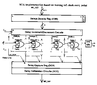
The first SCG implementation method is based on moving reference clock entry
point; wherein:
said phase increases are provided by moving an entry point of the reference
clock into
the reference propagation circuit, in a way which adds gate delays to a
present delay
obtained from the reference propagation circuit;
said phase decreases are provided by moving an entry point of the reference
clock
into the reference propagation circuit, in a way which subtracts gate delays
from a
present delay obtained from the reference propagation circuit.
The first SCG implementation method is conceptually presented in FIG.2A, and
its
principles of operations are explained below.
The delays density register (DDR) defines a number of f 3 cycles which occur
between consecutive increments or decrements of a phase of f 3 clock by a
single gate
delay time Td .
CA 02364506 2001-12-07
5/18
The delays capture register (DCR) allows capturing a waveform which contains
whole f 3 cycle. The delay calibration circuits (DCC) allow an estimation of
an
average Ta , and provide measurements of the captured f ; positioning along
the delay
line.
Based on the f 3 positioning measurements, it shall be detected periodically
that total
delay line propagation time amounts to TTOT~ Td, + T~ + ... + TdN T~~~ of f ;.
In such
cases amount of active delay elements is scaled down without changing the
phase of
the f , clock, by jumping an entry point of f 3 closer to the end of the delay
line by a
number of delay elements which corresponds to a period of the f ; clock.
The second SCG implementation method is based on moving an exit point of the
synthesized clock from the reference propagation circuit; in a way which adds
gate
delays for phase increases, and subtracts gate delays for phase decreases.
The second SCG implementation method is conceptually presented in FIG.2B, and
a
way of carrying it out is explained below:
Chain of inverters from Inv( 1 ) to Inv(N) which exists in the PLLxR frequency
multiplier, can be utilized as the reference clock propagation circuit from
which the
synthesized clock f , can be selected as having gate delays added for phase
increases
or gate delays subtracted for phase decreases. The synthesized clock selection
is
performed by a currently active output of the delay number register (DNR(1:N))
which belongs to the delay incrementldecrement circuit. As it is shown in the
FIG.2B;
any increase of DNR bit number by 1 adds 2 inverter delays to an actual phase
of the
f , clock, and any decrease of DNR bit number by 1 subtracts 2 inverter delays
from
an actual phase of the f , clock.
Said synthesized clock selection can be implemented in two different ways:
by using phase selecting gates from Sel(1) to Sel(N), as having 3state outputs
with
enable inputs EN enabled by the data number register outputs from DNR( 1 ) to
DNR(N) (see FIG.2B);
or by using NAND gates having all their outputs connected into a common
collector
configuration (instead of the 3state gates), in order to allow a currently
active DNR
output to select a phase of the synthesized clock f , .
The third SCG implementation method is based on adjusting alignment between an
exit point of the synthesized clock from the reference propagation circuit
versus an
input reference clock; in a way which adds gate delays for phase increases,
and
subtracts gate delays for phase decreases.
The third method is presented in FIG.2C, and its differences versus the FIG.2B
are
explained below.
The moving exit point from the driven by f 2 phase locked delay line is used
as a
return clock for the PLL x R multiplier, instead of using fixed output of the
Inv((N-
1 )/2+1 ) to be the PLL return clock.
The fixed output of the Inv((N-1 )/2+1 ) provides the synthesized clock f , ,
instead of
the moving reference clock exit point.
CA 02364506 2001-12-07
~~1
The exit point alignments introduce phase jumps which cause synthesized clock
fitter.
The configuration shown in Fig.2C filters out fitter frequencies which are
higher than
a bandwidth of the multiplier's PLL.
While any of the three SCG implementation methods is shown above using a
particular type of a reference clock propagation circuit, the SCG invention
comprises
using all the listed below reference clock propagation circuits by any of the
three SCG
methods:
an open ended delay line built with serially connected logical gates or other
delay
elements;
a ring oscillator built with serially connected logical gates or other delay
elements,
which have propagation delays controlled in a PLL configuration;
a delay line built with serially connected logical gates or other delay
elements, which
have propagation delays controlled in a Delay Locked Loop (DLL) configuration.
Di~italphase detector
The invention also includes a new concept of a digital phase detector DPD1
which is
shown in FIG.3. Whole UTS uses two DPDs: DPD 1 and DPD2, in a configuration
which is shown in FIG.4. Since the DPD1 and DPD2 are identical, the FIG.3
shows
DPD 1 connectivity only.
The DPD1 uses two symmetrical phase counters buffers A/B (PCBA/PCBB), which
perform reverse functions during alternative A/B cycles of the frame clock
frs2 which
is derived from the synchronized clock f Z. During the A cycle, the PCBA
counts the
number of incoming f ; clocks, but during the following B cycle the PCBA
remains
frozen until its content is read by the MC and subsequently the PCBA is reset
before
the beginning of the next A cycle. Alternatively, the PCBB performs counting
during
the B cycle and is read and reset during the following A cycle.
Such symmetrical PCBA/PCBB configuration allows much more time for counters
propagation by inhibiting counting long before the actual reading takes place.
Therefore, much higher frequencies of counted clocks are allowed for the same
IC
technology.
The above new concept of a digital phase detector, represents one of several
possible
DPD solutions; which are based on counting a first signal clock during every
second
signal frame, wherein the second signal frame contains a fixed number of the
second
signal clocks.
For all said DPD solutions, the invention further includes improving a DPD
resolution by introducing a phase capture register. The phase capture register
captures
a state of outputs of multiple serially connected gates which the first signal
clock is
continuously propagated through, at the leading edge of the second signal
frame.
Such resolution improvement is implemented in the DPD1, by using the phase
CA 02364506 2001-12-07
7/18
capture register (PCR) to measure positioning of a last fr52 edge versus f ~
waveform.
The PCR and its frame edge decoder (FED), significantly improve phase
detection
resolution.
Said improvement of a DPD resolution further comprises two different solutions
for
obtaining the first clock propagation functionality:
adding the first clock propagation circuit specifically for providing input
for the phase
capture register; or utilizing a first clock propagation circuit which already
inherently
exists in a synchronization system.
The first mentioned solution is shown in the FIG.3.
The second mentioned solution can be implemented as it is explained below.
Instead of using the added propagation circuits (APC) from the FIG.3; already
existing in the system chain of inverters Inv(1) to Inv(N) from the FIG.2B,
can be
utilized to measure the positioning of the last fr52 edge versus f 3 waveform
by
capturing the outputs of all the inverters Inv( 1 ) to Inv(N) in the phase
capture register
(PCR).
The second solution allows using shown in FIG.2B single PLLxR for producing
both
the f ; and the f ~ clocks, instead of using separate PLLxL and PLLxR as they
are
shown in FIG.4A.
The second solution eliminates any need for delay calibration of the added
propagation circuits (APC), because the replacing inverters Inv( 1 ) to Inv(N)
have
their delays controlled very accurately by the VCO Control Voltage.
Integrated synchronizer
The invention further includes a synchronizer which is completely integrated
into a
single chip (see also FIG.4A, FIG.4B, FIG.S). The integrated synchronizer
comprises;
a digital phase locked loop (DPLL) for locking an output clock to an incoming
first
reference signal, and an analog phase locked loop (APLL) for producing the
output
clock which can be locked to the first reference or to a second reference
signal.
A first/second set of reference signals is named FR~ / F~ and their single
representatives are named f ~ / f 2 accordingly, throughout this document.
The synchronizer invention further comprises three different configurations
which are
explained below.
The first synchronizer configuration is based on the SCG which does not have
an
internal frequency multiplier(see Fig.4A), and comprises circuits and
functions which
are listed below:
a synthesized clock generator (SCG) for generating a synthesized clock locked
to a
phase of the first reference signal;
a first digital phase detector (DPD 1 ) for comparing a phase of the
synthesized clock
CA 02364506 2001-12-07
~~1~
from said synthesized clock generator with a phase of a fixed reference clock,
for
producing a first phase error;
a second digital phase detector (DPD2) for comparing a phase of the first
reference
signal with the phase of the fixed reference clock , for producing a second
phase
error;
a microcontroller for driving said synthesized clock generator, based on the
first
phase error and the second phase error and in accordance with a preprogrammed
phase transfer function (PTF);
the analog phase lock loop (APLL) for generating said synchronizer output
clock;
a programmable reference selector (RFS) for said APLL, for providing reference
switching which allows the APLL to be driven by said synthesized clock or by
one of
multiple second reference signals FRZ ;
a programmable return clock selector (RTS) for said APLL, which allows
implementing different synchronization schemes;
programmable frequency dividers for reference signals (RFD) and for return
signals
(RTD) of said APLL, for providing programmable bandwidth adjustments of the
APLL;
a programmable DPLL reference selector (DRS) for selecting one of the multiple
available reference signals FR~ for said DPLL, which allows switching between
using
different DPLL reference clocks;
programmable frequency dividers in the output clock generator (OCG) which can
be
reprogrammed by the MC, in order to allow utilizing a single pin of FoUT for
providing
multiple different output clock frequencies;
activity monitoring circuits for synchronizer input clocks and output clocks;
frequency monitoring circuits for synchronizer reference clocks;
status control circuits for switching synchronizer modes of operation and
active
reference clocks, based on analysis of said activity and frequency monitoring
circuits;
phase transfer control circuits for providing required phase transfer function
between
an active reference clock and synchronizer output clocks;
a serial interface which allows the status control circuits and the phase
transfer control
circuits to be monitored and reprogrammed by an external controller;
a parallel interface which allows the status control circuits and the phase
transfer
control circuits to be monitored and reprogrammed by an external controller;
automatic reference switching functions including hold-over and free-run
switching,
which are performed by the status control circuits and are based on monitoring
a
status of the activity and frequency monitoring circuits;
a master/slave switching circuit which allows a pair of integrated
synchronizers to
work in a master/slave configuration having a slave synchronizer being phase
locked
to a mate clock which is generated by a mate master synchronizer.
a re-timing circuit in the OCG which adjusts all the rising edges of the
output clocks
FOUT of said slave synchronizer with the rising edge of the frame signal fr~TE
from said
mate master synchronizer.
The above listed status control circuits and phase transfer control circuits
can be
implemented as separate on-chip microcontrollers or with a single on-chip
CA 02364506 2001-12-07
9/18
microcontroller (MC).
The first synchronizer configuration is carried out by an UTS configuration
which is
based on the DPFS, the SCG, the DPD1 and the DPD2.
As it is shown in FIG.4A, the first configuration allows the complete
integration of
the DPLL, the APLL, and all the other circuits and functions of the integrated
synchronizer; into a single CMOS ASIC.
The on-chip implementation of a DPLL mode is explained below.
The DPD1 measures a phase error between TCXO's frequency multiplication f 3
and
synthesized clock derivative frs2 , and the DPD2 measures a phase error
between the
f 3 and the DPLL reference derivative frR~.
The MC reads the above phase errors and uses them to calculate a new contents
of
SCG's delay density register (DDR), which shall fulfill a phase transfer
function
(PTF) which is preprogrammed on the MC input.
When UTS is working in the DPLL mode, the synthesized output clock f 2 is
further
applied as a reference for the on-chip APLL which is implemented with the
programmable reference selector (RFS) and reference divider (RFD), output PLL
(OUTPLL), output clock generator (OCG), programmable return selector (RTS) and
return divider (RTD).
The on-chip implementation of an APLL mode uses an alternative reference clock
f
as a reference for otherwise unchanged the above explained APLL; by selecting
the f
on the RFS input, instead of the f z derivative of the SCG's output which
would be
selected for the DPLL mode.
It shall be noticed that the first synchronizer configuration uses lower
frequency
TCXO in order to reduce cost, and uses on-chip PLL cells to multiply TCXOs f
clock to a highest frequency which can be still feasible for a particular
technology
(see FIG. 4A). This multiplication reduces fitter as it is explained below.
Since the time period of the f 3 clock is reduced to a few nS by TCXO
frequency
multiplications; fewer delay elements are used for f z generation and power
supply
fitter introduced by the delay elements is proportionally decreased.
The invention further includes a simplified version of the first synchronizer
configuration; which can be implemented by eliminating the first digital phase
detector (DPD 1 ), and by replacing it with calculations of the first phase
error based
on analysis of SCG control signals.
The invention of the first synchronizer configuration further includes a DPLL
integrated synchronizer, which provides DPLL functions only. The DPLL
integrated
synchronizer can be obtained from the universal integrated synchronizer by
eliminating the reference selector (RFS) and the programmable frequency
dividers for
reference and return signals of the APLL (RFD and RTD), by applying the f Z
signal
directly to the OUTPLL reference input REF.
CA 02364506 2001-12-07
10/18
As it is shown in FIG.4B, the second synchronizer configuration allows the
complete
integration of the DPLL, the APLL, and all the other circuits of the
integrated
synchronizer into a single CMOS ASIC.
The second synchronizer configuration comprises the same circuits and
functions as
the listed above for the first configuration, with the exceptions which are
specified
below.
Said second configuration uses an SCG which comprises a frequency multiplier
PLLxR for producing a base frequency for the f ~ clock.
The internal SCG PLLxR multiplier provides a frequency increase which is
sufficient
for achieving a reasonable reduction of a physical size of the SCG.
Consequently the single PLLxK frequency multiplier is sufficient to provide
the SCG
driving clock f .
Still another PLLxL frequency multiplier is used with the multiplication
factor L
which is significantly different than the above mentioned factor R, in order
to produce
the f 3 clock. The f 3 drives digital phase detectors like the DPDl and the
DPD2 ,
which represent extensive heavy loads which can introduce significant on-chip
noise.
The above explained spacing between the f 3 versus the f ~ frequency reduces
impact
of inter-modulation products.
The third synchronizer configuration is based on the return clock synthesizer
(RCS)
(see the Fig.S), and comprises the same circuits and functions as the listed
above for
the first configuration; with the exceptions which are specified below.
The RCS can be implemented in identical way as any of the above described
SCGs.
Thus the RCS name indicates change in utilization only, while all the internal
functions and circuits remain the same as in the SCG.
The third synchronizer configuration is carried out by an UTS configuration
which is
based on the DPFS, the RCS, and the DPD1 and DPD2.
As it is shown in FIGS, the third configuration allows the complete
integration of the
DPLL, the APLL, and all the other circuits of the integrated synchronizer into
a single
CMOS ASIC.
As it is further shown in FIGS, the Synthesizer Status Processor (SSP) is used
to
perform all status control functions and the Phase Transfer Processor (PTP) is
designated to provide all the phase transfer processing and DPLL control
functions.
Therefore the SSP and the PTP together represent the whole functionality of
the MC
as it has been defined above for the first and the second synchronizer
configurations.
While this part of specification refers to the third synchronizer
configuration, the
invention includes using the above MC to SSP and PTP splitting for the first
and for
the second synchronizer configurations as well.
The on-chip implementation of a DPLL mode is explained below.
CA 02364506 2001-12-07
11/18
The SSP controls the input reference selector (INPREFSEL) and the reference
divider
(REF DIV) which select and divide the TCXO's f ~~ clock, in order to provide
selected reference clock f FSEL which references the analog phase detector
(APD)
which drives the JF VCXO.
The JF VCXO provides low fitter clock f ~x. which is applied as the reference
clock
for the output PLL (OUTPLL) via the output reference selector (OUTREFSEL).
The OUTPLL output ~ U~PLL is applied as the return clock for the OUTPLL via
the
output return selector (OUTRETSEL).
The OUTPLL supplies the ~ UTPLL clock for the OUTCLKGEN and the RCS.
The OUTCLKGEN provides the required set of output clocks Four.
The RCS allows implementation of the phase synthesis process as it is
explained
below.
The RCS's output clock f ~Sis applied to 1/R divider which converts the f ~S
into a
return clock for the APD.
The DPDl measures a phase error between TCXO's frequency derivative frF~ and
the
output clock multiplication f UT~T . The DPD2 measures a phase error between
the
DPLL reference derivative frR~ and the output clock multiplication f UT~T
The phase transfer processor (PTP) reads the above phase errors and uses them
to
calculate a new contents of RCS's delay density register (DDR), which shall
fulfill a
phase transfer function (PTF) which is preprogrammed on the PTP input.
The on-chip implementation of an APLL mode (see the Fig.S) selects a
derivative of
the external clock f to be the reference clock f . The f drives all the above
R2 REFSEL REFSEL
described APD, JF VCXO, OUTPLL, RCS, OUTCLKGEN in the same configuration
as described above for the DPLL mode. However during the APLL mode, the RCS
remains frozen and never introduces any changes to a phase/frequency relation
between the f clock versus the f clock.
RCS OU7PLL
The invention includes providing slave mode implementation which replaces the
external f clock with the mate UTS output clock f A~ , in order to drive the
above
described APLL configuration. The slave mode allows maintaining phase
alignment
between active and reserve UTS units, for the purpose of avoiding phase hits
when
protection switching reverts to using clocks from the reserve UTS unit.
While this part of specification refers to the third synchronizer
configuration, the
invention includes using the above mentioned method of slave UTS phase
alignment
for the first and for the second synchronizer configurations as well.
The invention further includes a simplified version of the third synchronizer
configuration, which can eliminate the JF VCXO as it is described below.
The frequency of the f FSEL clock is multiplied by S by the reference PLL
(REFPLL),
and is selected with the output reference selector (OUTREFSEL) to provide the
reference clock for the OUTPLL.
The RCS output f ~S is selected by the output return selector (OUTRETSEL) to
provide the return clock for the OUTPLL.
CA 02364506 2001-12-07
12/18
DESCRIPTION OF THE PREFERRED EMBODIMENT
~nchronizer Configuration based on SCG.
FIG.4B shows UTS configuration according to the preferred embodiment.
The UTS configuration integrates both Digital PLL (DPLL) and Analog PLL (APLL)
into a single CMOS ASIC.
DPLL configurations are explained below.
TCXOs f ~ fixed output is multiplied by PLLxK cell and by PLLxL cell up to f 3
frequency which is used as a frequency reference by the digital phase
detectors DPD1
and the DPD2.
Programmable 1 /M divider ( 1 /M DIV) allows the same input pin of the
reference
clock f ~ to be used for a variety of applications having different
frequencies of DPLL
reference clocks . The 1/M division ratio is programmed by MC OUT contents
being
written into reference programming register (RPR).
The DPD 1 measures a phase error between the synthesized clock frsz and the f
3
clock, as 0~ 1 = ~ frs2 -~ f 3.
The DPD2 measures a phase error between a DPLL reference clock frR and the f 3
clock, as~~2 = ~ frR~-~ f 3.
Based on the measurements of 0~ 1 and ~~2, microcontroller (MC) calculates
control
codes for the delay density register (DDR) of the synthesized clock generator
(SCG),
which shall implement its preprogrammed transfer function between the
synthesized
clock and the DPLL reference clock.
While the synthesized clock f Z is selected by the reference selector (RFS)
and having
the same frequency output clock f ~, is selected by the return selector (RTS),
corresponding to them reference divider (RFD) and return divider (RTD) are set
to the
same division ratio (usually these dividers are set to 1 ) in order to drive
output PLL
(OUTPLL) and output clock generator (OCG).
For most configurations the output clocks set (fort) is sufficient to drive
all the system
timing without any additional fitter filtering.
Only for some fitter sensitive applications, the output clock f ~.", can be
used as a
reference for an external narrowband Jitter Filter PLL which is implemented
with a
bandwidth adjusting programmable filter divider (FLD), an Analog Phase
Detector
(APD) and an external fitter filter crystal oscillator JFVCXO. The FLD allows
MC to
reprogram the bandwidth of the Jitter Filter PLL for different type of
applications and
for different synchronization modes. Output of the JFVCXO is named f , and is
FILX
available to be applied to a fitter sensitive circuit of a synchronized
network element.
APLL implementations use analog portions of the above DPLL configurations, but
CA 02364506 2001-12-07
13/18
the above described synthesized clock f 2 is not used as a reference for the
output PLL
(OUTPLL).
In the APLL mode, the reference selector RFS uses an alternative reference
clock f
instead of the synthesized clock f 2, as its reference clock.
The above mentioned reference and return selectors and dividers (RFS, RTS,
RFD,
RFD), allow diversified APLL configuring for a wide variety of applications
and
synchronization modes.
The DPD3 measures a phase error between an output clock f ~Z and the f ;
clock,
as0~3 = ~ f "TZ ~ f 3.
The ~~3 measurements allow the synchronizer; to detect any " f ~.Z out of
range"
condition, and to switch from the APLL mode to a "free-run mode"
Additionally the 0~3 and the 0~ 1 measurements, allow the MC to work out
SCG/DDR control codes which provide coherence of the f z signal versus the f
~Z
signal. Therefore the invention allows switching from the APLL mode to a "hold-
over
mode" , by freezing the DDR content when activity monitor detects a failure of
a
presently used reference clock
While this part of specification refers to the second synchronizer
configuration: the
invention includes using the above mentioned circuits and methods, of
switching
from the APLL mode to the free-run or the hold-over, for the first and for the
third
synchronizer configurations as well.
Similarly as for the DPLL, APLL may be configured with or without the fitter
filter
dependent of fitter levels requirements.
SCG Block Diagram and Circuits Descrption
The above mentioned third SCG implementation is selected for the preferred
embodiment, and it is shown in the FIG.2C and explained further below.
Details of the time critical Delay Shifting Register and the Delay Number
Register are
shown in FIG.6 and detailed timing is shown in FIG.7.
SCG selects outputs of the ring oscillator, based on the inverters Inv( 1 ) to
Inv(N), to
be applied as PLL return clock fSRC.
Moving the selected output forward by 2 inverters provides delayed fSRC return
clock;
which causes the PLL to speed up the synthesized clock by the delay of the two
inverters, in order to maintain phase locking between the fF2 and the fSRc
Using the return clock fSRC instead of the synthesized clock fs,, provides
additional
filtering of high frequency jitters in the fs, by the PLL Filter.
CA 02364506 2001-12-07
14/18
Said oscillator output selection is made by a single active high output of the
delay
number register DNR(1:N).
The DNR bits are controlled by the delay flip-flops DFF( 1:N) which are loaded
from
the delay shifting register DSR(1:N) by their corresponding outputs of the
ring
oscillator Inv( 1 ) to Inv(N).
In the selector shown in the FIG.2C, three state buffers are used to build the
selector,
but other configurations using open collector NAND gates can be used as well.
In order to eliminate any kind of glitches during the selection switching of
the fsRc
clock; all the switching of a presently active DNR bit must be completed while
selected oscillator output clocks remain in a low half cycle condition.
During UTS power-up sequence, the DSR(1) bit is preset to 1 and all the other
DSR(2:N) bits are reset.
Consequently, the delay shifting register DSR(1:N) always contains a single
bit active
high, while all the other bits are reset to 0.
DSR content is usually shifted right/left for INC=1/0, by a falling edge of
the fsRa
when zero content of the delay density counter DDC(1:N) is detected by the
zero
decoder (ZERDEC).
However said DSR shifting will not occur and DSR content remains frozen, if
the
STOP signal is set active high in the DDC.
The DDC( 1:N) content is decreased by 1, by a falling edge of the fsRC; when a
non
zero content of the delay density counter DDC(1:N) is detected by the zero
decoder
(ZERDEC).
The DDC( 1:N+2) content is loaded with a content of the delay density register
(DDR( 1:N+2), by a falling edge of the fsRC; when a zero content of the delay
density
counter DDC(1:N) is detected by the zero decoder (ZERDEC).
Additionally the ZERDEC = 1 condition is signaled to the MC as the MC INT, in
order to allow more accurate phase control by MC phase transfer algorithms.
The DDR is loaded by the MC OUT content, which is determined by MC phase
transfer algorithms based on measurements provided by the digital phase
detectors.
6.2 SCG Timing Analysis
The timing analysis is based on the timing diagrams which are shown in FIG.7.
The diagrams show; the fsac / fs, phase increase / decrease for INC = 1, and
the fsRC /
fs, phase decrease / increase for INC = 0.
CA 02364506 2001-12-07
15/18
For INC = 1 and ZERDEC = 0:
The fSRC keeps subtracting 1 from the content of the delay density counter
(DDC), and
the DNR( 1 ) continues selecting the output of the Inv( 1 ) to be the source
of the fSRC .
For this stage the listed below timing requirements shall be fulfilled:
The propagation delay from fSRC falling edge to eventual ZERDEC rising edge,
must
be lesser than fSRC cycle minus DDC set-up time; where the ZERDEC propagation
delay includes ZERDEC propagation through the COIJNTER/DDR SELECTOR.
For INC = 1 and ZERDEC = 1:
When ZERDEC = 1 is reached and signals that DDC content has been reduced to
zero; the fSRC falling edge shall load a content of the delay density register
(DDR( 1:N+2)) into the DDC( 1:N+2), and the reloading of the DDC with a non
zero
content shall reset the ZERDEC signal.
Additionally, the fSRC falling edge shall shift right the delay shifting
register DSR, in
order to deactivate the DSR(1) bit and to activate the DSR(2) bit.
Consequently the
next falling edge of the Inv( 1 ) will reset the DNR( 1 ) bit and the next
falling edge of
the Inv(2) will set the DNR(2) bit.
For this stage the listed below timing requirements shall be fulfilled.
The propagation delay from the fSRC falling edge to eventual ZERDEC falling
edge,
must be lesser than the delay between the fSRC falling edge cycle minus DDC
set-up
time; where the ZERDEC propagation delay includes ZERDEC propagation through
the COUNTER/DDR SELECTOR.
The total propagation delay from the Inv( 1 ) falling edge to the fSRC falling
edge plus
from the fSRC falling edge to the DSR(1) / DSR(2) falling / rising edge; must
be lesser
than the Inv( 1 ) cycle minus DNR( 1 ) / DNR(2) set up time .
It shall be noticed that for INC=l; every DFF output is inhibited from
activating a
corresponding DNR output, for as long as the previous DFF output is still
active. Said
inhibition prevents a premature activation of the next DNR bit, before the
presently
active DNR bit is reset. However even without the inhibition, the premature
activation might happen only for extremely fast selector and DSR combined with
extremely slow oscillator inverters.
For INC = 0 and ZERDEC = 0:
The fSRC keeps subtracting 1 from the content of the delay density counter
(DDC), and
the DNR(2) continues selecting the output of the Inv(2) to be the source of
the fSRC .
For this stage the listed below timing requirements shall be fulfilled.
The propagation delay from fSRC falling edge to eventual ZERDEC rising edge;
must
be lesser than fSRC cycle minus DDC set-up time; where the ZERDEC propagation
delay includes ZERDEC propagation through the COLJNTER/DDR SELECTOR.
CA 02364506 2001-12-07
16/18
For INC = 0 and ZERDEC = 1:
When ZERDEC = 1 is reached and signals that DDC content has been reduced to
zero; the fSRC falling edge shall load a content of the delay density register
(DDR(1:N+2)) into the DDC(l :N+2), and the reloading of the DDC with a non
zero
content shall reset the ZERDEC signal.
Additionally, the fSRC falling edge shall shift left the delay shifting
register DSR, in
order to activate the DSR(1) bit and to deactivate the DSR(2) bit.
Consequently the
next falling edge of the Inv( 1 ) will set the DNR( 1 ) bit and the next
falling edge of the
Inv(2) will reset the DNR(2) bit. For this stage the listed below timing
requirements
shall be fulfilled:
The prop. delay from the fSRC falling edge to eventual ZERDEC falling edge;
must be
lesser than the delay between the fSRC falling edge cycle minus DDC set-up
time;
where the ZERDEC propagation delay includes ZERDEC propagation through the
COUNTER/DDR SELECTOR.
The total propagation delay from the Inv(2) falling edge to the fSRC falling
edge plus
from the fSRC falling edge to the DSR(2) / DSR(1) falling / rising edge, must
be lesser
than the Inv(2) falling edge to the Inv( 1 ) falling edge minus DNR(2) / DNR(
1 ) set up
time .
Digital phase detectors (DPDl/DPD2)
Since both digital phase detectors are identical, only DPD1 is described
below, based
on its presentation in FIG.8 and FIG.9.
Two major digital phase detector circuits are explained below.
A symmetrical twin pair PCBA/PCBB configuration allows higher counting speeds
by eliminating all problems related to counters propagation delays.
The PCBA/PCBB configuration allows measurements of frs2 versus f 3 phase
errors,
with a resolution of a single f 3 period.
When an frS2 rise signals the end of the current phase measurement in a
currently
active phase counter (PCBA or PCBB), counting of f ; clock is inhibited and
the
phase counter content remains frozen, until the next rise of the frsZ signal
when the
counted clock will be enabled again. The whole frs2 cycle is a very long
freeze period,
which is more than sufficient to accommodate; any kind of counter propagation,
and
the counter transfer to phase processing MC, and the counter reset. During the
freeze
period a mate phase counter is kept enabled and provides measurement of frsz
phase.
Phase Capture Register (PCR) and its control and detection enhance phase
detection
resolution to a single inverter delay (i.e. by l Otimes compared with
conventional
methods based on clock counting). This enhanced phase resolution is achieved
by
capturing f 3 propagation over inverters chain with a rising edge of frS2 in
the PCR,
CA 02364506 2001-12-07
17/18
which is later decoded and transferred to the microcontroller (MC).
More detailed operations of the PCBA/PCBB configuration for both alternatives
STOPA=1 and STOPB=1, are explained below.
When STOPA signal is active, DPD circuits perform listed below functions.
PCBB counts all rising edges of f 3 clocks.
PCBB generates SEL9 signal (when PCBB(9) goes high), which activates RD REQ
which initiates MC to read PCBA via CNTR( 15:0).
MC calculates previous frsz versus f 3 phase error, by subtracting from the
newly read
PCB, the number T of f 3 clocks which nominally should correspond to the frame
frsz
(as it is shown in the FIG.4, T = N x P).
PCBB generates SEL14 signal (when CTRB(14) goes high), which activates
RST_PCBA which initiates PCBA reset circuits after its content has been read
by
MC.
When frsz rise occurs, STOP signal is activated and inverts STOPA/STOPB
signals.
When STOPB signal is active all the above functionality is fulfilled with
reversed
roles of STOPB&PCBA versus STOPA&PCBB.
Detailed timing analysis of the enhanced phase capture circuits is shown in
FIG.9 and
is explained below.
High Clock Region (HCR) signal shall be interpreted as it is defined below.
The HCR is set to 1: if f ~ rise at frs2 = high is detected by the STOP FF,
after f fall
at frsz = high was detected by the STDI FF (see FIG.B). Therefore HCR=1
signals that
frsz rising edge occurred in or around the f ~=high halfcycle, as it is shown
in the
FIG.9.
The HCR is reset to 0: if f rise at frsZ = high is detected by the STOP FF,
before
f ~ fall at frsz = high is detected by the STDI FF (see FIG.B). Therefore
HCR=0 signals
that frsz rising edge occurred in or around the f 3 = low halfcycle; as it is
shown in the
FIG.9.
PCR decoders are used for enhancing a phase detection resolution, and they are
defined below.
Last Rise Decoder (LRD) provides a binary encoded position of f 3 rising edge,
which
has been captured at the most right location of the PCR.
Last Fall Decoder (LFD) provides a binary encoded position of f 3 falling
edge, which
has been captured at the most right location of the PCR.
Cycle Length Decoder (CLD) provides a binary encoded lengths of the f 3 wave,
which has been captured between these 2 falling or 2 rising edges of the f 3
wave
which occurred at the most right locations of the PCR.
CA 02364506 2001-12-07
18/18
MC algorithms for HCR, LRD, LFD and CLD interpretation are shown in FIG.9, and
use additional terms which are explained below.
Calculated by MC measured-phase (MEA PHA) represents an actual phase error
between frS2 versus the equivalent f ; frame; and consists of the listed below
components.
CNTR-1/CNTR/CNTR-2 is an invalidated contents of a counter value CNTR which
has been read by MC (all the invalidation algorithms are detailed in FIG.9).
LRD/CLD is a normalized value of a phase error between frsz rise versus last f
3 rise,
as it has been read by MC from the LRD and CLD decoders.
Remaining-phase (REM_PHA) is calculated based on present measurement results,
but MC stores and uses it to the correct next measurement result (all the REM
PHA
calculation algorithms are shown in FIG.9).
-T = - N x P (see FIG.4 and FIG.9); transforms a captured number of f 3 cycles
per frs2
period, into a phase error between frsZ versus the equivalent f ; based frame.
It shall be noted that in most cases a first f 3 rise which occurs after frsz
rise, will set
STOP FF=1 and freeze the previously active counter by inverting STOPA/STOPB
signals. Since the first f ~ rise will still add 1 to the previously active
counter; MC
shall subtract 1 from the counter it reads, while a newly activated mate
counter will
begin with a correct 0 value. Therefore the first component of a calculated by
MC
MEA PHA shall be CNTR-1.
When frsz rise occurs during ts~ of the STOP FF and HCR=I (see the region
"CNTR-
2" in FIG.9); the second f ; rise will set STOP=1 and freeze previously active
counter
by inverting STOPA/STOPB signals. Since the first and the second f 3 rise will
still
add 1 to the previously active counter; MC shall subtract 2 from the counter
it reads,
while a newly activated mate counter will begin with an incorrect -1 value.
Therefore
the first component of a calculated by MC MEA_PHA shall be CNTR-2, and the
first
component of a stored by MC REM PHA shall be +1.
When frs2 rise occurs during th of the STOP FF and HCR=0 (see the region
"CNTR"
in FIG.9); the last passed f 3 rise has already set STOP=1 and has already
frozen
previously active counter by inverting STOPA/STOPB signals. Since the next f 3
rise
will not add 1 to the previously active counter; MC does not need to modify
the
counter it reads, while a newly activated mate counter will begin with an
incorrect +1
value. Therefore the first component of a calculated by MC MEA_PHA shall be
CNTR, and the first component of a stored by MC REM PHA shall be -1.
While the LRD/CLD represents normalized PCR captured extension of the
CNTR(15:0) captured phase, and is added to MEA_PHA; the remaining phase error
between the frsz and the next f j rise, amounts to (CLD-LRD)/CLD and it is
added to
the REM_PHA in order to modify next measurement's MEA PHA.