Note: Descriptions are shown in the official language in which they were submitted.
CA 02364525 2001-12-05
Clock Circuit for a Microprocessor
Background
1. Field of the Invention
The present invention provides a clock circuit for microprocessors. This
invention is
particularly well-suited for use in Personal Digital Assistants, mobile
communication devices,
cellular phones, and wireless two-way email communication devices
(collectively referred to
herein as "mobile devices"). The invention may provide utility, however, in
any device that is
subjected to high levels of electromagnetic interference.
2. Descriution of the Related Art
Known clock circuits commonly include crystal oscillators that resonate at a
certain
frequency. Once the crystal oscillator begins vibrating at its resonant
frequency, the resonant
frequency is typically maintained by feeding back an in-phase signal from one
terminal of the
crystal oscillator to the other terminal of the crystal oscillator. This
allows the clock circuit to
generate a substantially constant clock speed.
Known clock circuits generally have high impedances in order to reduce power
consumption. The clock circuit's high impedance, however, makes it susceptible
to interference
from strong electromagnetic signal sources. For example, in a mobile device, a
transmission
circuit may include a power amplifier that interferes with the clock circuit
during transmission,
temporarily changing the frequency of the oscillator.
Typical mobile devices isolate the clock circuit from the strong
electromagnetic
interference that occurs during transmission by shielding the clock circuit
with an EMI shield. In
1
CA 02364525 2005-04-O1
addition, a typical mobile device may include an external buffer amplifier
that protects the
integrity of the clock circuit. These known techniques generally add
complexity and high
component counts to the device. Furthermore, the;~e techniques may require the
circuit to
restart the crystal oscillator in the event that the os~~illation has stopped
or slowed as a
result of a strong interference signal.
Summar3~
A clock circuit is disclosed which comprises an analog clock element, a
digital
clock element, and a controller. The analog clock element is configured to
generate an
oscillating output. The digital clock element is configured to generate a
digital clock
output. The controller is configured to switch bet~Neen the analog clock
element and the
digital clock element. The oscillating output and ~:he digital clock output
have
substantially equivalent frequencies.
In a first embodiment of the present invention, there is provided a clock
circuit for
a mobile device, the clock circuit having a clock circuit output, comprising a
controller
configured to receive a state signal having a first state and a second state,
wherein the state
signal is in the first state while the mobile device is transmitting and is in
the second state
while the mobile device is receiving a transmission, the controller further
configured to
generate a digital clock enabling signal when the state signal is in the first
state and to
generate an analog clock enabling signal when th~~ state signal is in the
second state; an
analog clock circuit coupled to the controller to rf;ceive the analog clock
enabling signal
and configured to generate an oscillating output, wherein the oscillating
output is enabled
as the clock circuit output when the analog clock circuit receives the analog
clock enabling
signal from the controller; and a digital clock circuit coupled to the
controller to receive
the digital clock enabling signal and configured t~ generate a digital clock
output having a
frequency that is substantially equal to the frequency of the oscillating
output,
2
CA 02364525 2001-12-05
wherein the digital clock output is enabled as the clock circuit output when
the digital clock
circuit receives the digital clock enabling signal from the controller.
According to a further aspect of the present invention, a clock circuit
comprises an analog
clock element configured to generate an oscillating output, a digital clock
element configured to
generate a digital clock output, and a controller configured to switch between
the analog clock
element and the digital clock element, wherein the oscillating output and the
digital clock output
have substantially equivalent frequencies.
In a still further embodiment of the invention, a method of isolating a
crystal oscillator in
a mobile device from electromagnetic interference comprises the steps of
receiving a state signal
which indicates that generation of an electromagnetic field near the crystal
oscillator is
anticipated, detecting an edge of a clock circuit signal after the state
signal has been received,
and enabling a digital clock circuit and disabling the crystal oscillator from
the clock circuit
when the edge is detected.
A method of maintaining oscillation of a crystal oscillator, according to
another aspect of
the invention, comprises the steps of detecting an edge of a clock circuit
signal, enabling a digital
clock circuit when the edge is detected, and driving the crystal oscillator
with the digital clock
circuit, wherein the output of the digital clock circuit and the crystal have
substantially
equivalent frequencies.
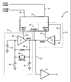
Brief Description of the Drawings
FIG. 1 is a circuit diagram of an exemplary clock circuit according to the
present
invention; and
FIG. 2 is a timing diagram related to the circuit shown in FIG. 1.
3
CA 02364525 2001-12-05
Detailed Description of the Drawings
With reference to the drawing figures, FIG. 1 is a circuit diagram of an
exemplary clock
circuit according to the present invention. The clock circuit includes a
controller 12, an analog
clock element 21, a digital clock element 23, a state signal 14 and a timing
signal 16. The state
signal 14 may, for example, be coupled to the transmission circuitry of a
mobile device and
configured to deliver a high pulse while the mobile device is transmitting.
The timing signal 16
may, for example, be generated by a frequency synthesizer in a mobile device.
The controller
12 is coupled to the timing signal 16 and the state signal 14, and generates
an analog clock
enabling signal 20 and a digital clock enabling signal 22. The analog clock
enabling signal 20 is
coupled to the analog clock element 21, and the digital clock enabling signal
22 is coupled to the
digital clock element 23. The respective output terminals of the analog and
digital clock
elements 21 and 23 are coupled together to generate the clock signal 10, which
is output to be
used by other circuits (not shown), possibly through an output buffer 11. In
addition, the clock
signal 10 is coupled as a trigger input 52 to the controller 12, and operates
to synchronize the
switching of the enabling signals 20 and 22 such that the switching operation
occurs timely to
both the period of the clock signal 10 and either a leading or falling edge of
the timing signal 16.
The relationship between the trigger input 52, the timing signal 16 and the
enabling signals 20
and 22 is discussed below in more detail with reference to FIG. 2.
Operationally, the controller 12 enables either the analog clock element 21 or
the digital
clock element 23 as a function of the state signal 14. For instance, while a
mobile device is
either idle or receiving a transmission, the state signal 14 may be in a first
state, causing the
controller 12 to enable the analog control element 21. Then, while the mobile
device is
4
CA 02364525 2001-12-05
transmitting, the state signal 14 may be in a second state, causing the
controller 12 to enable the
digital clock element 23. In this manner, the clock circuit 14 isolates the
analog clock element
21 from the electromagnetic interference that is typically generated while the
mobile device is
transmitting, and thus maintains a substantially constant clock signal 10.
The analog clock element 21 preferably includes the oscillator amplifier 26, a
resistor 36,
a crystal oscillator 40, and a plurality of capacitors 42, 44, and 46. The
crystal oscillator 40, the
oscillator amplifier 26, and the resistor 36 are coupled in parallel. The
capacitors 42 and 44 are
coupled in series between ground and the input of the oscillator amplifier 26.
The capacitor 46 is
coupled in series between the output of the oscillator amplifier 26 and
ground. The resistor 36 is
a negative feedback element that couples the output voltage of the amplifier
26 to both the input
of the crystal oscillator 40 and the amplifier 26. In addition, the resistor
36 biases the amplifier
26 such that the amplifier 26 operates in a high-gain linear region. Together,
the amplifier 26
and the capacitors 44 and 46 shift the phase of the output to maintain
oscillation. The values of
the resistor 36 and the capacitors 44 and 46 are preferably determined by the
desired gain of the
amplifier 26 and the load capacitance of the crystal oscillator 40,
respectively. In one alternative
embodiment, the analog clock circuit 21 may also include an additional
resistor between the
output of the crystal oscillator 40 and output of the resistor 36.
The digital clock element 23 includes the digital amplifier 28 coupled to a
frequency
matching output 50 from the controller 12. The frequency matching output 50 is
preferably a
square wave generated by the controller 12 that has a frequency substantially
equal to the
frequency of the analog element 21. The frequency matching output 50 may be
generated, for
example, by a divider internal to the controller 12 that counts cycles of the
timing signal 16. In
this manner, the frequency matching output 50 is generated by dividing the
frequency of the
CA 02364525 2001-12-05
timing signal 16. For instance, after a predetermined number of cycles of the
timing signal 16
have been counted, then the controller 12 can generate a pulse, change the
signal level of the
frequency matching output 50 from the low level to the high level or, if the
frequency matching
output 50 is high, from the high level to the low level. When the digital
amplifier 28 is enabled
by the digital enabling signal 22, the digital amplifier 28 generates the
clock signal 10 with a
frequency substantially equal to the frequency of the frequency matching
output 50.
Operationally, the state signal 14 determines which clock element 21 or 23
generates the
clock signal 10. When the state signal 14 is in a first state, the oscillating
amplifier 26 is
enabled, the digital amplifier 28 is disabled, and the clock signal 10 is
generated by the analog
clock element 21. When the state signal 14 changes state, the controller 12
preferably waits for a
trigger input 52 and a new cycle in the timing signal 16, and then reverses
the states of the
enabling signals 20 and 22. Once the state change has been triggered, the
digital amplifier 28 is
enabled, the oscillating amplifier 26 is disabled, and the clock signal 10 is
generated by the
digital clock element 23. In addition, the clock signal 10 from the digital
amplifier 28 is coupled
to the crystal oscillator 40 through the feedback resistor 36 to enable the
crystal oscillator 40 to
continue to oscillate while the oscillating amplifier 26 is disabled.
FIG. 2 is a timing diagram related to the circuit shown in Fig. 1. The timing
diagram
includes the state signal 14, the timing signal 16, an analog output signal 58
(xouta), a digital
output signal 60 (xoutb), and the trigger input 52. The timing diagram also
shows five dotted
lines 71, 72, 73, 74 and 75 that are included to refer to points in time when
significant signal
changes occur, and are respectively referred to hereinafter as REF 71, REF 72,
REF 73, REF 74
and REF 75.
6
CA 02364525 2001-12-05
In a left to right view of the signals, the oscillator amplifier 26 is
initially enabled,
generating an alternating high/low pulse as the analog output signal 58. The
digital amplifier 28
is initially disabled, with the digital output 60 in a high impedance state.
The trigger input 52,
which is coupled both to the analog and digital output signals 58, is
initially driven by the analog
output signal 58.
At REF 71, the state signal 14 changes states (from low to high), instructing
the
controller 12 to switch from the analog clock element 21 to the digital clock
element 23. In
order to synchronize the clock element switch with the clock output 10, the
controller 12
preferably waits for the rising edge of the clock pulse 10 at its trigger
input 52, indicating the
beginning of a new cycle in the clock output 10. This is shown in Fig. 2 at
REF 72. In addition,
because the digital output 60 is generated as a function of the timing signal
16 as described
above, the digital and analog clock elements 21 and 23 should preferably not
be switched until
the timing signal 16 starts a new cycle at REF 73. Otherwise, the clock output
10 could be
switched over to the digital clock element 23 before the controller begins
dividing the timing
signal 16 to generate the frequency matching output 50, resulting in a glitch
in the clock output
10. Thus, from REF 71 until REF 73 the clock output 10 (and trigger input 52)
is driven by the
analog output 58. This results in a short delayed pulse 80 from the analog
output 58 that occurs
before the clock elements 21 and 23 are switched at REF 73.
From REF 73 to REF 74, the digital amplifier 28 is enabled, generating an
alternating
high/low pulse as the digital output signal 60 that has a frequency
substantially equal to the
oscillation frequency of the oscillator 40. The oscillator amplifier 26 is
disabled, and its output
assumes a high impedance state. The trigger input 52 is being driven by the
digital output signal
60.
7
CA 02364525 2001-12-05
At REF 74, the state signal 14 again changes states (from high to low),
instructing the
controller 12 to switch back to the analog clock element 21. As explained
above, while the
analog clock element 21 is disabled, the oscillator 40 is driven by the
digital output signal 60 and
thus maintains synchronization with the clock output 10. Therefore, when the
controller 12
receives a state signal 14 at REF 74, instructing a switch from the digital
clock element 23 to the
analog clock element 21, the controller 12 preferably only waits for an
appropriate signal on its
trigger input 52 before initiating the switch. In a preferred embodiment, the
switch between the
digital output 60 and the analog output 58 is triggered at the falling edge of
the trigger input
signal 52 (REF 75) to avoid glitches in the clock output 10.
In one exemplary embodiment, the timing circuit 8 described above with
reference to
FIGs. 1 and 2, may be implemented in a wireless communication device. For
example, a
handheld, wireless communication device may communicate with a base station
through a
wireless modem. When the handheld device is idle or is otherwise not
communicating, the
device sends a low state signal 14 to the circuit 8. The circuit synchronizes
the microprocessor
of the device using the analog clock element 21 which preferably resonates
with a 32.768 kHz
crystal. During this time, the digital clock element 23 remains in a disabled
state and the digital
amplifier output is in a high impedance state.
When the handheld device is communicating with the base station and thus
generating a
high level of electromagnetic interference, the device sends a high state
signal 14 to the circuit 8.
The high state signal 14 alerts the controller 12 to switch between the analog
clock element 21
and the digital clock element 23. When an edge of the analog output signal 58
is sensed at the
trigger input 52, then the controller disables the analog element 21 and
enables the digital
element 23. The crystal is then protected from the high EMI fields associated
with
8
CA 02364525 2001-12-05
communication signals that may otherwise overwhelm the crystal oscillator 40
when the
handheld device is transmitting voice and/or data messages. Other
electromagnetic disturbances
may similarly be anticipated by the device to initiate a switch from the
analog clock element 21
to the digital clock element 23.
The embodiments described herein are examples of structures, systems or
methods
having elements corresponding to the elements of the invention recited in the
claims. This
written description may enable those skilled in the art to make and use
embodiments having
alternative elements that likewise correspond to the elements of the invention
recited in the
claims. The intended scope of the invention thus includes other structures,
systems or methods
that do not differ from the literal language of the claims, and further
includes other structures,
systems or methods with insubstantial differences from the literal language of
the claims.
9