Note: Descriptions are shown in the official language in which they were submitted.
CA 02364918 2001-08-21
WO 00/57680 PCT/EP00/02560
1
Method for manufacturing a multilayer printed circuit board and
composite foil for use therein
The present invention generally relates to the manufacturing of a multilayer
printed circuit board and to a composite foil for use therein.
The development of very compact and powerful electronic devices has been
possible thanks to high-density printed circuit boards (PCB), obtained by
sequential build-up (SBU) technology. Basically, a build-up multilayer circuit
is a
combination of several superimposed layers of different wiring densities,
which
are separated by dielectric layers and interconnected through micro blind vias
with diameters of generally less than 100 m.
Nowadays, essentially three different technologies are available for the manu-
facture of microvias: (1) the photochemical etching of photodielectrics; (2)
the
plasma etching process; and (3) the still relatively new process of laser
drilling.
Laser drilling seems to be the most promising technology for the production of
microvias. Excimer, Nd-YAG and CO2 laser sources are currently used for
drilling of microvias, but each of these laser sources still has its specific
draw-
backs. Excimer lasers are not considered economically viable for industrial
use.
They have a low ablation rate per pulse and involve high investments in safety
precautions, as excimer laser gases are extremely corrosive and highly toxic.
Nd-YAG lasers are successfully used for smaller and medium sized volumes of
high end products with microvias of diameters from 25 to about 75 m. Larger
holes must be produced by trepanning (i.e. by drilling multiple smaller
holes),
which of course reduces drilling speeds considerably. CO2 lasers are increas-
ingly gaining ground vis-a-vis the Nd-YAG laser for a large volume production
of
microvias. They are characterised by an ablation rate in non-reinforced
polymer
that is about twenty times as high as for Excimer or Nd-YAG lasers.
However, if CO2 lasers are very much adapted for polymer ablation, they are
not suitable for copper removal. Hence, an additional process step, the manu-
CONFIRMATION COPY
CA 02364918 2001-08-21
WO 00/57680 PCT/EP00/02560
2
facturing of a conformal mask, is necessary before a hole can be produced in
the dielectric layer with the CO2 laser. During this additional step, openings
are
etched in the copper laminate at the positions where the dielectric should be
removed later. This method allows to use the CO2 laser for drilling blind
micro-
vias, but the manufacturing process is slowed by the conformal mask building
step and there is a real risk of damaging the copper layer during the
conformal
mask building.
In order to avoid the above and other disadvantages of the conformal mask
technology, it has been suggested to use a twin laser device for drilling the
holes. Such a twin laser device is a combination of CO2 laser source with an
IR
solid-state laser. First, the opening in the copper foil is carried out with
the solid-
state laser. The resin layer is then removed with the CO2 laser. Such a twin
laser allows microvia drilling in copper cladded build-ups, but the investment
cost is higher than for a simple CO2 laser, and the slow copper drilling step
is
responsible for a low process speed.
It has also been suggested to replace the manufacture of the conformal mask
by a "half etching" step. A thin resin coated copper foil of about 18 m is
first
laminated on the core board, with its copper foil upside. After lamination,
the 18
m copper foil is etched over its entire surface, in order to reduce its
thickness
down to about 5 m. In the next step, the copper layer undergoes a black oxide
treatment, to form a laser drilling adapted surface. Then, the CO2 laser is
used
to drill the microvias directly through the 5 m copper layer and the
subjacent
resin layer. The "half etching" step is of course less complex than conformal
mask building, but the manufacturing process is nevertheless slowed down by
the half etching step and the copper surface might still be damaged during the
half etching step. Furthermore, CO2 laser drilling on "half etched" copper
foils
does not yet produce satisfying results. The poor results are due to the fact,
that
etching the entire surface of e.g. a 600 mm x 500 mm printed circuit board is
neither a homogeneous, nor a precise operation. The most recent etching
agents and etching machines claim a tolerance of 2 m. The thickness of a
copper foil etched down to a nominal thickness of 5 m may therefor vary from
= 01-06-2001 EP 000002560
CA 02364918 2001-08-21
WO 00/57680 PCT/Eroo/02560
3
3 m to 7 m. When drilling the microvias, the laser energy is set for a
nominal
copper thickness of 5 m. If the copper layer at the incidence point is only 3
m,
the set laser energy is too high for the amount of copper to be vaporised. As
a
result, copper splashes are created on the border of the hole and the hole in
the
dielectric material is generally misshaped. If the copper layer at the
incidence
point is however 7 m, the set laser energy is too low and the resulting hole
in
the dielectric material will have too small a diameter or will even not extend
to
the subjacent copper layer. Due to the disappointing results of the half
etching
method, CO2 laser drilling is still exclusively used on non-copper cladded
build-
up materials or with conformal mask etching.
US 3,998,601 discloses a composite foil and a method for manufacturing the
latter. The composite foil comprises an electrodeposited copper support layer
and a second electrodeposited copper layer of a thickness which is not self
supporting. Intermediate the copper support layer and the second copper layer
is a thin layer of a release agent, preferably chromium. The second copper
layer
has a thickness no greater than 12 m. A laminate may be formed by superim-
posing this composite foil on epoxy impregnated fiberglass with the ultrathin
copper surface in contact with the epoxy-glass substrate, and subjecting this
assembly to a conventional laminating process. After cooling of the laminate,
the copper carrier coated with the release agent is peeled away-to produce a
thin copper clad laminate suitable for etching, etc. in the production of
printed
circuit elements.
A method for manufacturing a multi-layer interconnected board is described in
JP 10 190236. According to a first step of this method , a circuit board with
a
desired circuit pattem formed thereon, a metal foil and an insulator layer are
positioned, stacked up and laminated. In the next step, a point on a conductor
layer desired to be laser processed is subjected to a process to increase the
rate of absorption of the laser. In the following step a laser beam is
impinged on
the processed point so as to melt and sublime the metal foil and the insulator
layer and thereby form a hole. In a final step, electroless plating is
performed to
electrically connect conductors through the hole.
AMENDED SHEET
01-06-9001 EP 00000256C
CA 02364918 2001-08-21
WO 00/57680 PCT/EP00/02560
The possibility of laser driiling into copper clad epoxy-glass, in particular
by
means of a C02 laser, is reported in "Laser drilling of microvias in epoxy-
glass
printed circuit boards" by A. Kestenbaum et al., IEEE Transactions on compo-
nents, hybrids and manufacturing technology, vol.13, no. 4, December 1990
(1990-12), pages 1055-1062, XP000176849 IEEE Inc. new York, US ISSN:
0148-6411. In one of the experiments, a CO2 laser was used to drill a through
hole in a 0.254 mm (10-mil) epoxy-glass layer clad with 4.4 m (1/8-oz) copper
on both sides. In another experiment a CO2 laser was used to drill a blind
hole
in a 0.254 mm (10-mil) epoxy-glass layer clad with 4.4 m (1/8-oz) copper.
DE-A-31 03 986 relates to a process for the production of drilled holes for
the
throughplating in printed circuit boards consisting of substrate materials on
the
basis of carbon. The throughholes are drilled using a C02 laser. The metal
layer on top of the printed circuit board may be coated with a radiation-
specific
acceptor to improve the absorption of the laser beam. In case the metal layer
is
made of copper, the acceptor may be made of Copper-li-oxide.
Consequently, there is a strong need for a simple and efficient method for the
manufacture of multilayer printed circuit boards, which allows fast laser
drilling
of high-quality microvias. According to the present invention, this object is
achieved by a method according to claim 1.
Another object of the present invention is to provide a composite foil, which
allows fast laser drilling of high-quality microvias, when it is used in the
manu-
facture of multilayer printed circuit boards. According to the present
invention,
this object is achieved by a composite foil according to claim 14.
In accordance with the present invention, a method for manufacturing a multi-
layer printed circuit board comprises the following steps:
a) providing a core board;
b) providing a composite foil including a functional copper foil of less than
10
m mounted on a carrier foil, said copper foil having a front side facing
said carrier foil and a back side coated with a non-reinforced thermoset-
ting resin;
AMENDED SHEET
01-064001 EP 00000256C
~ CA 02364918 2001-08-21
' WO 00/57680 PCTlEPOOro2560
3b
c) laminating said composite foil with the resin coated back side on one side
of said core board;
d) removing said carrier foil from said functional copper foil, in order to un-
cover said front side of said functional copper foil;
e) driliing holes through said functional copper foil and said resin in order
to
form microvias.
AMENDED SHEET
CA 02364918 2001-08-21
WO 00/57680 PCT/EP00/02560
4
According to an important aspect of the present invention, the functional
copper
foil of the composite foil has a thickness of less than 10 m, preferably of
about
m, whereby it becomes possible to use a CO2 laser source to drill microvias
directly from the uncovered front side through the very thin functional copper
foil
5 and the subjacent dielectric layer. It follows that "half etching" or
"conformal
mask building" steps are no longer necessary, so that the manufacturing
process of a multilayer PCB gets simpler. The simplicity of the process
enables
high speed processing and high productivity, with less process equipment and
therefore lower investment costs. In other words, the process of manufacturing
gets more efficient. Consumption of chemical etching agents is also substan-
tially reduced. This is of course an important feature with regard to environ-
mental protection. With regard to quality control, it will be noted that the
thin
functional copper foil has an accurate thickness and a controlled and homoge-
nous surface profile and roughness, so that the CO2 laser beam encounters
similar and reproducible drilling conditions everywhere. It follows that the
laser
energy can be set to drill very precise microvias everywhere on the PCB, i.e.
microvias having a well determined shape, diameter and height, without
producing copper splashes on the copper surface. It will further be
appreciated
that the carrier provides the necessary rigidity for handling the functional
resin
coated copper foil. Moreover, the latter is protected between its carrier and
its
resin coating against particles, chemical agents or atmospheric agents, that
may damage the surface integrity, and alter the future circuit pattern. Due to
the
self supporting carrier foil, not only the very thin functional copper foil,
but also
the rather brittle resin coating is protected against tears, cracks and
wrinkles.
During lamination, the carrier provides an efficient protection of the very
thin
functional copper foil against dust and particles (as e.g. resin particles),
which
may indent the surface, and against resin bleed-through. After removal of the
carrier, the functional copper layer is consequently clean and free of any
defects
such as e.g. indentations, tears, cracks and wrinkles.
The functional copper foil is preferably obtained by electro-deposition.
Advanta-
geously, the front side of the functional copper foil has received a surface
preparation favouring the absorption of CO2 laser light. Such a surface
prepara-
01-06-~5001 EP 00000256C
CA 02364918 2001-08-21
= WO 00/57680 PCT/EPOO/02560
tion may e.g. provide a front side having a particular surface profile and
rough-
ness and/or a colour favouring the absorption of CO2 laser light. It can take
place during manufacturing of the composite copper foil, so that the
functional
copper foil is ready for laser driliing after removal of its carrier. The
front side of
5 the functional copper foil may also be covered prior to laser drilling with
a black
oxide conversion coating, thus favouring the absorption of COZ laser light.
It will be noted that the composite foil preferably includes a release layer
intermediate the carrier foil and the functional copper foil. Such a release
layer
may simply permit the separation of the carrier foil, like e.g. a thin,
chromium
based release layer. In this case, the carrier removal then normally consists
in
mechanically peeling off the carrier foil and the release layer
simultaneously, i.e.
the release layer remains bonded to the carrier foil. However, another kind of
release layer may remain on the functional copper foil instead of the carrier
foil
when removing the carrier foil, and exhibit a particular surface colour
favouring
the absorption of CO2 laser light. Such a kind of release layer, having a dual
function, may be a dark coloured conductive material layer and should allow
copper electroplating to form the functional copper foil thereon, show a
strong
adhesion to the functional copper foil, and have a colour favouring the absorp-
tion of the infrared light of a CO2 laser.
In a first embodiment, the resin is a B-staged resin. It can therefore adapt
to the
subjacent circuits of the core board, and the polymerisation is completed
during
lamination.
In a second embodiment, the resin coating on the back side consists of a C-
staged resin layer applied to the back side of the functional copper foil, and
of a
B-staged resin layer applied to said C-staged resin layer. The insulating
layer is
therefore thicker and can still adapt to the subjacent circuit layer.
It will be appreciated that the present invention also provides a composite
foil
for use in a method for manufacturing a multilayer printed circuit board, corn-
prising a seff-supporting carrier foil, preferably a copper foil with a
thickness
from 18 to 150 m; a release layer on one side of the carrier foil; a
functional
copper foil, having a thickness of less than 10 m, most preferably of
AMENDED SHEET
011-06-,~001 EP 00000256C
CA 02364918 2001-08-21
. WO 00/57680 PCT/EP00/02560
6
about 5 m, the functional copper foil being deposited on the release layer
and
having a front side facing the release layer and a back side; and a non-
reinforced thermosetting resin coating on the back side of the functional
copper
foil.
The front side of the functional copper foil has preferably received a surface
preparation favouring the absorption of CO2 laser light. Such a surface
prepara-
tion may be carried out by forming a dark coloured conductive material layer
between the release layer and the functional copper foil. In a first
embodiment
of the composite copper foil of the invention, the dark coloured conductive
material layer may comprise carbon black and/or graphite. In a second em-
bodiment, the dark coloured conductive material layer may comprise a dark
coloured electrically conductive polymer layer.
It shall be noted that the release layer may itself be a dark coloured
conductive
material layer, thereby exhibiting a dual function of release layer and
surface
preparation favouring the absorption of C02 laser light. The composite foil
would then comprise a carrier foil, this release layer having a dual function,
a
functional copper foil, and a resin coating. It is clear that such a release
layer,
contrary to a conventional release layer like e.g. a chromium release layer,
has
to adhere to the front side of the functional copper foil when removing the
carrier foil.
Advantageously, the back side of the functional copper foil has a bonding
layer
thereon so as to improve its bond strength with the resin coating. Moreover,
the
functional copper foil may be covered with a passivation layer, preferably
intermediate the bonding layer and the resin coating, in order to warrant the
stability of the back side. =
The present invention will be more apparent from the following description of
a
not limiting embodiment with reference to the atfached drawings, wherein
Fig.1: is a cross-sectional S.E.M.-view of a composite foil used for the manu-
facturing of a multilayer printed circuit board; and
Fig.2: is a diagram showing the process steps of the manufacturing of a
multilayer printed circuit board.
AMENDED SHEET
CA 02364918 2001-08-21
WO 00/57680 PCT/EP00/02560
7
The present method uses a composite foil 10, more precisely a resin-coated
carrier-mounted copper foil for building a multilayer PCB. Figure 1 shows a
Scanning Electron Microscope view of such a composite foil, which will be
laminated on a core board. It comprises four different layers: a carrier foil
12; a
release layer 14; a functional copper foil 16; and a resin coating 18. Such a
composite foil is the result of two subsequent manufacturing processes.
The first process is similar to the process described in US 3,998,601. First,
a
70 m carrier foil 12 is produced from an acid based electrolyte by continuous
electro-deposition on a rotating titanium drum that has a precisely engineered
surface. The drum surface topography prescribes and controls the initial layer
of
copper deposited. The topography of the other side, the matte side, of the
carrier layer is controlled by the additives in the basic drum copper
electrolyte.
In a further step the release layer 14 is applied to one surface of the
carrier foil
12, providing very closely controlled, but relatively low adhesion
characteristics.
The release layer 14 has a very thin thickness, typically less than 1 m. The
functional copper foil 16 is electrodeposited onto the release layer 14 with a
thickness of preferably 5 m. The side of the functional copper foil 16 facing
the
carrier foil 12, called hereinafter the front side, is consequently a mirror
image of
the surface of the carrier foil 12 which is covered with the release layer 14.
It
follows that acting on the structure of the surface of the carrier foil 12
which is
covered with the release layer 14 enables to provide a particular surface
profile
and roughness to said front side of the functional copper foil 16. The other
side
of the functional copper foil 16, hereinafter called the back side, is a matte
side.
This back side undergoes a series of chemical and electrochemical treatments,
that will define some functional characteristics, such as bond strength with
regard to the resin coating and stability with regard to corrosion. Hence a
bonding layer, obtained by electrodeposition of copper nodules, is formed on
the back side of the functional copper. Then a passivation layer is applied
over
the bonding layer. It may be noted that a passivation layer may also be
applied
over the exposed side of the carrier foil 12, i.e. not bearing the release
layer 14,
in order to avoid the formation of a "blue oxidation frame" during PCB manu-
facturing, e.g. in a press.
CA 02364918 2001-08-21
WO 00/57680 PCT/EP00/02560
8
In the following process, the composite copper foil 12, 14, 16 is processed in
a
coating machine, where the back side of the functional copper foil 16, already
covered by the bonding layer and the passivation layer (not shown on the
Figures), is coated with a non-reinforced thermosetting preferably semi-
polymerised (B-staged or semi-cured) resin. The use of a B-staged resin is
very
convenient when the composite foil is laminated on a core board. Indeed, since
the resin is only semi-polymerised, it can adapt to the subjacent topography
of
the outer layer circuits of the core board. On top of that, the polymerisation
of
the B-staged resin can be finished (leading to C-staged resin) during
lamination
since it is e.g. carried out in a hydraulic press or in an autoclave with
heating
and cooling cycles.
The resinous coating 18 may also comprise two superimposed layers. One first
thin layer (25-45 m) of C-staged resin is applied on the functional copper
layer,
and a second layer of semi-cured resin is applied over the precedent one. This
way of processing achieves a thick resinous coating and is much easier and
safer than applying a single layer of B-staged resin having the same
thickness.
It is of course also possible to apply more than two resin layers in order to
reach
the desired thickness.
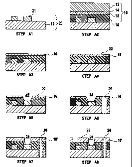
Figure 2 illustrates a preferred manufacturing process of a multilayer printed
circuit board in accordance with the present invention.
The process starts in step Al with the provision of a finished core board 20.
The
core board 20 shown in Fig. 2 consists e.g. of a one-sided copper-cladded
prepreg 19, where circuit patterns 21 have already been etched into the copper
clad. The circuit patterns 21 are preferably surface treated by oxidation or
roughening, in order to achieve a higher bonding strength with the subsequent
overlying dielectric material.
In step A2, a composite foil 10, obtained as described hereinbefore, is lami-
nated on one side of the core board 20, wherein the resin coating 18 of the
composite foil 10 faces the circuit patterns 21 on the core board 20. This
lamination takes place in a hydraulic press and involves preferably several
cooling and heating cycles. During the lamination step, the polymerisation of
the
CA 02364918 2001-08-21
WO 00/57680 PCT/EP00/02560
9
B-staged thermosetting resin is completed. It shall be remarked that a greater
dielectric thickness can be obtained by placing an interlaminar dielectric
sheet
between the core board 20 and the composite foil 10 before lamination.
Once the lamination is finished and the resin 18 is fully polymerised, step A3
takes place, i.e. the carrier foil 12 and the release layer 14 are
mechanically
peeled off. The very thin release layer 14 remains bonded to the 70 m copper
carrier foil 12, leaving an atomically clean, homogeneous and defect free
functional copper layer 16 on top of the core board 20.
In step A4, the functional copper foil 16 preferably undergoes a surface treat-
ment, in order to prepare its front side for direct CO2 laser drilling. This
surface
treatment may consist in the deposition of a black oxide conversion coating 22
on the functional copper foil 16. The black oxide conversion coating warrants
indeed an efficient CO2 laser drilling, because it reduces laser light
reflection on
the uncovered copper surface. It will be understood the black oxide conversion
coating may be replaced by any laser drilling adapted oxide conversion
coating,
such as for example a brown oxide conversion coating.
Step A5 consists in drilling micro blind vias 24 into the functional copper
foil 16
and the resin layer 18, so as to reach underlying copper pads, for future
interconnection of the functional copper foil 16 and the circuit patterns 21
on the
core board 20. It will be appreciated that the microvias are drilled directly
with a
CO2 laser source in one step through the functional copper foil 16 and the
resin
coating 18. CO2 laser sources emit light in the infrared range with a
wavelength
between 9.4 and 10.6 m. Such infrared wave lengths are not well suited for
copper ablation, but-due to its small thickness and its specific surface treat-
ment--the functional copper foil 16 is nevertheless pierced without
difficulties by
the CO2 laser beam. Once the very thin copper layer is removed, the CO2 laser
fully develops its advantages. Over 90% of the laser radiation is then
absorbed
by the underlying dielectric material, up to a depth which is several times
the
wavelength. This results in very high ablation rates per laser pulse and there-
fore a high drilling speed. It remains to be said that material ablation with
a CO2
laser is based on a photothermal process. The laser radiation is absorbed by
CA 02364918 2001-08-21
WO 00/57680 PCT/EP00/02560
the material to be removed, which is vaporised and driven out of the
interaction
zone through a resulting overpressure. Once the lower target pad is uncovered,
the laser radiation is almost completely reflected by this target pad and
material
removal is thereby stopped automatically.
5 Next, in step A6, through-holes 26 are mechanically drilled into the PCB. It
shall
be noted that this step is optional, as will be explained later.
Step A7 is a combination of four sub-steps:
- the PCB is firstly cleaned with high pressure water;
- the PCB subsequently undergoes a complete removal of the black oxide
10 conversion coating and a desmearing process which warrants the removal
of all the residues from the CO2 laser ablation;
- then copper is firstly deposited by electroless plating in the microvias,
the
through holes and over the whole PCB.
- finally galvanic reinforcement, i.e. copper electrodeposition, is preferably
carried out until the outer copper layer 16' reaches e.g. a thickness of about
18 m.
During step A8, the outer copper layer 16', which has now a thickness of
preferably 18 m, is etched in order to form circuit patterns 28 on the outer
surface. The Circuit patterns may be etched during step A7 before the elec-
troless plating and galvanic reinforcement, the method subsequently finishing
at
the end of step A7.
It should be noted that step A4 (i.e. deposition of the black oxide conversion
coating) of the process of Fig.2 can be suppressed, when using a composite
foil
having a functional copper foil, the front side of which is prepared for laser
drilling during manufacturing. Indeed, the front side is typically a shiny
side
which reflects the CO2 laser beam; the black oxide conversion coating avoids
such reflection, thus causing the CO2 laser beam to heat the copper surface,
enabling material ablation. Another way of avoiding reflection of the CO2
laser
beam is to obtain, during the manufacturing of the composite foil, a non-
reflecting front side. The front side can be characterised by its colour and
its
CA 02364918 2001-08-21
WO 00/57680 PCTIEPOO/02560
11
matteness. In that respect, the front side characteristics should be prepared
in
order to provide a surface profile and roughness favouring the absorption of
CO2 laser light. The front side should also undergo a surface preparation so
as
to form a front side having a colour favouring the absorption of CO2 laser
light.
Such a surface preparation taking place during manufacturing comprises for
example the step of providing a thin layer of dark coloured electrically
conduc-
tive material on the release layer before electrodepositing the functional
copper
foil. When the carrier foil and the release layer are peeled-off, the thin
layer of
dark coloured electrically conductive material adheres to the front side of
the
functional copper foil and thereby provides a dark coloured layer on this
front
side. It will be noted that such a thin layer of dark coloured electrically
conduc-
tive material must adhere to the release layer, allow copper electroplating to
form the functional copper foil thereon, show a stronger adhesion to the func-
tional copper foil than to the release layer, and have a colour favouring the
absorption of the infrared light of a CO2 laser.
Besides, it will be understood that such a thin layer of dark coloured
electrically
conductive material may play the role of release layer itself and of course
that of
the surface preparation favouring the absorption of CO2 laser light. Thus, the
composite foil would comprise a carrier foil, a release layer of dark coloured
electrically conductive material, a functional copper foil and a resin
coating. It is
clear that the release layer should then necessary remain on the front side of
the functional copper foil when peeling off the carrier foil.
A first candidate for forming such a dark coloured electrically conductive
material layer is carbon. A substantially continuous layer of carbon can be
obtained by carbon deposition. Carbon deposition may comprise the application
of a liquid carbon dispersion to the side of carrier foil, possibly covered
with a
chromium based release layer, which will be facing the functional copper foil.
Generally, the carbon dispersion contains three principal ingredients, namely
carbon, one or more surfactants capable of dispersing the carbon, and a liquid
dispersing medium such as water. Many types of carbon may be used including
the commonly available carbon blacks, furnace blacks, and suitable small
CA 02364918 2001-08-21
WO 00/57680 PCT/EP00/02560
12
particle graphites. The average particle diameter of the carbon particles,
should
be as small as possible to obtain even plating. The carbon particles may be
treated before or after deposition in order to enhance or improve the electro-
plating. Therefore, the carbon particles can be treated with particular dyes,
particular conductive metals, or chemically oxidised.
Example: in order to produce a composite copper foil having a functional
copper
foil with a front side prepared for laser drilling, there was provided a 35 m
thick
carrier foil made of copper. A chromium release layer was conventionally (as
described in US 3,998,601) electrodeposited on one side of the carrier foil.
Then, as explained above, a thin (15-25 m), conductive layer containing
carbon black and/or graphite, i.e. the dark coloured electrically conductive
material layer, was formed onto the chromium plated side of the carrier foil.
The
carbon paste was Carbon-Leitlack SD 2841 HAL-IR (Lackwerke Peters, D-
47906 Kempen). The carbon layer was dried by use of infrared light, and a 5 m
thick functional copper foil was subsequently electrodeposited on the carbon
coated side of the carrier foil. The electrodeposition of the functional
copper foil
was carried out in an electroplating bath comprising 60 to 65 g/I of copper
sulfate (as Cu2+) and 60 to 65 g/I of sulfuric acid. The current density was
11 A/dm2 and the temperature of the electroplating bath was 60 C. Next, a
nodular treatment was applied to the outer side of the functional copper foil.
This foil was subsequently laminated on a conventional glass-epoxy FR4
prepreg (Duraver -E-104 from Isola werke AG, D-52348 Duren) at 175 C for 80
minutes using a pressure of 20-25 bar. After cooling down to room temperature,
the carrier foil was manually peeled off. As a result, there was obtained a
black
coating on the 5 m thick, functional copper foil, which required no further
surface preparation before COz laser drilling.
A second candidate for forming the dark coloured electrically conductive
material layer is a dark coloured electrically conductive polymer. Indeed,
some
monomers, such as pyrrole, furan, thiophene and some of their derivatives, and
namely functionalised monomers, are capable of being oxidised into polymers
that are electrically conductive. Such a monomer is preferably applied to the
CA 02364918 2001-08-21
WO 00/57680 PCT/EP00/02560
13
surface of the release layer by a wet process, i.e. in a liquid or aerosol
form.
The monomer is thereafter polymerised, and the functional copper foil is
subsequently deposited over the polymer layer. It will be understood that,
when
applied to the side of the carrier foil, possibly covered with a release
layer, that
will be facing the functional copper foil, the monomer can be part of a
precipita-
tion solution also containing at least a solvent. The precipitation solution
might
also contain one additive increasing the darkness of the polymerised monomer.
If the composite foil has a chromium based release layer and a dark coloured
electrically conductive material layer, then the release layer may be treated
during manufacturing of the composite foil to avoid a too strong adhesion of
the
carbon layer or the dark coloured electrically conductive polymer layer
thereon.
The adherence of those layers to the front side of the functional copper foil
is
thereby ensured, which is desirable when the carrier foil and the release
layer
are peeled off at step A3.
It shall be noted that the method presented herein has been described for a
single sided core board, but is also applicable with a double-sided core
board,
the different steps being subsequently performed on both surfaces. The
composite foil 10 could also comprise a 35 m carrier foil 12 instead of a 70
m
carrier foil 12.
It remains to be noted that a PCB generally comprises several outer layers.
Hence, the PCB of step A8 may serve as core board in the above described
manufacturing method, so as to add outer layers thereon. However, it will be
understood that step A6 is not necessary to pass from step A5 to step A7, and
was therefore termed optional. Indeed, the mechanical through hole drilling -
when required- generally only occurs when manufacturing the very last outer-
layer of the PCB. In other words, the PCB obtained at step A8 after a first
run of
the manufacturing method may not have a mechanically drilled through hole. It
is also clear that, for the first run of the process, the core board 20 at
step Al
may already be a one-sided or double-sided PCB consisting of several layers.
A last remark concerns the formation of the functional copper foil. In the
present
description, the functional copper foil 16 was electrodeposited on the release
CA 02364918 2001-08-21
WO 00/57680 PCT/EP00/02560
14
layer or on the dark coloured electrically conductive material layer. The func-
tional copper foil could also be formed independently -e.g. by electrodeposi-
tion- and then placed over the release layer or dark coloured electrically
conductive material layer. Anbther alternative, however onerous, is to start
the
formation of the thin functional foil on the release layer or dark coloured
electri-
cally conductive material layer with a CVD or PVD process, and to subsequently
grow the obtained copper layer to the desired thickness by galvanic reinforce-
ment.