Note: Descriptions are shown in the official language in which they were submitted.
CA 02365435 2001-12-19
APPARATUS FOR PROVtDtNG VARIABLE
CONTROL OF THE GAIN OF AN RF AMPLIFIER
>aACKGItOUND OF THE tNVENT10N
[0011 Satelfito communication systems typically have employed large aperture
antennas and high power tra~nsmittor~ for Qstzbliehing an uplink to the
satellite.
Recently, however, very small aperture antenna ground terminals, referred to
as remote
ground terminals, have been developed for data transmission. In such systems,
the
remote ground terminals, also known as VSATs, are utilised for communicating
via a
satellite from a remote location to a central hub station. Th~ VSATs can be
used to
communicate data, voice and ~rideo, to or from a remote site to a Central hub.
Typically,
the VSAT terminals have a small aperture directional antenna for receiving
from or
transmitting signals to the satellite, and art outdoor unit (ODU) mounted near
the
antenna for transmitting a modulated carrier generated by an indoor unit
(IDU).
[002) In such VSAT systomz, ono of the mast oritieesl operating
characteristics is the
output power level of the RF amplifier contained in the OOU. The output power
level
must be sufficiently high such that the uplink signal Can be proFeriy received
by the
satellite. Moreover, as adverse weather conditions can negatwaly effect the
signet-to-
noise ratio of the uRiink signal, the output power level of the RF amplifier
must be high
enough so as to alEow receipt of the uplink signal under adverse weather
conditions,
even though reduced power levels would be acceptable during Clear weather
Conditions.
hiowever, as a competing interest, it is also desirable tQ maintain the output
power level
of the RF amplifier as low as possible so as to mtntmixe operating Costs.
[003j Currently, known RF amp~ifiors utilia~d in YSAT systems are typically
power
controlled using vne of the following two methods. This first method is by
selection of
the resistors biasing the RF amplifier, which are predetermined during the
manufacturing process, and non-variable after selection. Fig. 1 a illustrates
a typically
CA 02365435 2001-12-19
Attorney Docket PD-200361
Customer No. 20991
prior art system which utilizes the first method. As shown, the system
includes an
amplifier 100, which is a FEf, having a fixed positive power supply 102
coupled to a
drain terminal 103 of the amplifier via a fixed resistor 101. The gate
terminal 104 of the
amplifier 100 is coupled to a fixed nQgative voltage power supply 105, and the
sourco
terminal 106 of the amplifier 100 is coupled to ground. As is known, Lhe
output power
level of the amplifier 100 can be controlled by limiting the drain current by
means of the
fixed series resistor 101, thereby controlling the saturation point of the
amplifier 100.
[004] Accordingly, increasing the value of the series resistor i01 operates to
reduce
the output power level of the amplifier 100, while decreasing the value of the
series
resistor 101 operates to increase the output power level of the amplifier 100.
I: is noted,
however, that once the series reststor is selected during the manufacturing
process, It
cannot be easily changed. As such, the gain or power output of the RF
amplifier must be
set so as to allow for aaaeptabl~ op~ration under adverse weather conditions.
In other
words, under non-adverse or clear weather conditions, the output of the RF
amplifier is
operating above the minimal acceptable power level, and therefore needlessly
increasing operating costs. -
(005] The second method entails sensing the RF output of the amplifies 100,
comparing
the output power level to a calibration table and than adjusting the bias of
the amplifier.
Fig. 1 b illustr8tes a typically prior art system which utilizes the second
method. The
system includes an amplifier 100, which is a FET, amplifier bias circuitry
114, digital
control circuitry 115, an RF power coupler 111 and a detector 112. As shown,
the drain
terminal 103 and gate terminal 104 of the amplifier 100 arc connected to the
amplifier
bias circuitry 114. The output of the ampiifier 100 is connected to the RF
power coupler
111 and detector 112. The detector output 112 is compared by the digital
control
circuitry 115 to calibrated output data and the amplifier bias circuitry 114
is adjusted to
compensate the RF amplifier 100 so as to maintain a set output power level.
(006] Notwithstanding the ability of the second method to dynamically adjust
the output
power level during operation, the method stills exhibits the following
shortcomings.
[00Tj One main shortcoming is that the prior art techniques require extensive
calibration procedures in order to ensure proper operation. For example, the
prior art
system of Fig. 1b requires determination of the operation of the device over
numerous
power levels and numerous frequencies. This data, which represents the
calibration
2
CA 02365435 2001-12-19
Attamey Doctcet PO-200361
Cuetomer No. 2099
data, is then stored in memory and recalled during operation for adjustment of
the
amplifier. !t Is further noted that such calibration procedures must be
performed on a
device by device basis. Depending on the range of operation, such extensive
calibration rQquiraments can bQ both time consuming and costly.
~pt78j Accordingly, there exists the need for a means to control an RF
amplifier utilized
in a VSAT system such that the output power level (or gain) is continuously
adjustable
when the amplifier is operating, and which allows far the control mechanism
for varying
the output power of the RF amplifier to be contained in the iQU so as to allow
the
operator to easily vary the output power without having to access the ODU.
[009] In addition, there is also a need for a control mechanism for adjusting
the output
power of the amplifier which is simple and inexpensive such that the
impiementatioNutilization of the circuit in the VSAT system does not become
prohibitive,
and whioh doss not result in the no~d for extensive calibration procedures.
SUMMARY OF THE INVENTION
[010] The present invention relates to the method and apparatus far providing
active
control of an RF amplifier during operation. In particular, the present
invention relates
the method and apparatus for providing active control of the output power
Isvel of an RF
amplifier contained in an ODU of a VSAT, where the control mechanism for
effecting
control of the RF amplifier is accessible via the IDU.
[011 ] In accordance with the present invention, a power control signal is
generated by
a signal generating oirouit conte~ined in the lbU. The power control signal is
then
eauplad to the ODU via an interfaeility link. In one c~mbodimwnt, the signal
gwnerating
circuit functions to generate a pulse width modulated (PWM~ or pulse density
modulated
(PDM) signal, where the pulse width (or the guise density) is proportional to
the required
output power level of the ODU. The ODU detects and filters the power control
signal,
and provides a control voltage to an RF amplifier bias circuit, which operates
to
determine the gain and the saturated power output capability of the RF
amplifier. The
control signal generated by the detection circ:Jitry ct the ODU is also
proportional to the
PWMIPDM duty cycle of the power control signal, and therefore proportional to
the
power level required of !he RF amplifier sa set by the IDU.
3
CA 02365435 2001-12-19
Attorney Docket PD-200361
Customer No. 20991
[012J in one exemplary embodiment, the outdoor unit comprises an amplifier,
and
control circuitry coupled to the amplifier, which functions to vary the output
power level
of the amplifier in accordancx with the control signal output by the detection
circuitry.
The control circuitry comprises a comparator having a first input coupled to
an output
terminal of the amplifier, a second input coupled to a control signal, and an
output
terminal coupled to an input terminal of the amplifier. The amplifier and the
comparator
form a feedback loop which operates to equalize the voltage level of an output
signal
present at the output terminal of the amplifier to the corresponding level of
the power
control signal. The output signal present at the output t~rminal of the
amplifier
corresponds to the variable output power signal. Importantly, in accordance
with the
present invention, the output ampllfler operates in a saturated mode, and
changes in the
output power level of the amplifier are effected by changing the operating
bias point of
the amplifier. In other words, power control of the saturated amplifier is
obtained by
changing the operating bias point, thereby changing the maximum saturated
current
level of the amplifier. Any such change in the maximum saturated current lave!
of the
amplifier results in a corresponding change in the output power level.
[013) As described below, the method and apparatus for~providing active
control of an
amplifier in accordance with the present invention provides important
advantages over
the prwr art. Most importantly, the present invention allows for a low cast
simple analog
circuit approach to be utilized in the pDU rather than a complicated and mare
expensive
digital solution using a microprocessor, a Universal Asynchronous Receive
Transmit
(UART) block and memory.
[014j In addition, by allowing the output of the amplifiQr to t~ continuously
varied by the
operator via the IDU, the overall system operates with increased efficiency,
as the
amplifier can be continuously adjusted to operate slightly aoove the minimal
requirement
necessary for proper operation. Furthermore, the RF amplifier follows a
predictable
relationship between DC bias and RF output power, giving the benefit of
requiring no
calibration during or after manufacture and allowing open loop operation after
initial set-
up.
[Ot 5j $pecifieally, onc~ the VSAT system utilizing the present invention is
initially
calibrated to determine the neeeasary current level corresponding to the
desired
maximum power level to be generated by the amplifier during operation, it is
easily
4
CA 02365435 2004-10-06
determined how to reduce the current (voltage) supplied to the amplifier to
obtain the desired
output power level. No additional calibration procedures (e.g., at the reduced
power levels)
are necessary. This is due to the fact that the amplifier of the present
invention is always
operating in the saturated mode, which results in proportional variations
between input
current (voltage) and output power. As explained below, changes in the output
power levels
of the amplifier are obtained by changing the operating bias point of the
amplifier.
According to an aspect of the present invention, there is provided a VSAT
system having an
indoor unit and an outdoor unit, said outdoor unit comprising: an amplifier
operating in a
saturated mode, said amplifier having an output power level which is variable
by adjusting an
operating bias of said amplifier, and an operating bias variation circuit
coupled to said
amplifier operative for varying the operating bias of said amplifier, said
indoor unit
comprising: a signal generating circuit for generating a modulated power
control signal, said
modulated power control signal being coupled to said outdoor unit via an
interfacility link,
wherein said modulated power control signal is coupled to said operating bias
variation
circuit so as to control said operating bias variation circuit so as to allow
adjustment of the
output power level of said amplifier.
According to another aspect of the present invention, there is provided a VSAT
system
having an indoor unit, and an outdoor unit, said indoor unit comprising: a
signal generating
circuit for generating a modulated power control signal, said modulated power
control signal
comprising information regarding a desired power output level, said outdoor
unit comprising:
an amplifier operating in a saturation mode, a demodulator circuit for
receiving said
modulated power control signal, said demodulator operative for producing a
control signal
having a voltage. level corresponding to the modulated power control signal;
biasing circuitry
coupled to said amplifier and operative for adjusting an output power level of
said amplifier
in accordance with the voltage level of said control signal by varying a
operating bias of said
amplifier.
According to yet another aspect of the present invention, there is provided a
method for
providing variable control of an output amplifier in a VSAT system having an
indoor unit and
an outdoor unit, said method comprising the steps of: generating a modulated
power control
signal in said indoor unit, said modulated power control signal comprising
information
regarding a desired power output level of said amplifier, coupling said
modulated power
control signal to said outdoor unit; demodulating said power control signal
utilizing a
demodulating circuit contained in the outdoor unit so as to produce a control
signal having a
voltage level corresponding to the modulated power control signal; adjusting
an output power
level of said output amplifier in accordance with the voltage level of said
control signal.
CA 02365435 2004-10-06
[016] The invention itself, together with further objects and attendant
advantages, will best be
understood by reference to the following detailed description, taken in
conjunction with the
accompanying drawings.
BRIEF DESCRIPTION OF THE DRAWINGS
[017] Fig. 1 (a) is a diagram of a prior art amplifier, which has the output
power level set by
means of a fixed series resistor.
[018] Fig. 1 (b) is a diagram of a prior art amplifier, using an RF feedback
system to detect
and control the output level of an amplifier.
[019] Fig. 2(a) is a block diagram of an exemplary embodiment of the present
invention
utilized in a VSAT system for providing active control of an amplifier in
accordance with the
present invention.
[020] Fig. 2(b) is a block diagram of an exemplary signal generating circuit
contained in the
IDU.
[021] Fig. 3(a) is an exemplary circuit diagram of a first embodiment of
control circuitry for
providing active control of an amplifier in accordance with the present
invention.
[022) Fig. 3(b) illustrates exemplary waveforms associated with the operation
of the device of
Fig. 3 (a).
[023] Fig. 4(a) is an exemplary circuit diagram of a second embodiment of
control circuitry
for providing active control of an amplifier in accordance with the present
invention.
[024] Fig. 4(b) illustrates exemplary DC bias variation associated with the
operation of the
device of Fig. 4(a).
Sa
CA 02365435 2001-12-19
Attorney Docket P D-200361
Customer No. 20991
[026] Flg. 5(a) Is an exemplary circuit diagram of the control circuitry for
providing
active Control of Vdraln of an amplifier in accordanCa with the operation of
the device of
Fgure 4(a).
(026j Fig. 5(b) itlustratvs vxamplary DC bias variation associated with the
operation of
the device of Fig. 5(a).
[027] Fig. 6(a) is an exemplary circuit diagram of alternative control
circuitry for
providing active control of Vdraln of an amplifier in eccardance with the
operation of the
device of Figure 4(a),
[028) fig. 6(b) illustrates exemplary wavaiorms associated with the operation
of the
device of Fig. 6(a).
(029] Flg. 7 is a load-line diagram illustrating the operation of the device
illustrated in
Fig. 3.
[030] trig. 8 is a load-line diagram illustrating the operation of the devise
iNustraied in
Fig. 4.
[031] Fig. 9 is an exemplary embodiment of a VSAT system incorporating the
present
inven#ion.
DEl'A1LED D>~$CRif~TICfN QF THE DRAWINGS
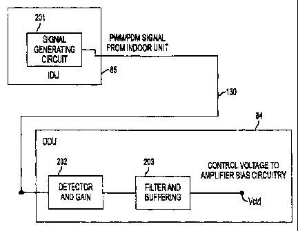
I032j Fig. 2(a) is a block diagram of an exemplary system in accordance with
the
present invention, which allows for active control of an output amplifier
located in an
Outdoor Unit (ODU) by means of a control signal generated in alt Indoor Unit
(IDU).
Referring to Fig. 2(a), the system comprises an IDU 85, which includes a
signal
generating circuit 201 utilized to generate the pew~r control signal; an
lntarfacility link
(lFL) cable 130 that connects the IDU to an ODU 84. The ODU t34 comprises a
detection and gain circuit 202 and a filter and buffering circuit 203, which
as explained in
more detail below, function to detect and process the power control signal
forwarded by
the IDU 85 so as to provide a control voltage to an apparatus (not shown in
Fig. 2(a))
utilized to vary the RF amplifier bias,
[033] In the preferred embodiment of the present invention, the power control
signal
g6~nerated by the tDU 85 is a pulse width modulated (PWM) or pulse density
modulated
signal (PAM). Aa explained i~ more detail below, the duty cycle of the
modulated signal
is variable (under operator control) and is proportional to the required
output power level
6
CA 02365435 2004-10-06
of the RF amplifier. As stated, the power control signal is coupled to the
detection and gain
circuit 202 of the ODU 84. In the given embodiment, the detection and gain
circuit 202
functions to produce a constant voltage signal having a level which
corresponds to the duty
cycle of the power control signal. In other words, as the duty cycle of the
power control
signal is varied, so is the voltage level of the signal output by the
detection and gain circuit
202. Thus, the voltage signal output by the detection and gain circuit 202
comprises a voltage
signal which varies between fixed limits proportional to the duty cycle of the
power control
signal. The output of the detection and gain circuit 202 is then coupled to
the filtering and
buffering circuit 203, which functions to filter/convert the signal output by
the detection and
gain circuit 202 so as to make the signal compatible with the bias circuitry
utilized to alter the
amplifier bias of the output amplifier of the ODU. The output of the filtering
and buffering
circuit 203 corresponds to control signal Vctrl (or Vctrll and Vctrl2). It is
noted that it may
be possible to omit the filtering and buffering circuit 203, assuming the out
of the detection
and gain circuit 202 is compatible with the RF amplifier biasing circuitry.
[034] Fig. 2(b) is a block diagram of an exemplary signal generating circuit
201 contained in
the IDU 85. In the given embodiment, the signal generating circuit comprises a
pulse density
generator 210, which receives the following input signals: (1) a data word,
which corresponds
to the desired output power level of the amplifier, and (2) a clock signal,
fe. The signal
generating circuit further comprises a modulator 212, which includes in the
given example,
an AND gate 214 and a multiplexer 216. The operation of the signal generating
circuit 201 is
as follows.
[035] First, a data word corresponding to the desired output power level of
the amplifier is
input into the pulse density generator 210. It is noted that the data word is
defined by the
operator and is variable under operator control. Upon receipt of the data
word, the pulse
density generator 210, which can be, for example, a sigma-delta modulator
comprising an
accumulator, generates an output signal having a pulse duration corresponding
to the value of
the data word. More specifically, assuming the sigma-delta modulator contained
in the
accumulator has a size equal to N, the output signal of the sigma-delta
modulator comprises
pulses having a density equal to (the value of the data word)/N. For example,
if the data word
input into the sigma-delta modulator equals S and N equals 10, for a cycle
corresponding to
the data size of 10, the output of the
7
CA 02365435 2004-10-06
sigma-delta modulator will be "high" for half the cycle, lithe data word is
increased to "7",
the output of the sigma-delta modulator will be "high" for 7/10 of the cycle.
Similarly, if the
data word is reduced to 1, the output of the sigma-delta modulator will "high"
for 1/10 of the
cycle. Accordingly, by simply adjusting the value of the data word input to
the sigma-delta
modulator, it is possible to adjust the pulse density of the output signal
over a given cycle. It
is noted that sigma-delta modulators are well known in the art and are
therefore not described
in further detail herein.
[036] The output of the sigma-delta generator is coupled to the modulator 212.
More
specifically, the output signal of the sigma-delta generator is coupled to the
AND gate 214
which functions to gate the output signal in accordance with the clock
frequency, fe. The
output of the AND gate 214 is then coupled to the multiplexer 216, which
functions to place
the pulse density modulated signal (PDM) output by the sigma-delta modulator
onto the IFL
130.
[037] To summarize, the PDM signal output by the modulator 212 has a pulse
density (i.e.,
duty cycle) which varies proportionally with variations in the data word input
to the pulse
density generator 210. As explained in further detail below, upon receipt of
the PDM signal,
the ODU, in one embodiment, detects and filters the PDM signal, for example,
utilizing a
low-pass filter so as to generate a power control signal having a voltage
level which varies
proportionally with variations in the pulse density of the PDM signal. The
power control
signal is then utilized to control the power output level of the amplifier, as
explained in more
detail below.
[038] It is noted that circuits and techniques for generating the PWM signal
or the PDM
signal are well known. The foregoing embodiment is intended to be exemplary in
nature, and
in no way limiting. Clearly, other methods of generating a PDM signal or a PWM
signal
exist, and can be utilized in conjunction with the present invention.
[039] Similarly, circuits for receiving and demodulating a PDM signal so as to
output a
voltage level corresponding to the duty cycle are also well known. Any such
circuit can be
utilized for the detection and gain circuit 202 of the ODU 84. As stated, the
output of the
detection and gain circuit 202 is a voltage (or current) signal having an
amplitude (or value)
which varies proportionally with variations in the data word input into the
signal generating
circuit 201.
8
CA 02365435 2001-12-19
Attorney Docket Pa-200361
Customer No. 2pa91
(040J Finally, the design of the filtering and buffering circuit 203 will vary
in accordance
with variables, such as, the type of logic utilized in a given design, the
design of the RF
amplifier, etc. However, the filtering and buffering requirements of a given
design wits be
readily apparent to one of skill in the art upon selection of the othRr iDU
and ODU
components. in addition, it is further noted that other modulation schemes for
modulating the power control signal so as to indicate the desired amplifier
output level
are possible. The PWM and PDM schemes disclosed herein are intended to bar
illustrative and not limiting.
[0411 It is further noted that the variable control methodldevice of the
present invention
can operate in any one of several different modes. For example, the lDU 85 can
be
programmed to set RF amplifier output power level during system set up so as
to
maintain the most efficient power consumption usage of the RF amplifier, based
for
example on location of the terminal (l.e., ODU). An alternate example allows
constant
variation cf the RF amplifier output pow~r lava! based on fa4dback to the IDU
from a
received sipnai from a satellite or other sources (e.g., a phone line).
(042J Fig. 3(a) is an exemplary circuit diagram of a first embodiment of the
control
circuitry for providing active control of an amplifier in accordance with the
present
invention. The control circuitry, which is coupled to an amplifier t0 (e.g., a
field-effect
transistor (FET',) comprises a comparator 12, a series resistor 14 and a
voltage source
16 (Vdd).
[o43J As shown in Fig. 3(a), the amplifier 10 has a source terminal 17 coupled
to
ground potential, a drain terminal 18 coupl~sd to a first input 19 of the
comparator 12 and
to ono Qnd of the soriss resistor 14, and a gate iarminal 11 which is aouplod
to an output
of the comparator 12. The other end of the bias resistor 14 is coupled to the
supply
voltage 16, Vdd. The eomparator 12 comprises a second input 13, which is
coupled to a
voltage control signal line. In the given embodiment, the second input 13 is
coupled to
the output of the filtering and buffering circuit 2Q3. It is noted that while
not shown in
Fig. 3(a), additional feedbacklbias circuitry would be coupled, for example,
to the
comparator 12. However, as the use of such circuitry would be known by those
of skill
in the ari, and would vary from application tv application in accordance with
design
variables, such as, desired bandwidth, chaired rangy of frequency operation,
etc.,
particulars regarding such feedbacklbias circuitry has been omitted from the
9
CA 02365435 2004-10-06
specification to facilitate understanding of the present invention. It is
further noted that when
the present invention is utilized in a VSAT system, in the preferred
embodiment, all of the
components illustrated in Fig. 3(a) are contained in the ODU 84. However, as
mentioned
above, the means for controlling and/or varying the voltage level of control
signal, Vctrl,
originates in the IDU 85, such that it can be controlled and varied without
having to access
the ODU 84.
[044] The operation of the device illustrated in Fig. 3(a) in now described in
conjunction
with the exemplary load lines illustrated in Fig. 7. In the circuit
illustrated in Fig. 3(a), the
comparator 12 and the amplifier 10 form a feedback loop. As shown, and set
forth above, the
comparator 12 comprises two inputs 13, 19. The first input 19 is coupled to
the drain
terminal 18 of the amplifier 10. The second input 13 is coupled to a control
signal, Vctrl
which is generated by the filtering and buffering circuit 203 of the ODU 84.
As noted above,
Vctrl is directly proportional to the duty cycle of the power control signal
generated by the
IDU 85. The comparator 12, which is typically an operational amplifier,
operates to
continually adjust its output voltage level until the voltage levels of the
signals received at the
inputs 13, 19 of the comparator 12 are equal. In other words, as described in
more detail
below, the comparator 12 will continually adjust its output voltage level,
which corresponds
to the gate voltage, Vg, of the amplifier 10, until the drain voltage, Vd, of
the amplifier 10
equals the voltage of the control signal, Vctrl.
[045] As a result, if it is desired to reduce the output power level of the
amplifier 10, the
voltage level of control signal, Vctrl, is increased, which results in an
increase in the drain
voltage, Vd, thereby resulting in a decrease in the voltage drop across
resistor, Rl, and a
corresponding reduction in the drain current, ld. Accordingly, if the supply
voltage 16
remains constant, a reduction in the drain current, ld, reduces the output
power of the
amplifier 10. Of course, the opposite is also true, namely, a reduction in the
control signal,
Vctrl, would result in a decrease in Vd, and a corresponding increase in drain
current, ld,
thereby resulting in an increase in the output power of the amplifier 10.
[046] Thus, the present invention allows for continuous, analog control of the
output power
level of the amplifier 10 simply by adjusting the voltage level of control
signal, Vctrl, which
in the current embodiment is accomplished by adjusting the duty cycle of the
power control
signal generated by the IDU 85. It is also noted that the maximum
CA 02365435 2001-12-19
Attorney Docket PD-20381
Customer No, 20981
output power levels are determined by me saturation characteristics of the
selected
amplifier 10.
(Oa7] It is further noted that Fig. 3(a; only illustrates the DC bias
confiquratian of the RF
amplifier. This bias circuitry is decoupled from the RF amplifier at RF
frequencies using
an RF choke and decoupling capacitors or equivalent microstrip configurations
and
using DC blocking capacitors at the input and output of the amplifier so as to
allow the
RF signal to be AC coupled in and out of the RF amplifier.
(048] Turning again to the device of Fig, 3(a), it is noted that the value of
the current,
Id, is
11
CA 02365435 2004-10-06
governed by the following equations:
ld=gmVgs (1), and
ld=(Vdd - Vd)/R1 (2)
where gm equals the transconductance parameter of the amplifier. Given the
foregoing
equations, it can be readily shown that the gate-source voltage, Vgs, of the
amplifier 10 and
the source-to-drain voltage, Vds, move in opposite directions of one another
in the device of
Fig. 3(a). In other words, as Vds increases (goes more positive), Vgs
decreases (more
negative), and vise versa. Fig. 3(b) illustrates the relationships between
signals, Vctrl, ld,
Vds and Vgs. To summarize, as Vctrl increases, Vds also increases, while ld
and Vgs
decrease. Of course, the opposite is also true, if Vctrl is decreased, Vds
decreases, while ld
and Vgs increase (i.e., less negative, but not greater than 0 volts).
[049] Fig. 7, which illustrates an exemplary load line associated with the
device of Fig. 3(a),
is helpful in understanding the operation of the given embodiment of the
present invention.
As stated above, the output power level of the device of Fig. 3(a) is
adjustable in an
continuous/analog manner by varying the voltage level of the control signal,
Vctrl. Referring
to Fig. 7, load line 60 is an exemplary representation of a load line
corresponding to the
maximum allowable output of amplifier 10, and is referred to as the nominal
bias line. As is
known, load line 60 is determined in-part in accordance with the value of Vdd
coupled to the
resistor 14, RL. As is also known, the maximum value of ld varies in
accordance with the
value of Vgs. As shown in Fig. 7, as Vgs increases, the maximum value of ld
also increases
(i.e., the saturation level), resulting in an increase in the voltage drop
across RL and an
increase in the output power of the amplifier 10. The value of ld
corresponding to load line
60 is illustrated as waveform 61 in Fig. 7. It is noted that Vd also has a
nominal value
corresponding to load line 60, which is depicted as waveform 62 in Fig. 7.
[050] Alternatively, as Vgs decreases, the maximum value of ld also decreases,
thereby
reducing the output power of the amplifier 10. As shown in Fig. 7, a reduction
in Vgs results
in a reduction of the saturation current level of the amplifier 10, and
therefore a reduction in
the maximum allowable value of ld. in other words, a reduction in Vgs
generates a new load
line 63 having a different slope from the nominal load line 60. Referring to
waveform 64, it
is shown that the reduction in Vgs results in a
12
CA 02365435 2001-12-19
Attorney Docket PD-2t)0361
Customer No. 20991
corresponding reduction in the maximum available drain current, Id, and
therefore a
reduction in the output power of the amplifier 1 U. It is further noted that
tt~e voltage
waveform 62 remains unchanged in the current embodiment.
(051,J Accordingly, by use of the feedback loop formed by the comparator 12
and the
amplifier 7 0 it is possible to precisely and continuously cantrvUvary the
output power
level of the amplifier 10 by simply varying the voltage level of signal,
Vctrl. More
specifically, in the event it was desirable to lower the output power of the
device,
assuming that the waveform 61 of Fig, 7 represented the current state of the
device, the
control voltage signet, Vctrl, would be increased, which causes a
corresponding
decrease in Vgs and a.corresponding increase in Vd, as a result of the
feedback loop
which operates to make Vetrl and Vd equal to one another. As a result of the
increase
in voltage, Vd, the drain current Id decreases, The output power is
proportional tv Id' at
the output at RF frequencies. Therefore, if Id decreases while Vd remains
approximately
constant the output power of the amplifier is reduced.
[052] Alternatively, if it is desired to raise the output power of the device,
the voltage
level of Vcrtl is decreased, which causes a corresponding~ineraasa (i.e., less
negative)
in Vgs and a corresponding decrease in Vd, as the feedback loop operates to
make
Vctrl and Vd equal to one another. As a result of the decrease in voltage, Vd,
the drain
current, Id, increases. The output power is propcrtional to Ids at the output
at RF
frequencies. Therefore if Id increases while Vd remains approximately constant
the
output power of the amplifier is increased.
(053J dig. 4(a) illus~.rates a secor?d embodiment of the control circuitry for
providing
active control of the amplifier in accord&nce with thr~ present invention. The
control
circuitry of the second embodiment is identical to the first ernbodimQnt shown
in Fig.
3(a) in all respects except that a variable voltage supply 31 replaces the
fixed power
supply 1 fi coupled to the resistor 14. As such, in the current embodiment,
the supply
voltage 31 coupled !o the resistor 14 is also variable under user control. By
varying the
supply voltage 31, it is also possible to vary the voltage, Vd, at the drain
terminal 18 of
the amplifier 10, thereby allowing a desired increase ar decrease In drain
current, Id,
and the corresponding increase or decrease in the cutput power of the
amplifier 10.
[034] Referring to Fig. 4(b), it can be readily shown that In the event It is
desirable to
lower the power output of the amplifier 10, the control voltage signal, Vctri,
would be
13
CA 02365435 2001-12-19
Attorney Docket PD-200361
Customer No. 20991
increased and the variable supply voltage 31, would ba decreased. As a result,
both the
drain current, Id, and the drain vohage, Vd, are reduced, and Vgs remains
essentially
constant, as shown in Fig. 4(b). Thus, there is a redut~tion in the output
power of the
ampiii7er 10. Alternatively, if it it desired to raise the output power of the
amplifier 10,
the voltage level of Vctrl is decreased and the variable supply voltaga3l is
increased,
which causes a corresponding increase in drain current, Id, and drain voltage,
Vd, and
therefore an increase in the output power of the amplifier 10. Once again, Vgs
remains
substantially constant.
[055j As stated, the circuit of Fig. 4b utilizes another variable control
voltage signal,
Vpos, which is also proportional to the duty cycle of the power control signal
generated
by the IDU. Examples of circuitry used to control.vary Vdd are set forth in
Fig. 5 and Fig
6. As explained in more detail below, the embodiment of Fig 5 utiiixes the
voltage
control cignal Vctrll through a follower circuit after a linear regulator to
vary Vdd. it is
noted that the voltage control signal Vctrt2 corresponds to signal Vctrl of
Figs. 3 and 4.
The embodiment of fig. 6 utilizes the signal Vctrtl to directly alter the
linear regulator
Qutput by adjusting the feedback input to the linear regulator. In one
embodiment, Vpos
is generated in the toll in the same manner as the power Control signal
described
above.
(~56~ Referring to Fig. 8, which illustrates an exemplary load line associated
with the
device of Fig. 4(a), it is shown that by allowing a reduction in both the
drain current, ld,
and the drain voltage, Vd, the original load line 70 Is shifted, bui the slope
of the load
lino romaine constant. The shifted load line Is represented by element 72 in
Fig. 8. The
reduction in drain current. Id, and drain voltage, Vd, which aaucac the shift
in the toad
line, results in a reduction in the maximum available drain current signal 73
and drain.
voltage signal 74, in comparison to the nominal values of the drain current
signal 75 and
the drain voltage signal 78. As such, the output power of the amplifier f0 is
reduced.
(057) In addition; as also shown in Fig. 8, the embodiment of Flg. 4(a)
provides the
additional advantage of moving the bias point of the amplifier 10 away from
the device
breakdown point as the saturation point is reduced, as well as allowing RF
amplifiers
with stabilization resistors on the device gate to be power controlled. This
is particularly
important ae some RF amplifier manufacturers use gate stabilization resistors
to limit the
range of gate voltage applied to the FET. In this situation the device shown
in the first
14
CA 02365435 2004-10-06
embodiment of the present invention, which controls the gate voltage only, an
RF amplifier
with a gate stabilization resistor may be intolerant to the voltage variation
from the bias
circuit at the gate, and hence only a limited variation of ld and hence output
power could be
achieved. The second embodiment using the drain voltage control allows ld to
be varied
sufficiently to allow output power to vary correctly even in the presence of a
gate
stabilization resistor on the RF amplifier.
[058] As stated previously, Fig. 5(a) illustrates an example of how Vdd may be
varied for the
present invention shown in Fig. 4(a). In particular, the embodiment of Fig.
5(a) illustrates a
first exemplary circuit for controlling variations in the supply voltage 31
coupled to the load
resistor, RL. Referring to Fig. 5(a), the circuit comprises the same
components as the first
embodiment of the present invention illustrated in Fig. 3(a), along with a
variable power
supply circuit 41 coupled to the resistor 14. The variable power supply
circuit 41 comprises a
follower circuit 42 coupled to the voltage supply side terminal of the
resistor 14 and a power
supply circuit 43. The follower circuit 42 comprises an operational amplifier
44 and a
transistor 45. As shown, the output of the operational amplifier 44 is coupled
to the base
terminal of transistor 45, and one input to the operational amplifier 44 is
coupled to the
emitter terminal of the transistor 45. The other input to the operational
amplifier 44 is
voltage control signal, Vctrl 1. The collector terminal of the transistor 45
is coupled to the
output of the power supply circuit 43, which is operative for generating a
supply voltage.
[059] As shown, the power supply circuit 43 comprises a linear regulator 46,
and receives a
positive supply voltage as an input. The power supply circuit 43 functions to
produce a
stable output voltage, the level of which is determined in-part by biasing
resistors 47, which
operate to determine the set point of the linear regulator 46. As stated, the
output of the linear
regulator 46 is coupled to the collector of the transistor 45 of the follower
circuit 42.
[060] Fig. 5(b) illustrates the basic operation of the embodiment of the
present invention set
forth in Fig. 5(a). To summarize, the follower circuit 42 operates such that
the voltage
present at the emitter of the transistor 45 tracks the changes in the input
signal, Vctrl 1. More
specifically, in one embodiment, the operational amplifier 44 functions
essentially as an unity
amplifier, wherein the output of the operational amplifier 44 substantially
equals the input
signal Vctrl 1. As the output of the operational amplifier
CA 02365435 2001-12-19
Attorney Docket PD-200361
Customer No. 20991
44 is coupled to the base terminal of transistor 45, the value of Vctrl 1 is
controlled such
that transistor 45 is always vn. Accordingly, the voltage lave) of Vpos is
equal to Vctri 1
minus Vbe of transistor 45, which is essentially fixed. Thus, Vpos essentially
tracks
Vcfrl 1. As a result, if it is desired to raise the voltage level of Vpos,
this is accomplished
by raising the voltage level of Vctrl 1, and if it is desired to lower the
vflltage level of
Vpos, this is accomplished by lowering the voltage level of Vctrl 1. Thus, the
follower
circuit 42 in conjunction with the linear regulator 43 allow the voltage
level, Vpos,
supplied to the load resistor 14 of the amplifier 10 to be varied by simply
varying the
voltage level of control signal Vctrl 1.
[061] Accordingly, referring again to Fig. 5{b), it can be readily shown that
in the event
it is desirable to lower the power output of the amplifier 10, the control
signal, Vctrll ,
would be decreased and the control voltage signal, Vctrl 2 would be increased.
It is
notod that control voltage, Vctrl 2 of Fige. 6(a) and 6(b) corresponds to the
control
signal, Vctrl I, illustrated in Figs. 3(a) - 4(b). As a result, the drain
supply voltage, Vpos,
the drain voltage, Vd and the drain current, Id, are reduced, and Vgs remains
essentially
constant, as shown in i=tg. 6(b). Thus, there is a reductiorf on the output
power of the
amplifier 1 Q. Alternatively, if it is desired to raise the output power of
the amplifier 10,
the voltage level of control signal Vctrl 1 is increased and the voltage level
of control
signal Vctrl 2 is decreased, which causes a corresponding Incraasa in the
drain supply
voltage, epos, me drain voltage, Vd and the drain current, Id, and therefore
an increase
in the output power of the amplifier 10. Once again, Vgs remains substantially
constant.
[062] Fig. 6(a) illuctratos a variation of the devise illustrated in Fig.
b(a). Specifically,
as shown in Fip. fi(8), in this embodiment the follower circuit 42 is omitted
and control
signal Vctrl 1 is directly utilized to vary the drain supply voltage, Vpos,
Generated by the
power supply circuit 52. As shown, the power supply circuit 52 of the current
embadlmant Is essentially the same as the power supply circuit 43 of the third
embodiment,, with the exception that an additional resistor 51 is caupied in
parallel with
the bias resistor 47. The embodiment of Fig. 6{a) provides an advantage over
the
embodiment illustrated in Fig. 5(a) in that it requires a lower component
count and is
therefore less costly to irnpiement.
[063] Referring again to Fig. 6{a), as stated control signal, Votrl 1, is
coupled to the bia3
resistors 47 of the linear regulator 46 via resistor 51. Accordingly, by
raising or lowering
16
CA 02365435 2001-12-19
Attorney Docket Pp-200361
Customor No. 20991
the voltage of Vctrl 1, It is possible to adjust the bias set paint of the
linear regetlatar 46,
and thereby adjust fhe output voltage of the linear regulator, which recruits
in the
adjustment of the drain supply voltage, Vpos. The output voltage of the
regulator is set
by the input at the feedback pin and governed by the following eqcration:
V~ = i .24(i + R' ) _
8
where referring to Fig 6(e): R,, _ ,Ki , and
R~ = R2~R3
Vctrll is a voltage proportional to Vctrl2 and which starts at OV. Vcirii is
set at R3. As
Vctrli is increased from OV, the affect is to make the value of R3 increase
(it is noted
that the actual value of R3 does not change, only the current b~ing drawn
through R3 is
reduced, however to the feedback pin of the regulator the affect is the same
as R3
increasing). In the equation above, if R3 increases this increases the
parallel
combination Rb. Therefore Vout is reduced as Rb increases. The opposite is
also true
as Vcirii falls Rb decreases, Vout Increases to a maximum when Vctrll~V.
[064] Thus, referring to Fg 8(b), in a manner similar to the
ernbodiment_itlustrated in
Fig_ 5(a), if it is dQSirable to lower thQ power output of the amplifiQr 1 b,
the control
voltage signal, Vctrli, would be increased and the control voltage. Vctrl 2,
would be
increased. The increase in Vctrl 1 results in a decrease in the output voltage
of the
linear regulator 46. As a result, the drain supply voltage, Vpos, the drain
voltage, Vd
and the drain current, td, are reduced, and Vgs remains essentially constant,
as shown
in Fig. 8(b). Thus, there is a reduction on the output power of the amplifier
70.
Alternatively, if it is desired to raise the output power of the amplifier 10,
the voltage
level of Vctrl 1 is decreased and the voltage IeYel of Vctn 2 Is decreased,
whlcfi causes
a corresponding Increase in the output voltage level of the linear regulator
48. As a
result, tho drain supply voltage, Vpos, tho drain voltago, Vd and the drain
currant, Id, are
increased. and therefore the output power level of the amplifier 10 is
increased. Once
again, Vgs remains substantially constant.
[0651 As stated above, one of the intended uses of the present invention is to
provide
variable and continuous control of the RF output power amplifier contained in
an ODU of
a VSAT system. Fig. 9 depicts a black diagram of an exemplary VSAT that could
utilize
17
CA 02365435 2001-12-19
Attorney Docket PD-2003fi1
Customer No. 24991
the present invention. Referring to Fig. 9, a typical VSAT system comprises a
remote
ground terminal 89 comprising a small aperture antenna 82 for receiving (i.e.,
downlink)
and transmitting (i.e., uplintc) signals to a satellite 83; the outdoor unit
84 typically
mounted proximate the antenna 82 which cornprisos a transmitter modul~
(including the
RF output power amplifier) for amplifying a modulated data signal which is
coupled to
the antenna 82, and the indoor unit 85 which operates as an interface between
a
specific user's communication equipment and the outdoor unit 84. The lDU is
coupled to
the QDU via an interfacility link 130. The remote ground terminal functions to
transmit
and receive data from a central hub 87 via the satellite 83.
[066J In accordance with the present invention, the components illustrated in
Figs. 3(a),
4(a), 5(a) and 6(a) would typically be l4cated in the ODU 84 of the system, as
the
amplifier 10 under control would corres~nd to the RF power amplifier utilized
to amplify
the signal to be transmitted via the antenna 82. However, as stated, both
control
signals, Vctrll and Vctrl2, would be generated under control of components in
the IDU
85 and the control signals would be coupled to the ODU 84 via the
interfacility link 13p.
This allows the user to actively and continuously control the output power
level of the
amplifier wiihaut having to physically access the ODU 84.
[067], It is further rued that in a typical application, a VSAT system
utilizing the present
invention is initially calibrated to determine the necessary current level
corresponding to
desired maximum power level to be generated by the amplifier during operation.
Qnce
this maximum current (voltage) lave! is determined, it can be readily
determined how to
reduce the currant (voltage) supplied to the amplifier to obtain the desired
output power
19V61. Again, this is due to the fact that the amplifier of the present
invention is operating
in the saturated made, which results in proportional variations between input
current .
(voltage) and output power.
[068] As described above, the method and apparatus for providing active
control of an
amplifier in accordance with the present invention provides important
advantages over
the prior art. Most importantly, this method allows a low cost simple analog
circuit
approach to be used in the oDU rather than a complicated and more expensive
digital
solution using a microprocessor, a Universal Asynchronous Receive Transmit
(UART)
block and mamery.
18
CA 02365435 2001-12-19
Attorney Docket PD-200361
Customer No, 20991
j069J 1n addition, by allowing the output of th8 amplifier to be continuously
varied, the
averafl system operates with increased efficiency, as the amplifier can be
continuously
adjusted to operate slightly above the minimal requirement necessary for
proper
opQration. Also, thQ method allows for open loop or closed loop operation.
Further, the
RF amplifier follows a predictable relationship between DC bias and 8F output
power,
giving the benefit of requiring no calibration during or after manufacture and
allowing
open loop operation.
[070j Yet another advantage of the present invention is that it allows the
gain of the
amplifier to be easily controlled by varying a control signal generated within
the iDU,
thereby negating the need to access the ODU.
[071] in addition, the present Invention allows the output power level of the
t~mpliTter to
be s~t to any level between 0 and a predetermined maximum output level quickly
and
easily, by simply varying the volts~ga levels of ttto control signals,
(Q72] Numerous variations of the various embodiments of the preserst invention
set
forth herein are also possible. For example, the present invention can be
utilized to
control the output power level of essentially any type of arxtplifier,
including but not
limited to, RF amplifiers, optical amplifiers, microwave amplifier; etc.
[Q73J Of course, it should be understood that a wide range of other changes
and
modifications can be made to the preferred embodiment described above. It is
therefore
Intended that the foregoing detailed description be regarded as illustrative
rather than
limiting and that it be understood that it is the following claims including
all equivalents,
which arp intondod to define the scope of the invention.
19