Note: Descriptions are shown in the official language in which they were submitted.
CA 02365454 2004-09-23
27879-166
- 1 -
SEMICONDUCTOR PHOTODETECTION DEVICE
BACKGROUND OF THE INVENTION
The present invention generally relates to
optical semiconductor devices and more particularly to
a semiconductor photodetection device used especially
for fiber optics communication system.
FIG.1 shows in general the structure of a
1o conventional semiconductor photodetection device 10 of
the type that receives incoming optical signal at a
substrate surface side.
Referring to FIG.1, the semiconductor
photodetection device 10 is constructed on a substrate
11 of n-type InP, and includes a layer structure
having an n-type InGaAs optical absorption layer 12
with low carrier concentration formed on the substrate
11 and a cap layer 13 of n-type InP formed on the
layer 12. A p-type InGaAs region 16 and p-type InP
2o region 15 are formed in the InGaAs optical absorption
layer 12 and.the n-type InP cap layer 13 by
introducing a p-type impurity through an opening,
which has been patterned in a dielectric protection
layer 14 formed on the cap layer 13. An n-type
electrode 17 is formed on the n-type InP substrate 11
and a p-type contact electrode 18 is formed on the p-
type InP region 15, respectively. In the n-type
electrode 17 is formed an optical window, through
which an optical signal passes. In this illustrated
3o embodiment, an antireflection film 19 is formed at the
CA 02365454 2001-12-18
- 2 -
optical window on the substrate 11.
In operation of the photodetection device l0
shown in FIG. l, a reverse bias voltage is applied
between the electrodes 17 and 18. Under this
condition, an optical signal having a wavelength of
1260-1620nm used for fiber optics communication enters
into the substrate 11 through the optical window.
Because the substrate InP layer 11 is transparent to
the light having the above wavelength, the incident
to signal light reaches the InGaAs optical absorption
layer 12 without being absorbed by the substrate 11,
and there occurs excitation of photocarriers in the
optical absorption layer 12.
The frequency response of such a semiconductor
i5 photodetection device is generally determined by a
time constant CR and a transit time of the carrier
excited by the incident light, where C is a
capacitance and R is an internal resistance of the
device. In order to improve the frequency response of
20 the semiconductor photodetection device 10, the time
constant needs to be shortened and the carrier transit
time also needs to be shortened. Because the carrier
transit time increases proportionally to the thickness
of the InGaAs optical absorption layer 12, it should
2s be reduced in thickness, as much as possible in order
to shorten the carrier transit time to improve the
frequency response.
However, if the thickness of the InGaAs optical
absorption layer 12 is reduced with the aim of
3o achieving high speed, the optical absorption layer 12
can not absorb the incident light sufficiently, which
degrades the quantum efficiency of the optical
absorption.
Thus, because there exists a trade-off
35 relationship between the frequency response and the
quantum efficiency, it is difficult to obtain the
optimum thickness of the InGaAs optical absorption
CA 02365454 2001-12-18
_ _ 3 _
layer 12 when designing semiconductor photodetection
devices requiring high-speed response.
In order to solve this efficiency problem,
in the conventional semiconductor photodetection
device 10 of the substrate-side incident type shown in
FIG. 1, the signal light that has not been absorbed by
the optical absorption layer 12 is reflected by the p-
type contact electrode 18 and re-introduced into the
optical absorption layer 12 through the InP cap layer
io 13 to avoid the reduction in the quantum efficiency.
In the semiconductor photodetection device
shown in FIG. 1, while a metal layer constituting
the contact electrode 18 is vapor-deposited on the n-
type InP cap layer 13, heat resulting from the vapor-
deposition forms an alloy metal layer at the interface
between the InP cap layer 13 and the metal contact
electrode 18. As a result, the planarity of the
interface between the InP cap layer 13 and the contact
electrode 18 is degraded. This degradation of
2o planarity significantly lowers the reflectivity of the
interface and reduces the amount of the signal light
reflected by the interface, and therefore the signal
light is mostly scattered by the interface and cannot
be absorbed well enough in the InGaAs optical
absorption layer 12. Consequently, the quantum
efficiency is lowered and the amount of light
returning from the photodetection device 10 to an
optical fiber is increased, resulting in lower the
transmission characteristics of fiber optics
3o communication system.
In order to deal with the above mentioned
problem, there has been a proposal, in Japanese Laid-
Open Patent Publication 5-218488, that a dielectric
layer 20 be interposed between the cap layer 13 and
the contact electrode 18 as shown in FIG. 2, and would
inhibit the alloying reaction between the metal layer
of the contact electrode 18 and the InP layer of the
CA 02365454 2001-12-18
~ - 4 -
cap layer 13. Similar or the same parts in FIG. 2
corresponding to the previously described parts in FIG.
1 are designated by the same reference numerals and
the description thereof will be omitted.
This conventional structure of the substrate
side incident type semiconductor photodetection device
shown in Japanese Laid-Open Patent Publication 5-
218488, however, has suffered from problem in that the
contacting area between the contact electrode 18 and
1o the InP cap layer 13 is reduced because of the
dielectric layer 20, and the adherence between the
metal layer of the contact electrode 18 and the
dielectric layer 20 is not strong enough. Therefore,
there has been a problem that the contact electrode 18
peels off during the manufacturing process, wire
bonding process or flip chip mounting process.
SUMMARY OF THE INVENTION
Accordingly, it is a general object of the
2o present invention to provide a novel and useful
semiconductor photodetection device wherein the
foregoing problems are eliminated.
Another and more specific object of the
present invention is to provide a reliable
semiconductor photodetection device having high speed
response and high efficiency.
Another object of the present invention is
to provide a semiconductor photodetection device,
comprising:
3o a semiconductor structure including an
optical absorption layer having a photo-incidence
surface on a first side thereof;
a dielectric reflecting layer formed on a
second side of the semiconductor structure opposite to
the first side;
a contact electrode surrounding the
dielectric reflecting layer and contacting with the
CA 02365454 2001-12-18
_ - $ -
semiconductor structure; and
a close contact electrode covering the
dielectric reflecting layer and contacting with the
contact electrode and the dielectric reflecting layer,
the close contact electrode adhering to the dielectric
reflecting layer more strongly than to the contact
electrode.
Another object of the present invention is
to provide a semiconductor photodetection device,
io comprising:
a semiconductor structure including an
optical absorption layer having a photo-incidence
surface on a first side thereof;
a dielectric reflecting layer formed on a
i5 second side of the semiconductor structure opposite to
the first side;
a contact electrode surrounding the
dielectric reflecting layer and contacting with the
semiconductor structure;
2o a dielectric coating layer surrounding the
contact electrode; and
a close contact electrode covering the
contact electrode and the dielectric coating layer and
contacting with the contact electrode and the
25 dielectric coating layer, the close contact electrode
adhering to the dielectric coating layer more strongly
than to the contact electrode.
It is preferable to form the semiconductor
photodetection device so that the dielectric
3o reflecting layer and the dielectric coating layer are
made of fluoride; oxide or nitride including one or
more atoms selected from the group consisting of Si,
A1, Mg, Ti, Zr and Ta.
Another object of the present invention is
35 to provide a semiconductor photodetection device,
comprising:
a semiconductor structure including an
CA 02365454 2004-09-23
27879-166
- 6 -
optical absorption layer having a photo-incidence
surface on a first side thereof;
a dielectric reflecting layer formed on a
second side of the semiconductor structure opposite to
the first side;
a contact electrode surrounding the
dielectric reflecting layer and contacting with the
semiconductor structure; and
a metal reflecting layer formed within a
1o region inside the contact electrode;
wherein reactivity of the metal reflecting
layer with semiconductor material of the semiconductor
structure is lower than reactivity of the contact
electrode with the semiconductor material.
It is preferable to form the semiconductor
photodetection device so that the metal reflecting
layer includes transition metal belonging to any group
of groups 3B through 8B. Further, it is preferable to
form the semiconductor photode.tection device so that
2o the metal reflecting layer includes one or more atoms
selected from the group consisting of Pt, Ni, TiW and
TiN. Further, it is preferable to form the
semiconductor photodetection device so that the metal
reflecting layer comprises a first metal reflecting
. 25 layer having a thickness thinner than the absorption
length at the signal light wavelength, and a second
metal reflecting layer on the first metal reflecting
layer. Further, it is preferable to form the
semiconductor photodetection device so that the first
3o metal reflecting layer includes transition metal
belonging to any group of groups 3B through 8B and the
second metal reflecting layer includes transition
metal belonging to group 1B or 2B. Further, it is
preferable to form the semiconductor photodetection
35 device so that the first metal reflecting layer
includes one or more elements selected from the group
consisting of Pt, Ni, TiW and TiN, and the second
CA 02365454 2001-12-18
s - 7 -
metal reflecting layer includes one or more atoms
selected from the group consisting of Au, Ag and Cu.
Another object of the present invention is
to provide a semiconductor photodetection device,
comprising:
a semiconductor structure including an
optical absorption layer having a photo-incidence
surface on a first side thereof;
a dielectric reflecting layer formed on a
second side of the semiconductor structure opposite to
the first side;
a contact electrode surrounding the
dielectric reflecting layer and-contacting with the
semiconductor structure;
a barrier electrode formed on the periphery
of the dielectric reflecting layer; and
a reflecting electrode covering the
dielectric reflecting layer and contacting with the
barrier electrode and the dielectric reflecting layer.
2o It is preferable to form the semiconductor
photodetection device so that the dielectric
reflecting layer is made of fluoride, oxide or nitride
including one or more atoms selected from the group
consisting of Si, A1, Mg, Ti, Zr and Ta. Further, it
is preferable to form the semiconductor photodetection
device so that the close contact electrode is made of
Ti or A1. Further, it is preferable to have one or
more additional reflecting layers made of dielectric
or semiconductor on the dielectric reflecting layer.
3o Further, it is preferable to form the semiconductor
photodetection device so that the additional
reflecting layers are dielectric layers comprising
fluoride, oxide or nitride including one or more atoms
selected from the group consisting of Si, Al, Mg, Ti,
Zr and Ta, or semiconductor layers including Si or Ge.
Further, it is preferable to form the semiconductor
photodetection device so that the dielectric
CA 02365454 2004-09-23
27879-166
_ g _
reflecting layer has a refractive index of nl and the
additional reflecting layers has a refractive index of
n2, where n2 > nl. Further, it is preferable to form
the semiconductor photodetection device so that the
close contact electrode performs at least partially a
function of reflecting incident light. Further, it is
preferable to form the semiconductor photodetection
device so that the additional reflecting electrode
includes transition metal belonging to group 1B or 2B.
1o Further, it is preferable to form the semiconductor
photodetection device so that the additional
reflecting layer includes one or more atoms selected
from the group consisting of Au, Ag and Cu. Further,
it is preferable to form the semiconductor
photodetection device so that the metal reflecting
layer comprises a first metal reflecting layer having
a thickness less than the absorption length at the
signal light wavelength, and a second metal reflecting
layer on the first metal reflecting layer. Further,
2o it is preferable to form the semiconductor
photodetection device so that the first metal
reflecting layer includes transition metal belonging
to any of groups 3B through 8B and the second metal
reflecting layer includes transition metal belonging
to group 1B or 2B. Further, it is preferable to form
the semiconductor photodetection device so that the
first metal reflecting layer includes one or more
elements selected from the group consisting of Pt, Ni,
TiW and TiN, and the second metal reflecting layer
3o includes one or more atoms selected from the group
consisting of Au, Ag and Cu. Further, it is
preferable to form the semiconductor photodetection
device so that the barrier electrode has a larger area
than the contact electrode. Further, it is preferable
to form the semiconductor photodetection device so
that the contact electrode is a ring shape. Further,
it is preferable to form the semiconductor
CA 02365454 2001-12-18
_ g
photodetection device so that the contact electrode is
formed partially surrounding the dielectric reflecting
layer. Further, it is preferable to form the
semiconductor photodetection device so that the
semiconductor structure is mounted on a semiconductor
substrate and the photo-incidence surface is placed on
the substrate side of the semiconductor structure.
Further, it is preferable to form the semiconductor
photodetection device so that the semiconductor
structure is mounted on a semiconductor substrate and
the photo-incidence surface is placed on a side
opposite to the substrate of the semiconductor
structure. Further, it is preferable to form the
semiconductor photodetection device so that the
semiconductor structure further includes a carrier-
multiplier layer, and the semiconductor photodetection
device is an avalanche photodiode.
According to the present invention, it
becomes possible to improve the total adherence of the
2o electrode by having a dielectric reflecting layer
inside the contact electrode and by having a close
contact electrode mounted on the dielectric protection
layer outside of the contact electrode, wherein the
close contact electrode is made of high adhesive metal.
As a result, it becomes possible to avoid a problem
that the contact electrode peels off during
manufacturing process, wire bonding process or flip
chip mounting process. Further, it becomes possible
to improve the planarity and reflectivity of a
3o reflecting surface by having a metal reflecting layer
inside the contact electrode wherein the metal
reflecting layer has low reactivity with a
semiconductor layer. Further, it becomes possible to
obtain a high reflective mirror with thin layers by
s5 using a metal layer as a reflective layer. As a
result, it becomes possible to improve step coverage,
throughput and reliability of semiconductor
CA 02365454 2001-12-18
' - 1~ -
photodetection device.
Other objects and further features of the
present invention will become apparent from the
following detailed description when read in
conjunction with the attached drawings.
BRIEF DESCRIPTION OF THE DRAWINGS
FIG.1 is a cross-sectional view showing the
construction of a conventional semiconductor
1o ghotodetection device;
FIG.2 is a cross-sectional view showing the
construction of another conventional semiconductor
photodetection device;
FIG.3 shows manufacturing steps of a
i5 semiconductor photodetection device according to a
first embodiment of the present invention;
FIG.4 shows subsequent manufacturing steps
of the semiconductor photodetection device according
to the first embodiment of the present invention;
2o FIG.5 is a cross-sectional view showing the
construction of the semiconductor photodetection
device according to the first embodiment of the
present invention;
FIG.6 is a cross-sectional view showing a
25 part of a semiconductor photodetection device
according to a second embodiment of the present
invention;
FIG.7 is a cross-sectional view showing a
part of a semiconductor photodetection device
3o according to a third embodiment of the present
invention;
FIG.8 is a cross-sectional view showing the
construction of a semiconductor photodetection device
according to a fourth embodiment of the present
35 invention;
FIG.9 is a cross-sectional view showing the
construction of a semiconductor photodetection device
CA 02365454 2001-12-18
' - 11 -
according to a fifth embodiment of the present
invention;
FIG. 10 is a cross-sectional view showing
the construction of an avalanche photodiode according
to a sixth embodiment of the present invention;
FIG. 11 is a cross-sectional view showing
the construction of an avalanche photodiode according
to a seventh embodiment of the present invention;
FIG. 12 is a cross-sectional view showing
1o the construction of a semiconductor photodetection
device according to an eighth embodiment of the
present invention;
FIG. 13 is a cross-sectional view showing
the construction of a photodetection area of a
semiconductor photodetection device according to a
ninth embodiment of the present invention;
FIG. Z4 is a chart showing bonding strengths
of the semiconductor photodetection device shown in
FIG. 9;
FIG. 15 is a cross-sectional view showing
the construction of a photodetection area of a
semiconductor photodetection device according to a
tenth embodiment of the present invention;
FIG. 16 is a chart showing the relationship
between reflectivities and thicknesses of a Ti close
contact layer of the semiconductor photodetection
device shown in FIG. 15.
FIG. 17 is a cross-sectional view showing
the construction of a semiconductor photodetection
3o device according to an eleventh embodiment of the
present invention; and
FIG. 18 is a cross-sectional view showing
the construction of a photodetection area of a
semiconductor photodetection device according to a
3s twelfth embodiment of the present invention.
DETAILED DESCRIPTION OF THE INVENTION
CA 02365454 2001-12-18
. - 12 -
[FIRST EMBODIMENT]
FIG. 3- (A) through FIG S- (G) show
manufacturing steps of a semiconductor photodetection
device 40 according to a first embodiment of the
present invention.
Referring to FIG.3-(A), the semiconductor
photodetection device 40 is constructed on a substrate
41 of n-type InP, and includes an n-type InGaAs layer
42 formed epitaxially on the substrate 41 and having a
to carrier concentration of 5.5 x 1014 cm-3 and a
thickness of 2um, and an n-type InP layer 43 formed
epitaxially on the InGaAs layer 42 and having a
carrier concentration of 3 x 1015 cm-3 and a thickness
of 1.4~un. The InGaAs layer 42 and InP layer 43 are
is typically formed by the MOVPE method, but can be
formed by other crystal growth technologies such as
the MBE method.
Referring to FIG.3-(B), a dielectric
protection layer 44 typically made of SiN is formed on
2o the InP layer 43 by the CVD method or other deposition
technologies such as sputtering and electron-beam
evaporation, and an opening 44A is made in the
dielectric protection layer 44 by photolithograpic
process. A p-type impurity is introduced into the InP
25 layer 43 through the opening 44A by thermal diffusion
or ion implantation. As a result, a p-type region 45
and a p-type InGaAs region 46 are formed corresponding
to the opening 44A, in the n-type InP layer 43 and at
the top surface of the n-type InGaAs layer 42. The p-
3o type impurity may be Zn, Cd, Be or a like substance.
Referring to FIG.3-(C), a dielectric layer
50 made of SiN or a like substance is formed so that
it covers the dielectric protection layer 44 and the
p-type InP region 45 at the opening 44A. Then the
35 dielectric layer 50 is patterned by photolithographic
process as shown in FIG.4-(D), to form a dielectric
layer pattern 50A on an exposed surface of the InP
CA 02365454 2001-12-18
~ - 13 -
layer 45. As the dielectric layer pattern 50A is
formed, a ring-shaped opening 48A is made around the
pattern 50A to partially expose the top surface of the
p-type InP region 45.
In a subsequent step shown in FIG.4-(E), a
ring-shaped contact electrode 481 having an Au/Zn/Au
layer structure is formed in the ring-shaped opening
48A, by using a vapor deposition process such as
resistance heating vacuum vapor deposition or
1o electron-beam evaporation, and a lift-off process.
Further, the thus formed ring-shaped contact electrode
481 is heated to be alloyed.
Because an alloy layer is made at a ring-
shaped interface area between the p-type InP region 45
and the ring-shaped contact electrode 481 due to the
heat process, the planarity of the InP layer 43
becomes worse at that area. However, the original
planarity of the InP layer 43 is maintained at the
area where the dielectric layer pattern 50A is formed,
2o where a light signal which has passed through the
InGaAs layer 42 reaches and can be reflected well.
Referring to FIG.4-(F), a resist pattern
having an opening exposing the ring-shaped contact
electrode 481 is made on the dielectric layer 50, a
conducting layer made of Ti or A1 is deposited on the
resist pattern and lifted off, to form a close contact
electrode 482 which contacts with the ring-shaped
contact electrode 481 and the dielectric layer pattern
50A.
3o In the above steps, in spite of the heating
alloying process of the contact electrode 481, the
interface between the dielectric layer pattern 50A and
the n-type InP layer 43 maintains the original
planarity because the dielectric layer pattern 50A
does not react with InP.
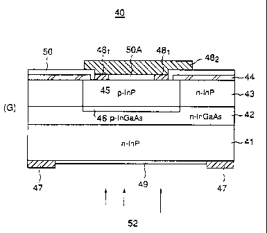
Referring to FIG.5-(G), a ring-shaped n-type
electrode 47 and an antireflection film 49 are formed
CA 02365454 2001-12-18
' - 14 -
on the bottom surface of the n-type InP substrate 41.
When a signal light is introduced into the substrate
41 through the antireflection film 49, the light
signal light is partially absorbed by the InGaAs layer
42 and then reflected by the dielectric layer pattern
50A and returned back into the InGaAs layer 42.
Because the planarity of the interface between the p-
type InP region 45 and the dielectric layer pattern
50A is well maintained, high reflectivity is obtained
io and optical loss is minimized.
In this embodiment, the close contact
electrode 482 made of Ti or A1 which is well attached
by the dielectric layer pattern 50A or the dielectric
layer 50, is formed both inside and outside the ring-
shaped contact electrode 481, therefore, the total
adherence of the electrode including the ring-shaped
contact electrode 481 and the close contact electrode
482 is much improved. As a result, this embodiment
can avoid a problem that the contact electrode peels
off during manufacturing process such as wire bonding
process or mounting process.
The following table comparatively shows the
peeling-off rates of a semiconductor photodetection
device according to this embodiment and a conventional
device as shown in FIG.2. These peeling-off rates
were obtained by performing the tests 1000 times.
Device Peeling-off rate
Conventional device >80%
This embodiment <1%
This table shows that the contact electrode
3o peeled off in more than 80% of the tested conventional
devices while the electrode peeled off in less than 1%
of the tested photodetection devices according to this
embodiment.
As mentioned above, it is possible to use A1
CA 02365454 2001-12-18
' - 15 -
instead of Ti as the close contact electrode 482 in
this embodiment. And it is also possible to use a
fluoride layer or an oxide layer of Si, A1, Mg, Ti, Zr,
Ta or similar substance instead of a SiN layer as the
dielectric layer 50A.
The conductivity types can be reversed from
p-type to n-type in this embodiment. The
semiconductor layers 41-43 are not limited to III-V
compound semiconductor materials and may be Si or Ge.
io
[SECOND EMBODIMENT]
The close contact electrode 482 made of Ti
is disposed on the dielectric pattern 50A placed
inside the ring-shaped contact electrode 481 in the
previous embodiment.
Even though the interface between the p-type
InP region 45 and the dielectric pattern 50A is planar,
the signal light 52 may not be reflected by the
dielectric layer 50A well enough when the reflectivity
of the layer 50A is low. In that case, the light
coming through the dielectric layer pattern 50A
reaches the electrode 482 and is absorbed there to
degrade the absorption characteristics of the device.
This second embodiment has a ~,(lambda)/4
multiple reflecting layer structure which is mounted
on the dielectric layer pattern 50A. ~, is an
incident light wavelength. The ~.(lambda)/4 multiple
reflecting layer structure is formed by laminating
Si02 layers 501 and Si layers 502 alternately as shown
3o in FIG.6. The total reflectivity of the laminated
SiOz layers 501 and Si layers 502 can be increased to
100% by making each of the optical thicknesses of
theses layers set up in 1/4 of the wavelength of the
incident light. As a result, it is possible to
completely avoid the optical absorption by the Ti
close contact electrode 482.
Alternatively, the dielectric layer pattern 50A
CA 02365454 2001-12-18
- 16 -
itself may have such a multiple layer structure shown
in FIG.6. Although the Si02 layers 501 and Si layers
502 are laminated twice in the embodiment shown in
FIG.6, these layers can be laminated even only once,
or three or more times repeatedly. It is preferable
to have a Si02 layer 501 at the top of the laminated
reflecting layers 50A in order to stabilize the
structure. The ~,(lambda)/4 multiple reflecting layer
can be made of other combination materials such as a
1o Si02 layer and a Ti02 layer. And a Ge layer can be
used instead of a Si layer.
[THIRD EMBODIMENT]
FIG.7 shows the construction of a close
contact electrode 482 according to a third embodiment
of the present invention.
Referring to FIG.7, the close contact
electrode 482 of this embodiment has a laminated
structure including Ti layer 482A, Pt layer 482B and
2o Au layer 482C. The lowermost Ti layer 482A can be well
attached to the dielectric pattern 50A. On the other
hand, the uppermost Au layer 482C lowers the contact
resistance and therefore the total resistance of the
close contact electrode 482. Further, the middle Pt
layer 482B interposed between Ti layer 482A and Au
layer 482C suppresses interdiffusion between the
lowermost layer 482A and the uppermost layer 482C.
In this structure shown in FIG.7, the Ti
layer 482A constitutes only a small portion of the
3o electrode 482. The high reflective Pt layer 4828 and
Au layer 482C account for the major portion of the
electrode 482, and therefore the absorption of the
light coming from the dielectric layer pattern 50A by
the Ti layer can be minimized.
[FOURTH EMBODIMENT]
FIG.8 shows the construction of a
CA 02365454 2001-12-18
- 17 -
semiconductor photodetection device 60 according to a
fourth embodiment of the present invention. Those
parts corresponding to the parts described previously
are designated by the same reference numerals and the
description thereof will be omitted.
Referring to FIG.8, the semiconductor
photodetection device 60 has a structure similar to
that of the previously explained semiconductor photo
detectian device 40, but is different from the device
io 40 in that the device 60 has a high reflecting pattern
483 as a metal reflecting layer. The high reflecting
metal layer 483 is placed inside the ring-shaped
contact electrode 481 and covered with the dielectric
pattern 50A, and is typically made of Pt, Ni, TiW or
TiN.
In actual manufacturing process of the
semiconductor photodetection device 60 as shown in FIG.
8, after the formation of the p-type InP region 45 in
the step shown in FIG.3-(B), the Pt pattern 483 is
2o formed on the InP layer 45 inside the opening 44A, and
thereafter the dielectric layer 50 is deposited so as
to cover the Pt pattern 483.
The reflectivity of the dielectric pattern
50A having the multiple layer structure shown in FIG.6
is improved as the repeating time of the layers is
increased. However, the thickness of the multiple
reflecting layer structure 50A is increased at the
same time. Accordingly it becomes difficult to form
the ring-shaped contact electrode 481 in the FIG.4-(E)
3o step, because the ring-shaped opening 48A becomes
deeper. On the other hand, according to this
embodiment of the present invention, the reflecting
pattern 483 itself has high reflectivity, and
therefore it is possible to obtain a high reflecting
mirror of a small thickness without using the multiple
reflecting layer 50A shown in FIG.6.
According to this embodiment of the present
CA 02365454 2001-12-18
- 18 -
invention, it is possible to make the dielectric layer
50 and 50A thinner, and therefore improve the
regularity of the surface of the electrode structure
formed on the InP layer 43. As a result, the step
coverage problem when making the contact electrode 481
and the close contact electrode 482 is alleviated,
resulting in improved throughput and reliability in
the device manufacturing process.
[FIFTH EMBODIMENT]
FIG.9 shows the construction of a
semiconductor photodetection device 80 according to a
fifth embodiment of the present invention. Those
parts corresponding to the parts described previously
are designated by the same reference numerals and the
description thereof will be omitted.
Referring to FIG.9, the semiconductor
photodetection device 80 has a structure similar to
that of the previously explained semiconductor photo
2o detection device 60, but is different from the device
60 in that the high reflecting pattern Pt 483 in the
device 80 directly contacts with the close contact
electrode 482. The dielectric pattern 50A is placed
only in a ring-shaped area between the high reflecting
2s pattern 483 and the ring-shaped contact electrode 481.
This dielectric layer pattern 50A does not
necessarily have to function as a reflecting layer,
and therefore can be omitted so that the high
3o reflecting pattern 483 contacts with the contact
electrode 481.
In this embodiment, because the high
reflecting pattern 483 is made of conductive material
such as Pt, Ni, TiW, TiN or similar substance, its
35 electric resistance is low and the frequency response
of this device is improved.
Although the n-type electrode 47 is formed
CA 02365454 2004-09-23
27879-166
- 19 -
on the bottom surface of the substrate 41 in this
embodiment, it can be alternatively placed on or above
the top surface of the n-type InP layer 43 in order to
obtain higher frequency response. In this case,
solder bumps may be formed on the close contact
electrode 48z for flip chip mounting application.
Considerations of the material for the high
reflecting pattern 483 will be given below.
In order to improve the reflectivity of the
1o reflecting pattern 483 to nearly 100%, the pattern 483
is preferably made of a transition metal element (so
called.noble metal) such as Au, Ag or Cu, belonging to
group 1B or 2B. These metals, different from other
transition metals, have an absorption edge wavelength
i5 of less than 0.6um by the total dielectric effect due
to inter-band transition and free electrons, and
therefore do not absorb light used for optical
communication application.
On the other hand, these metals tend to
20 become thermally diffused into semiconductor layers to
create an alloy, and have inferior adhesive
characteristics because they have only one or two most
outer-shell electrons, and therefore the semiconductor
photodetection device using these metals have
25 reliability problem. Further, thermal stress causes
other problems that the reflectivity varies and the
adhesive strength cannot be maintained when attaching
bonding wires or mounting the device on a circuit
board.
3o For this embodiment of the present invention,
the high reflecting pattern 483 is made of materials
including groups 3B-8B transition metal element such
as Ti, having many most outer-shell electrons, in
order to prohibit the metal diffusion into
35 semiconductor layers and improve the adhesive strength.
On the other hand, these metals belonging to groups
3B-8B exhibit strong absorption of light used for
CA 02365454 2004-09-23
27879-166
- 20 -
optical communication application from the visible
region to the far infrared region due to transition in
band, and may not achieve the desired high
reflectivity.
In consideration of these problems, material
including transition metal elements (such as Au, Ag
and Cu) of group 1B or 2B is deposited on the high
reflecting pattern 483 made of a transition metal
element.of groups 3B-8B for this embodiment of the
1o present invention. The thickness of the layer made of
the transition metal elements belonging to groups 3B-
8B is selected so as to be less than the absorption
length at the signal light wavelength to minimize
optical absorption.
The contact electrode 481 is not limited to
the ring-shape, and may be of other shapes that
partially surround the reflecting pattern 483.
Although the above embodiments were
explained using a substrate side incident type of
2o photodetection device, the present invention can be
applied to a surface incident type of photodetection
device.
[SIXTH EMBODIMENT]
FIG.10 shows the construction of a surface
mounted type avalanche photodiode 100 according to a
sixth embodiment of the present invention, wherein
those parts corresponding to the parts described
previously are designated by the same reference
numerals and the description thereof will be omitted.
Referring to FIG.10, the avalanche
photodiode 100 has a general semiconductor layer
construction similar to the previously described
semiconductor photodetection devices 40-80, and
includes an n-type InGaAs optical absorption layer 42
formed on an n-type InP substrate 41 and an n-type InP
cap layer 43, and further includes an InGaAsP graded-
CA 02365454 2001-12-18
' - 21 -
composition layer 101 doped to n-type between the
optical absorption layer 42 and the cap layer 43..A
p-type region 45 is formed in the cap layer 43, and a
p-type guard ring 45G surrounding the p-type region 45
is formed. The InP cap layer 43 functions as a photo
multiplier layer in this embodiment.
The avalanche photodiode 100 according to
this embodiment has a contact trench 100A dug through
the InP cap layer 43 all the way to the substrate 41.
1o A conductor pattern 100a exists from the bottom of the
contact trench 100A to the top surface of the cap
layer 43, in order to enable surface mounting.
On the surface of the InP cap layer 43, a
dielectric layer 50 made of SiN or similar substance
is formed so as to cover the conductor pattern 100a
and the surface of the contact trench 100A. A
dielectric layer pattern 50A is formed separated from
the dielectric layer 50 by a ring-shaged ogening 48A
(See FIG.4-(D)). A ring-shaped contact electrode 481
2o is formed in the ring-shaped opening 48A.
Further, on the dielectric layer pattern 50A
is formed a close contact electrode 482 typically made
of Ti or A1, having excellent adhesive strength to the
dielectric layer pattern 50A.
2s A contact hall is opened in the dielectric
layer 50 to expose the conductor pattern 100a and an
n-type electrode 47 is formed so as to connect to the
n-type InP substrate 41 via the conductor pattern 100a.
so Also in this avalanche photodiode, the
dielectric layer pattern 50A maintains the original
planarity of the surface of the p-type InP region 45
even after the formation of the close contact elctrode
482. Therefore, light which enters the substrate 41
35 through ari antireflection film 49 and reaches the cap
layer 43 without being absorbed by the optical
absorption layer 42, can be reflected back to the
CA 02365454 2001-12-18
- - 22 -
optical absorption layer 42 with high efficiency and
absorbed there.
The avalanche photodiode according to this
embodiment also may utilize the high reflecting layer
483 previously explained in the semiconductor
photodiode devices 60 and 80.
[SEVENTH EMBODIMENT]
FIG.11 shows the construction of a surface
1o mounted type avalanche photodiode 110 according to a
seventh embodiment of the present invention, wherein
those parts corresponding to the parts described
previously are designated by the same reference
numerals and the description thereof will be omitted.
i5 Referring to FIG.11, the avalanche
photodiode 110 has a lens-like condenser portion 41L
formed at the bottom surface of an InP substrate 41.
Therefore, a light signal incident to the device is
efficiently condensed on the photodetection structure.
Other features of this embodiment are the
same as those of the previous embodiment and the
description thereof will be omitted.
[EIGHTH EMBODIMENT]
FIG.12 shows the construction of a
semiconductor photodetection device 120 of a type that
receives incoming optical signals at a top surface
side according to an eighth embodiment of the present
3o invention, wherein those parts corresponding to the
parts described previously are designated by the same
reference numerals and the description thereof will be
omitted.
Referring to FIG.12, the surface-incident
type semiconductor photodetection device 120 has a
general construction similar to the semiconductor
photodetection device 40 shown in FIG S, but the
CA 02365454 2001-12-18
_ 23 _
dielectric layer 50 and the dielectric layer pattern
50A are replaced by an antireflection film 49, and an
opening 48W is made in a closed contact electrode 482
to expose the antireflection film 49.
In the surface-incident type semiconductor
photodetection device 120 shown in FIG.12, a high
reflecting dielectric layer pattern 50A is formed on
the bottom surface of a substrate 41, and an n-type
electrode 47 is formed at the bottom surface of the
io substrate 41 so as to cover the high reflecting layer
pattern 50A.
In the operation of the semiconductor
photodetection device 120, an incident light 52 passes
through the antireflection film 49 after passing
i5 through a window 48W in the close contact electrode
482, and is then absorbed by an optical absorption
layer 42. A part of the incident light beam which
has not been absorbed is reflected by the high
reflecting layer 50A formed on the bottom surface of
2o the substrate 41 and returned to the optical
absorption layer 42. Because the dielectric layer
50A is formed between the bottom surface of the
substrate 41 and the n-type electrode 47, no alloy is
created between them, and therefore.an excellent
2s reflecting surface is maintained there.
[NINTH EMBODIMENT]
FIG.13 is an enlarged cross-sectional view
of a photodetection area of a substrate-incident type
3o semiconductor photodetection device 130 according to a
ninth embodiment of the present invention. A
semiconductor substrate and electrodes are not shown
in FIG.13.
Referring to FIG.13, the semiconductor
3s photodetection device 130 includes an epitaxially
formed n-type InP layer 132 having a carrier
concentration of 2 x 101' crri 3 and a thickness of l.5um,
CA 02365454 2001-12-18
~ - 24 -
an n-type InGaAs optical absorption layer 133 formed
epitaxially on the InP layer 132 and having a carrier
concentration of 5.5 x 1014 cm 3 and a thickness of 2~.un,
and an n-type InP layer 134 formed epitaxially on the
optical absorption layer 133 and having a carrier
concentration of 6 x 1015 cm-3 and a thickness of l.5um.
A p-type region 134A including Zn, Cd, Be or similar
substance is formed in the InP layer 134 so as to
reach the optical absorption layer 133.
A insulating layer 135 of SiN layer or
similar substance is formed typically by the CVD
method on the InP layer 134 and an opening is made in
the insulating layer 135 to expose the p-type region
134A. A SiN or Si02 dielectric layer 136 having an
i5 optical thickness set up in 1/4 of a signal light
wavelength is formed typically by the CVD method on
the insulating layer 135. The p-type region 134A is
formed by introducing p-type impurity atoms through
the opening in insulating layer 135 and thermally
diffusing them.
Dielectric layer 136 is then patterned, and
a dielectric layer 135A is formed as a mirror on the
p-type region 134A, separated from the dielectric
layer 136 by a ring-shaped trench. In the ring-shaped
trench is formed a ring-shaped AulZn/Au electrode
pattern 137 ohmic-contacting with the p-type region
134A, by the lifting-off method.
In this embodiment, a ring-shaped barrier
pattern 138 is formed on the ring-shaped Au/Zn/An
so electrode pattern 137 by laminating Ti and Pt layers
in turn. An Au pillar 139 is formed on the ring-
shaped barrier pattern 138 by plating and lifting-off
method, so as to contact with the dielectric pattern
135A. A bump electrode 140 of Au/Sn alloy metal is
formed on the Au pillar 139.
In this semiconductor photodetection device,
the ring-shaped electrode pattern 137 ohmic-contacts
CA 02365454 2001-12-18
- - 25 -
with p-type diffusion region 134A and the planarity of
their interface gets worse. However, the interface
between the dielectric mirror pattern 135A and the p-
type diffusion region 134A is planar providing an area,
where the light signal is well reflected.
In this embodiment, the Au pillar 139
functions a refection mirror together with the
dielectric mirror pattern 135A. The Au pillar 139
does not adhere well to the dielectric mirror pattern
135A, but adheres well to the ring-shaped barrier
pattern 138 and therefore the Au pillar 139 is
prevented from peeling off. As previously explained,
the Ti atom has many most outer-shell electrons, and
is strongly bonded to other elements. On the other
i5 hand, Pt functions as a diffusion barrier, which
inhibits Au in the Au pillar 139 from diffusing into
the p-type diffusion region 134A. In this structure,
stable reflectivity is obtained even when the
semiconductor photodetection device 130 suffers
2o thermal stress.
In this embodiment, a TiW layer or TiN layer
can be. used as the ring-shaped barrier pattern 138,
instead of Ti/Pt laminated layers. Further, instead
of Au, another transition metal element belonging to
25 group 1B or 2B such as Ag or Cu or group 3B such as A1
can be used for the pillar 139.
FIG.14 shows the results of a chip bonding
strength test performed on the semiconductor
photodetection device 130.
30 Referring to FIG.14, ~(a square? represents
the result of testing the conventional semiconductor
photodetection device, 1(a solid circle? represents
the result of testing the semiconductor photodetection
device 130.
35 It can be seen from FIG.14 that the bonding
strength of this embodiment, semiconductor
photodetection device 130, is similar to or. better
CA 02365454 2001-12-18
- - 26 -
than that of the conventional semiconductor
photodetection device.
[TENTH EMBODIMENT)
FIG.15 shows the construction of a
semiconductor photodetection device 150 according to a
tenth embodiment of the present invention, wherein
those parts corresponding to the parts described
previously are designated by the same reference
numerals and the description thereof will be omitted.
Referring to FIG.15, a Ti close contact
layer 138A is interposed between a ring-shaped barrier
layer pattern 138 and an Au pillar 139 and between a
dielectric mirror pattern 135A and the Au pillar 139.
i5 This Ti close contact layer makes the bonding strength
of the semiconductor photodetection device 150
stronger.
As previously explained, the Ti layer
absorbs light at the operational wavelength of the
semiconductor photodetection device 150. Therefore,
the thickness of the Ti close contact layer 138A is
arranged to be thinner than the absorption length (the
inverse number of absorption coefficient of the Ti
layer.
FIG.l6 shows the relationships between the
thicknesses and reflectivities at 1550nm and 1620nm
wavelenghs.
Referring to FIG.16, it can been seen that
the reflectivity decreases as the Ti layer gets
thicker. The thickness of the Ti layer should be less
than 40nm in order to obtain a desirable reflectivity
that is equal to or better than the reflectivity (60%)
of a conventional reflection mirror having a laminated
100nm Ti layer and 215nm SiN layer.
Accordingly, in the embodiment shown in
FIG.15, the thickness of the close contact layer 138A
is preferably less than 40nm. For example, a close
CA 02365454 2001-12-18
- 27 _
contact layer 138A having a thickness of 30nm gives a
reflectivity higher than prior devices.
[ELEVENTH EMBODIMENT]
FIG.17 shows the construction of a
semiconductor photodetection device 160 according to
an eleventh embodiment of the present invention,
wherein those parts corresponding to the parts
described previously are designated by the same
reference numerals and the description thereof will be
omitted.
Referring to FIG.17, a dielectric layer
mirror pattern 50A and a dielectric layer pattern 50B
are formed on the bottom surface of a substrate 41 by
i5 patterning dielectric layers thereon. A ring-shaped
Au/Ge/Au ohmic electrode 51 is formed in a ring-shaped
groove between the dielectric layer mirror pattern 50A
and the dielectric layer pattern 50B.
A ring-shaped Ti/Pt barrier electron pattern
52 is formed so as to cross-link the dielectric layer
mirror pattern 50A and the dielectric layer pattern
SOB and to directly contact with the ring-shaped ohmic
electrode 51 interposed between them. An Au electrode
47 is formed on the barrier electrode pattern 52 so as
to contact with the dielectric reflection pattern 50A
through an opening made in the barrier electrode
pattern 52. A bump electrode 53 for mounting purposes
is formed on the Au electrode 47. In this embodiment,
the electrode 47 may be made of transition metal
belonging to group 18 or 2B such as Ag or Cu, which
absorbs less light. An n-type InP buffer layer 41A is
interposed between the InP substrate 41 and the InGaAs
optical absorption layer 42.
In the thus structured semiconductor
photodetection device 160, incident light comes
through a dielectric layer 49 into the substrate 41,
and is reflected by the dielectric mirror pattern 50A
CA 02365454 2001-12-18
_ 28 _
and absorbed by an optical absorption layer 42.
In this embodiment, because the Ti/Pt
barrier electrode 52 is formed on the dielectric layer
patterns 50A, 50B and connected to the Au electrode 47,
s the weak adhesion between the Au electrode 47 and the
dielectric layer mirror SOA is compensated for; and -
therefore the semiconductor photodetection device 160
can be reliably mounted on a circuit board. Because
there is no ohmic contact between the dielectric layer
io mirror pattern 50A and the substrate 41, high
reflectivity is attained.
[TWELFTH EMBODIMENT]
FIG.18 is an enlarged cross-sectional view
15 of a photodetection area of a surface mounting type
avalanche photodiode 170 according to a twelfth
embodiment of the present invention, wherein those
parts corresponding to the parts described previously
are designated by the same reference numerals and the
2o description thereof will be omitted.
Referring to FIG.l8,,the avalanche
photodiode 170 has a structure similar to that of the
previously explained avalanche photodiode 100 shown in
FIG.10, but is different in the following ways. An
25 electrode 482 is made of transition metal belonging to
group 1B or 2B such as Au, Ag or Cu which absorbs less
light. A Ti/Pt barrier electrode 161 is interposed
between the ohmic electrode 481 and the Au layer 482.
An Au/Sn bump for mounting purposes is formed on the
3o electrode 482. An n-type InP buffer layer 41A is
interposed between a substrate (not shown) and an
InGaAs layer 42.
Thus structured the avalanche photodiode 170
can be reliably flip-chip-mounted on a circuit board
35 with high strength. A Ti layer that absorbs light is
used only for the barrier electrode 161, and therefor
the reflectivity of the reflecting region including
CA 02365454 2001-12-18
- - 29 -
the dielectric layer mirror 49 is not lowered.
Each embodiment explained above is a planar
type device in which p-type semiconductors are made by
diffusing impurities. However, the present invention
can be applied to a mesa-type device. Conducting
types can be reversed from p-type to n-type in each
embodiment above. Although the above-explained
embodiments are based on III-V compound semiconductor,
the present invention can be applied to other types of
1o semiconductors such as Si or Ge.
Further, the present invention is not
limited to the embodiments described heretofore but
various variations and modifications may be made
without departing from the scope of the invention.
According to the present invention as set
forth above, it becomes possible to obtain high
adhesive strength of the electrodes including the
contact electrode and the close contact electrode, and
avoid the contact electrode peeling-off problem during
2o the manufacturing process or packaging and mounting
processes including a wire bonding process. Further,
it becomes possible to planarize the light reflection
surface and improve the reflectivity. Further, in the
case of using a metal layer as a reflection mirror,
the thickness of layers becomes small. As a result,
the step coverage problem when forming electrodes is
alleviated and the throughput and reliability when
manufacturing this device is much improved.