Note: Descriptions are shown in the official language in which they were submitted.
CA 02365689 2001-08-29
WO 00/52818 PCT/US00/05184
FM DEMODULATOR USING A DIFFERENTIATOR - -
BACKGROUND OF THE INVENTION
1. Field of the Invention.
This invention relates in general to an FM demodulator, and more
particularly to an FM demodulator circuit and method that has a reduced
sensitivity
to noise which enhances the performance of a system.
2. Description of Related Art
Today's wireless communications markets are being driven by a multitude of
user benefits. Products such as cellular phones, cordless phones, pagers, and
the like
have freed corporate and individual users from their desks and homes and are
driving the demand for additional equipment and systems to increase their
utility.
As a result digital radio personal communications devices will play an
increasingly
important role in the overall communications infrastructure in the next
decade.
Mixed-signal integration and power management have taken on added
importance now that analog and mixed analog-digital ICs have become the
fastest-
growing segment of the semiconductor industry. Integration strategies for
multimedia consoles, cellular telephones and battery-powered portables are
being
developed, as well as applications for less integrated but highly specialized
building
blocks that serve multiple markets. These building blocks include data
converters,
demodulators, filters, amplifiers and voltage regulators.
One important aspect of digital radio personal communications devices is the
integration of the RF sections of transceivers. Compared to other types of
integrated
circuits, the level of integration in the RF sections of transceivers is still
relatively
low. Considerations of power dissipation, form factor, and cost dictate that
the
RF/IF portions of these devices evolve to higher levels of integration than is
true at
present. Nevertheless, there are some key barriers to realizing these higher
levels of
integration.
For example, most applications provide an FM demodulator in an RF
receiver system to recover transmitted data from a carrier signal. For FM
demodulators, robust performance requires a bit error rate (BER) performance
close
to the theoretical performance limit. However, this requires the
implementation of
circuitry which reduces the demodulator's sensitivity to noise.
CA 02365689 2001-08-29
WO 00/52818 PCT/US00/05184
2
It can be seen then that there is a need for an FM demodulator circuit an -
method with reduced sensitivity to noise that provides a low bit error rate
and
performance.
SUMMARY OF THE INVENTION
To overcome the limitations in the prior art described above, and to
overcome other limitations that will become apparent upon reading and
understanding the present specification, the present invention discloses an FM
demodulator circuit and method providing reduced sensitivity to noise and
enhances
the performance of a system almost identically with the theoretical
predictions for an
ideal demodulator.
The present invention solves the above-described problems by providing an
FM demodulator circuit which reduces sensitivity to noise by reducing the bit
error
rate and enhancing the performance of the system.
A system in accordance with the principles of the present invention includes a
discrete-time sampled detector for a binary frequency shift key (BFSK)
modulated
signal. The sampled waveform is provided by an in-phase (I) signal and a
quadrature
(Q) signal output of the receiver, which have been over sampled by a factor of
four
with respect to a data rate. The function of the demodulator is to sense a
direction of
rotation of an I/Q signal constellation in.a Q vs. I plane and to generate an
appropriate
digital output.
Other embodiments of a system in accordance with the principles of the
invention may include alternative or optional additional aspects. One such
aspect of
the present invention is that the system includes a time sampling detector
which
implements a discrete-time period rather than a continuous time period when
sampling the modulated signal input. The discrete-time period makes it
possible to
use a plurality of circuitry, such as switched capacitor and analog circuits.
Those
skilled in the art will understand that the period is not limited to discrete-
time, other
measurements of time, such as continuous time, may be used.
Another aspect of the present invention is that the FM demodulator fiurther
includes an oversampling of the input signals to obtain robust performance in
the
presence of noise.
Another aspect of the present invention is that the FM demodulator further
includes the elimination a low amplitude signal to reduce the sensitivity to
noise in the
in-phase and the quadrature signals.
CA 02365689 2001-08-29
WO 00/52818 PCT/US00/05184
3
These and various other advantages and features of novelty which characterize -
the invention are pointed out with particularity in the claims annexed hereto
and form a
part hereof. However, for a better understanding of the invention, its
advantages, and
the objects obtained by its use, reference should be made to the drawings
which form a
further part hereof, and to accompanying descriptive matter, in which there
are
illustrated and described specific examples of an apparatus in accordance with
the
invention.
BRIEF DESCRIPTION OF THE DRAWINGS
Referring now to the drawings in which like reference numbers represent
corresponding parts throughout:
Fig. 1 is an exemplary diagram showing the FM demodulator in a typical
radio receiver system;
Fig. 2 is a block diagram of an FM demodulator circuit;
Fig. 3 illustrates in greater detail the FM demodulator;
Fig. 4 is a diagrammatic representation of a signal constellation;
Fig. 5 is a flow diagram illustrating method of FM demodulation according
to the present invention; and
Fig. 6 is a digital representation of an FM demodulator circuit.
DETAILED DESCRIPTION OF THE INVENTION
In the following description of the exemplary embodiment, reference is made
to the accompanying drawings which form a part hereof, and in which is shown
by
way of illustration the specific embodiment in which the invention may be
practiced.
It is to be understood that other embodiments may be utilized as structural
changes
may be made without departing from the scope of the present invention.
Modulation issues such as spectral efficiency, power efficiency, and bit error
performance in the presence of multipath, noise, and interference are critical
in the
design of a radio link. Higher data rates for multimedia applications require
more
spectrum at a fixed modulation and coding. The robustness of the modulation
and
demodulation schemes to multipath, noise, and interference defines its
attractiveness
for use over radio channels.
In a time division duplex (TDD) transceiver system, the transmitter and
receiver are never on simultaneously. In operation, data is bursted by the RF
3 5 transmitter at more than twice the rate of the continuous input data to be
transmitted
CA 02365689 2001-08-29
WO 00/52818 PCT/US00/05184
4
for less than half the time. The far end receiver stores up the bursted data
to be read
out of a memory at a slower continuous pace.
The RF medium, however, typically introduces errors that occur in bursts,
that is, intervals with high bit error rates (BER) in the channel are
interspersed with
intervals of a low BER. This FM demodulator circuit will enhance the
performance
of the system with that of the theoretical predictions for an ideal
demodulator.
Fig. 1 is an exemplary diagram showing the FM demodulator in a typical
radio receiver system. An RF signal 110 may be transmitted from a station 100
to
another station 120 in a receiver system 130. The outputs from the receiver
system
are the input signals to the FM demodulator 160. The input signals comprise of
an
in-phase (I) signal 140 and a quadrature (Q) 150 signal. The demodulated
output
from the FM demodulator is a digital waveform 170.
Fig. 2 is a block diagram of an FM demodulator circuit. The demodulator
includes an in-phase (I) 200 baseband analog signal input and a quadrature (Q)
210
baseband analog signal input. The in-phase oversampling circuit 204 and the
quadrature oversampling circuit 214 are used to oversample the in-phase and
the
quadrature input signals, respectively, by a predetermined factor with respect
to the
data rate. The data is sampled using a predetermined time period.
The in-phase signal 200 is differentiated 220 by computing the difference
between the current value of the in-phase signal 200 and the value delayed by
one
clock period. The in-phase summing circuit 202 is used to perform this
computation. The quadrature signal 210 is differentiated 230 by computing the
difference between the current value of the quadrature signal 210 and the
value
delayed by one clock period. The quadrature summing circuit 212 is used to
perform
this computation.
To ensure the polarity of the output signal 290 is correct, the signs of the
differentiated in-phase signal 220 and the differentiated quadrature signal
230 may
be modified by an in-phase polarity correcting circuit 242 and a quadratrure
polarity
correcting circuit 252, respectively. The modification of the differentiated
value of
the in-phase signal 220 is accomplished by multiplying the sign of the
quadrature
signal 232 with the differentiated value of the in-phase signal 220 resulting
in a
signal dl 236. Mathematically, this is represented by:
d 1 = sgn(Q) x DI [ 1 ]
The modification of the differentiated value of the quadrature signal 230 is
accomplished by multiplying the sign of the in-phase signal 234 with the
CA 02365689 2001-08-29
WO 00/52818 PCT/US00/05184
differentiated value of the quadrature signal 230 resulting in a signal d2
238. -
Mathematically, this is represented by:
d2 = -sgn(I) x 0Q [2]
To reduce the sensitivity to noise in the in-phase and the quadrature signal,
a
5 comparison between the amplitude of the in-phase signal 240 and the
amplitude of
the quadrature signal 250 is performed, which results in c 1 260 and c2 270
respectively. The selection control block 280 makes a decision on which
signals
will be utilized based on the resulting signals dl 236, d2 238, cl 260, and c2
270.
The demodulator produces the receive digital data 290. A low pass filter 282
follows the selection control block 280. The low noise filter 282 reduces the
demodulator's sensitivity to noise. The signal is sliced by a comparator 284
to
recover the transmitted bits.
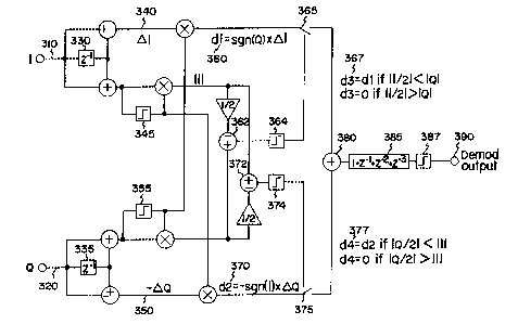
Fig. 3 illustrates in greater detail the architecture of the FM demodulator
used
in a transceiver system. The in-phase signal 310 and the quadrature signal 320
are
routed through a time sampling detector for a binary frequency shift key
modulated
input signal, wherein a discrete-time period rather than a continuous time
period is
used. The in-phase baseband signal 310 and the quadrature baseband signal 320
have been oversampled by a predetermined factor with respect to the data rate.
Those skilled in the art understand that the oversampling factor above is not
limited
to a finite number. The demodulator differentiates the in-phase signal 310 by
computing the difference between the current value of the in-phase signal 310
and
the value of the signal delayed by one clock cycle 330. The result is a
differentiated
in-phase signal (0I) 340.
Further, the demodulator differentiates the quadrature signal 320 by
computing the difference between the current negative value of the quadrature
signal
320 and the value of the signal delayed by one clock cycle 335. The result is
a
differentiated quadrature signal (-OQ) 350. The sign of the differentiated in-
phase
signal 340 and differentiated quadrature signal 350 is modified depending on
the
sign of the quadrature signal 355 and the in-phase signal 345, respectively.
The
resulting modified differentiated in-phase signal and modified differentiated
quadrature signal create dl 360 and d2 370, respectively.
Mathematical, this may be represented by Equation [1] and Equation [2],
respectively. This change in the polarity of the differentiated signals
insures that the
subsequent addition of dl 360 and d2 370 results in a proper output. To reduce
the
sensitivity to noise in the in-phase signal 310 and the quadrature signal 320,
a
CA 02365689 2001-08-29
WO 00/52818 PCT/US00/05184
6
comparison 364, 374 between the amplitude of in-phase signal 362 and the -
amplitude of the quadrature signal 372 is performed and the smaller of the
modified
differentiated in-phase or quadrature signal is discarded. This switching for
the
selection function is represented by 367, 377:
d3 = dl if ~I/2 ~ < ~Q ~ [3]
or
d3 = 0 if ~I/2 ~ > ~Q ~ [4]
and
d4 = d2 if ~Q/2 ~ < ~I ~ [5]
or
d4 = d2 if ~Q/2 ~ > ~I ~ [6]
The resulting signals are added 380, then the signal is low pass filtered 385
by a 4-
tap delay line and then sliced by a comparator 387 to recover the transmitted
bit.
Digital data 390 is produced as an output of the demodulator .
Fig. 4 is a diagrammatic representation of a signal constellation. To achieve
higher bit rates in a fixed spectrum bandwidth, multilevel modulation and
demodulation schemes are used. The four-level, or quadrature implementations
are
used to provide bandwidth efficiency and low bit energy to noise energy ratio
requirement for error probability performance. The complex signal can be drawn
using an in-phase (I) 410 and a quadrature (Q) 420 branch representing the
orthogonal cosine and sine terms in the transmitted signal. The mapping of the
two
possible states is represented by the direction of rotation around the signal
constellation 400, clockwise or counterclockwise. The implementation of the
signal
constellation reduces the sensitivity to noise in the in-phase and the
quadrature input
signals. The reduction of noise sensitivity in the in-phase and the quadrature
signals
is accomplished by comparing the amplitude of an in-phase input channel to a
quadrature input channel. The differentiated lower amplitude signal is
discarded
rather than summed with the higher amplitude channel. A function of the signal
constellation comprises ensuring that the subsequent addition of dl 430 and d2
440
result in a positive output if a signal constellation 400 has rotated
clockwise, and in a
negative output if the signal constellation 400 has rotated counterclockwise,
regardless of the quadrant in which the constellation happens to be in.
Mathematically, this is how the signal constellation chooses:
CA 02365689 2001-08-29
WO 00/52818 PCT/US00/05184
7
dl if ~I/2 ~ < ~Q ~
d2 if ~Q/2 ~ < ~I ~ (8~
dl + d2 otherwise
Note that the absolute value of the in-phase (I) and the quadrature (Q) signal
divided
by two, in equations 3 through 9, is approximately equal to multiplying the
result of
the absolute value of the in-phase (I) and the quadrature (Q) signal by the
tan(~/7).
The value, ~/7, is shown in Fig. 4 as the signal constellation's rotational
interval.
Fig. 5 is a flow diagram illustrating method of performing FM demodulation
according to the present invention. The in-phase S00 and the quadrature 510
signals
enter the demodulator as baseband signals. The difference between the current
value
of the in-phase signal 500 and the value of the in-phase signal delayed by one
clock cycle is calculated and the result is a differentiated in-phase signal (
~~I) 520.
The difference between the current value of the quadrature signal 510 and the
value
of the quadrature signal delayed by one clock cycle is calculated and the
result is a
differentiated quadrature signal (~OQ) 530. After multiplying the sign of the
quadrature signal with differentiated in-phase signal (DI) 540 and the sign of
the in-
phase signal with the negative of the differentiated quadrature signal (-0Q)
550, a
decision is made as to what value of the in-phase and the quadrature signal
571,
572, 573, 574 will be added together 575 to produce a non-filtered output
signal.
This signal is passed through a filter 580 and sliced by a comparator to
recover the
data in a digital form 590.
Fig. 6 is a digital representation of an FM demodulator circuit. The in-phase
signal 600 and the quadrature 610 input signals are routed through an in-phase
analog-to-digital converter 620 and a quadrature analog-to-digital converter
630,
respectively. The digital forms of the in-phase and quadrature signals are
routed to
a binary frequency shift key (BFSK) circuit 640. Those skilled in the art will
understand that the binary frequency shift key circuitry 640 can include a
digital
signal processor (DSP) which implements the functionality similar to Fig. 2
and Fig.
3. The output of the binary frequency shift key circuitry 640 is an analog
waveform
650.
In summary, the FM demodulator circuit architecture according to the present
invention provides reduced sensitivity to noise and enhances the performance
of a
system with that of the theoretical predictions for an ideal demodulator.
The foregoing description of the exemplary embodiment of the invention has
been presented for the purposes of illustration and description. It is not
intended to
CA 02365689 2001-08-29
WO 00/52818 PCT/US00/05184
8
be exhaustive or to limit the invention to the precise form disclosed. Many -
modifications and variations are possible in light of the above teaching. It
is
intended that the scope of the invention be limited not with this detailed
description,
but rather by the claims appended hereto.