Note: Descriptions are shown in the official language in which they were submitted.
CA 02365952 2001-12-17
P1650
TITLE OF THE INVENTION
sEMICONDUCTOR LASER DEVICE FOR UsE IN A SEMICONDUCTOR LASER
MODULE AND OPTICAL AMPLIFIER
BACKGROUND OF THE INVENTION
FIELD OF THE INVENTION
The present invention relates to a semiconductor laser module, and an optical
amplifier using the
semiconductor laser module, and ~onore particularly to a semiconductor laser
device provided with two
stripes from which two laser beams arc emitted, and an optical amplifier.
DISCUSSION OF TIC BACKGROUND
With progress is optical com~riu~aications based on a high-density wavelength
division
multiplexing transmission system over the recent years, a higher output is
inczeasingly Qemaxtded to a
pumping light source used for the optical amplifier.
Further, a Beater expectation is recently given to aRamaa amplifier as moans
fot amplifying
the beams having R much broader band than by as erbium-doped optical amplifier
that has hitherto been
used as the optical amplifier. 'Ibe Rat~aan amplification is defined as a
method of amplifying the optical
signals, which utilizes such, a phenomenon that a gain occurs on the side of
frequencies as low as about 13
THz from a pumping beam wavelength due to the stimulatman scattering occurred
when the
pumping beams enter an optical fiber, and, when signal beams having the
wavelength band containing the
gain described above are inputted to the optical fiber in the thus pumped
(excaited) state, these signal beams
are amplified.
According to tb~eRanaan atxtplifxcation, the signal beams are amplified in a
state where a
polarising direction of the signal beams is coincident with a polari2ing
direction of the pumping beams,
and it is therefore required that an influents caused by a deviation between
polatizillg planes of the signal
beam and of the pumping beam be minimized. For attaining this, a dcgrcc of
polarization (DOP) has
hitherto been reduced by obviating the polarization of the pumping beam
(depolarization).
CA 02365952 2001-12-17
As a method for simultaneously realizing a higher output and depolarization of
a
pumping light source, as disclosed in US Patent No. 5589684, a method in which
a laser
beam emitted from two semiconductor laser modules oscillating on the same
wavelength is
polarization-synthesized by a polarization synthesizing coupler is known.
Fig. 35 is an explanatory view in explaining a conventional semiconductor
laser
apparatus disclosed in US Patent No. 5589684.
As shown in Fig. 35, a conventional semiconductor laser apparatus comprises: a
first semiconductor laser device 100 and a second semiconductor laser device
101 for
emitting laser beams in the orthogonal direction with each other on the same
wavelength; a
first collimationlens 102 for collimating the laser beam emitted from the
first semiconductor
laser device 100; a secondcollimationlens 103 for collimating the laser beam
emitted from
the second semiconductor laser device 101; a polarization synthesizing coupler
104 for
orthogonally polarization-synthesizing the laser beam collimated by the
first;ollimation lens
102 and the second collimation lens 103; a condenser lens 105 for condensing
the laser
beams polarization-synthesized by the polarization synthesizing coupler 104;
and an optical
fiber 107 with a fiberBragg grating (FBG) 106 for receiving the laser beams
condensed by
the condenser lens 105 and letting the beams travel to the outside.
According to a conventional semiconductor laser apparatus, since the laser
beams
emitted in the orthogonal direction with each other from the first
semiconductor laser device
100 and the second semiconductor laser device 101 are polarization-synthesized
by the
polarization synthesizing coupler 104, a laser beam whose degree of
polarization is small can
be emitted from the optical fiber 107. Furthermore, since fiberBragg grating
106 is formed
in the optical fiber 107, oscillation wavelengths of the semiconductor laser
devices 100 and
101 are fixed in the same degree, a laser beam whose wavelength is fixed can
be emitted
from the optical fiber 107.
Accordingly, the above-mentioned conventional semiconductor laser apparatus
can
be applied as a pumping light source of an opticalamplifier which requires a
high optical
output, especially of a Raman amplifier, which requires a low polarization
dependency and a
wavelength stability.
A conventional semiconductor laser apparatus has the following problems.
CA 02365952 2001-12-17
(1) In the conventional semiconductor laser apparatus, two chip carriers with
two
semiconductor laser devices 100 and 101 attached thereto respectively need to
be disposed on
a base plate by soldering. At this time, since positioning need to be
conducted so that laser
beams emitted from the two semiconductor laser devices 100 and 101 be
orthogonal with
each other, it is difficult to conduct the positioning of the semiconductor
laser devices and a
time for positioning becomes longer. As a result, a time for manufacturing a
semiconductor
laser module is increased.
(2) Since the beams emitted from each of the semiconductor laser devices 100
and
101 are emitted in completely different directions from each other, there
arises, for example,
a warp of a package in which optical components are aligned and fixed under a
state of a high
temperature. Due to this, it is difficult to stabilize beam intensity and a
degree of
polarization of the beam emitted from the optical fiber.
(3) In the conventional semiconductor laser apparatus, sincecollimation lenses
102
and 103 for collimating the laser beams emitted from the semiconductor laser
device 100 are
used, a beam diameter and an image magnification are enlarged. Therefore,
there is a
problem in that a tolerance for the position and angle is strict.
(4) In order to cool the two semiconductor laser devices 100 and 101
positioned at a
space, a large-sized Peltier module is required. As a result, there is a
problem
in that the electric power consumption of a semiconductor laser module is
increased.
(5) In the conventional semiconductor laser apparatus, an optical fiber with
the fiber
Bragg grating 106 and the semiconductor laser devices 100 and 101 need to be
optically
coupled. Since the optical coupling includes mechanically connected portions
to forma
resonator, there is a fear that an oscillation characteristic of the laser
beam is changed due to a
mechanical vibrationor a change in temperature. Therefore, there is a problem
in that it is
impossible to provide a stable optical output in some cases.
(6) Wavelengths of the laser beams emitted from each of the semiconductor
laser
devices 100 and 101 are determined by asingle FBG and thus it is impossible to
separately
set the wavelength of each semiconductor laser device
Furthermore, if this semiconductor laser device isused as a pumping light
source for
the Raman amplification, there are the following problems.
CA 02365952 2001-12-17
(7) In the conventional semiconductor laser device,the_resonance between the
fiber
Bragg grating 106 and an optical reflection surface (rear edge surface of the
semiconductor
laser devices) creates noise peaks that appear periodically on thefreaquency
axis of the
relativie intensity (RIN) profile. These peaks function to add noise to
amplified signals, since
amplification occurs at an early stage in theRaman amplification,where the
fluctuation in
pumping beam intensityis transposed to that in a Raman gain. Therefore, there
is a problem
in that a stable Raman amplification can not be conducted.
(8) As an optical amplification method,there is a backward pumping in which a
pumping beam is supplied in the opposite direction of the traveling direction
of the signal
beam, a forward pumping in which a pumping beam is supplied in the same
direction of the
traveling direction of the signal beam and abidirectional pumping in which
pumpin~eams
are supplied in both of the directions At present, however, only the backward
pumping is
mainly usedin the Raman amplified because in the forward pumping a weak signal
beam
propagates together with a intense pumping beam in the same direction,making
the
fluctuation of the pumping beam intensitymore likely to be transposed to that
of the
amplified signal beamthan backward pumping Therefore, there is a demand for a
stable
pumping lightsource which can be applied to the forward pumping. In other
words, the
semiconductor laser module using a conventional fiberBragg grading has a
problem in that
applicable pumping methods are limited.
(9) In the Raman amplification,the amplification can take place wheathe
polarizing
direction of the signal beams is coincident with the polarizing direction of
the pumping
beams. That is, in the Raman amplification, there is a polarization dependency
of an
amplification gain, and an influence due.to a deviation between the polarizing
direction of the
signal beam and the polarizing direction of the pumping beam should be
minimized. Here,
in the case of the backward_pumping, since polarizationof the pumping beam is
randomized
while propagating in the fiber in the opposite direction to the signal beam,
there arisesless
problem. However, in the case of the forward pumping, polarization dependency
is strong
and thus the polarization dependency needs to be reduced by orthogonal
polarization
synthesizing of the pumping beak depolarization and the like.
CA 02365952 2001-12-17
In other words, a degree of polarization (DOP) of the pumping beam needs to be
minimized. Furthermore, since inRaman amplification, thegain is relatively
low, a
pumping light source for the Raman amplification having a high output has been
demanded.
In contrast to the prior art, the embodiments of the present inventio~re for a
semiconductor laser
module, a manufacturing method thereof and an optical amplifier that are
capable of obtaining a high
optical coupling efficiency, attaining a down-size and a mass-production, and
reducing both of a
manufacturing time and a manufacturing cost.
The present invention provides a semiconductor laser device having a plurality
of stripes formed
at a space, wherein laser beams are emitted from one-sided edge surfaces of
the respective stripes and
diffraction gratings are provided in the respective stripes.
In particular, the present invention provides asemiconductor laser
devicecomprising a first light
emitting stripe aligned to emit a first laser beam through one edge surface
and at least one othetight
emitting stripe aligned to emit at least one other laser beam through the one
edge surfa~euvhereinthe first
light emittingstripe aligned to emit the first laser beam through the one edge
surface and an opposite edge
surface and the least one otherlight emittingstripe aligned to emit at the
least one other laser beam through
the one edge surface and the opposite edge surface
A more complete appreciation of the invention and many of the attendant
advantages
thereof will be readily obtained as the same becomes better understood by
reference to the
following detailed description when considered in connection with the
accompanying
drawings, wherein:
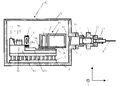
FIG. 1(A) is a side sectional view showing a configuration of a semiconductor
laser
module in accordance with a first embodiment of the present invention; FIG.
1(B) is a side
view showing a state where a semiconductor laser device is fixed onto a heat
sink;
FIG. 2 is an explanatory diagram schematically showing a configuration of the
semiconductor laser module in accordance with the first embodiment of the
present
invention;.
CA 02365952 2001-12-17
FIG. 3(A) is a side view showing a configuration of a prism; FIG. 3(B) is a
plan view
thereof;
FIG. 4(A) is a plan view showing apolarization synthesizing module; FIG. 4(B)
is a
side sectional view thereof; FIG. 4(C) is a front view thereof;
FIG. S is a graph showing a spectrum when a drive current 2A (1A applied per
stripe)
is applied in a double-stripe type semiconductor laser module;
FIG. 6 is a graph showing a fiber output versus an LD drive current in the
double-
stripe type semiconductor laser module;
FIGS. 7(A) and 7(B) are explanatory diagrams showing a step of aligning a
first lend
FIGS. 8(A) to 8(C) are explanatory views showing a configuration of the
semiconductor laser device; FIGS. 8(B) and 8(C) are sectional views each taken
along the
line a-a in FIG. 8(A);
FIG. 9 is an explanatory view showing another example of the semiconductor
laser
device;
FIG. 10 is an explanatory diagram schematically showing a configuration of the
semiconductor laser module in accordance with a second embodiment of the
present
invention;
FIG.11 is an explanatory diagram schematically showing a configuration of the
semiconductor laser module in accordance with a third embodiment of the
present invention
FIG. 12 is a fragmentary perspective view showing apolarization synthesizing
module in accordance with a fourth embodiment of the present invention;
FIG. 13 is a side sectional view showing thepolarization synthesizing module
shown
in FIG 12;
FIG.14 is an explanatory diagram schematically showing a semiconductor laser
device in accordance with the fifth embodiment of the present invention
FIGS.15(A) to 15(C) are explanatory views showing a configuration of the
semiconductor laser device in accordance with a sixth embodiment of the
present invention;
FIGS.15(B) and 15(C) are a sectional view taken along the line b-b in
FIG.15(A) and a
sectional view taken along the line c-c in FIG. 15(A), respectively;
FIG. 16 is a graph showing a relationship between an oscillation spectrum and
oscillation longitudinal mode in the semiconductor laser device in accordance
with the sixth
CA 02365952 2001-12-17
embodiment of the present invention;
FIGS. 17(A) and (B) are graphs showing a relationship in laser optical output
power
between a single oscillation longitudinal mode and a plurality of oscillation
longitudinal
modes, and a threshold value of stimulatedBrillouin scattering;
FIGS. 18(A) to 18(C) are vertical sectional views each showing in the
longitudinal
direction a configuration of the semiconductor laser device in accordance.
with a seventh
embodiment of the present invention;
FIG.19 is a vertical sectional view showing in the longitudinal direction a
configuration of the semiconductor laser device in accordance with an eighth
embodiment of
the present invention;
FIG. 20 is an explanatory diagram showing a fluctuation in period of
diffraction
gratings provided in the semiconductor laser device shown in FIG. 1~
FIG. 21 is an explanatory diagram showing a modified example for actualizing
the
fluctuation in period of the diffraction gratings provided in the
semiconductor laser device
shown in FIG. 19;
FIG. 22 is an explanatory diagram schematically showing a configuration of the
semiconductor laser module in accordance with an eleventh embodiment of the
present
invention;
FIG. 23 is an explanatory diagram schematically showing a configuration of the
semiconductor laser module in accordance with a twelfth embodiment of the
present
invention;
FIG. 24 is an explanatory diagram schematically showing a configuration of the
semiconductor laser module in accordance with a thirteenth embodiment of the
present
invention;
FIG. 25 is an explanatory diagram schematically showing a configuration of the
semiconductor laser module in accordance with a fourteenth embodiment of the
present
invention;
FIG. 26 is an explanatory diagram showing an example of a photo diode (light
receiving element) in accordance with a fifteenth embodiment of the present
invention
FIG. 27 is an explanatory diagram schematically showing a configuration of the
semiconductor laser module in accordance with a sixteenth embodiment of the
present
CA 02365952 2001-12-17
invention;
FIG. 28 is a graph showing a beam transmissivity when entering a wavelength
selection filter 7~
FIG. 29 is an explanatory diagram schematically showing a configuration of the
semiconductor laser module in accordance with a seventeenth embodiment of the
present
invention;
FIG. 30 is~an explanatory diagram showing a wedge-shaped prisrtl
FIG. 31 is an explanatory diagram showings optical path correction prism;
FIG. 32 is an explanatory diagram showing coupling ofGaussian beams
FIG. 33 is a block diagram showing a configuration of aRaman amplifier in
accordance with a eighteenth embodiment of the present invention;
FIG. 34 is a block diagram showingan architecture of a WDM communication
system
to which the Raman amplifier shown in FIG. 33 is applied.
FIG.35 is a explanatory diagram showing a semiconductor laser module as
disclosed
in USP5,589,684.
CA 02365952 2001-12-17
Embodiments of the present invention will hereinafter be described with
reference to
the accompanying drawings.
(First Embodiment)
FIG. 1(A) is a side~sectional view showing a configuration of the
semiconductor laser
module in accordance with a first embodiment of the present invention. FIG. 2
is an
explanatory diagram schematically showing the configuration of the
semiconductor laser
module in accordance with the first embodiment of the present invention.
As shown in FIG. 1(A), a semiconductor laser module Ml in accordance with the
first
embodiment of the present invention includes a package 1 of which an interior
is hermetically
sealed, a semiconductor laser device 2, encased in the package 1, for emitting
laser beams, a
photo diode (a light receiving element) 3, a first lens 4, a prism 5, a half
wave plate (a
polarization rotating element) 6, a PBC (polarization beamcombiner) 7 serving
as an optical
synthesizing element and an optical fiber 8.
The semiconductor laser device 2 includes, as shown in FIG. 2, a first stripe
9 (a
stripe-shaped light emitting portion) and a second stripe 10 disposed with an
interval on the
same plane and extending in parallel in the longitudinal direction. The
semiconductor laser
device 2 emits a first laser beam Kl and a second laser beam K2 respectively
from edge
surfaces of the first and second stripes 9, 10. K1 and K2 shown in FIG. 2
represent
trajectories of the centers of the beams that exit the first and second
stripes 9, 10, respectively.
The beam travels, as indicated by a broken line in FIG. 2, with some
divergence (spread)
about the center thereof. A space between the first stripe 9 and the second
stripe 10 is set as
100 wm or less e.g., approximately 40-60 p.m in order for the beams Kl, K2
exiting these
stripes 9, 10 to enter one piece of first lens 4. Moreover, the space between
the stripes is
narrow, whereby a difference in optical output characteristic between the
stripes decreases.
As shown in FIG. 1(A), the semiconductor laser device 2 is fixedly fitted onto
a chip
carrier 11. Note that the semiconductor laser device 2 emits the two laser
beams Kl, K2 and
is therefore easier to become exothermic than a semiconductor laser device for
emitting the
single laser beam. It is therefore preferable that the semiconductor laser
device 2 be fixedly
fitted onto a heat sink 58 composed of a material exhibiting a high thermal
conductivity such
CA 02365952 2001-12-17
as diamond and so forth, and that the heat sink 58 be fixedly fitted onto the
chip carrier 11.
The photo diode 3 receives a monitor-oriented laser beam emitted from a rear
(left
side in FIG. 1(A)) edge surface 2b (see FIG. 2) of the semiconductor laser
device 2. The
photo diode 3 is fixedly attached to a photo diode carrier 12.
The first and second laser beams Kl, K2 exiting a front (right side in FIG.
1(A)) edge
surface 2a of the semiconductor laser device 2 are incident upon the first
lens 4 The first
lens 4 functions so that these laser beams Kl, K2 traveltherethrough and
intersect each other
to subsequently split and expand in the arrayed direction of the stripes 9 and
10, and focuses
these beams at different focal position Fl, F2, respectively(see FIG. 2).
Normally, parallel beams transformed into a large spot size have an angular
tolerance
that is as strict as 0.1° or smaller, however, the angular tolerance
slackens in the condensing
optical system which converges the laser beams at focal positions Fl, F2 as
described above.
Since the first lens 4 is disposed as a condensing optical system in this
embodiment, a
manufacturing and positioning tolerance of the optical elements, as well as an
angular
adjusting tolerance of a beam are slack. This is a preferable aspect.
As shown in FIG. 1(A), the first lens 4 is held by a first lens holding member
13. As
shown in FIG. 2, the first lens 4 is preferably positioned so that the optical
axis of the first
laser beam Kl emerging from the first stripe 9 and the optical axis of the
second laser beam
K2 emerging from the second stripe 10 show substantially a symmetry about the
central axis
of the first lens 4. With this arrangement, both of the first and second laser
beams Kl, K2
travel through the vicinity of the central axis of the first lens 4 that is
defined as an area with
a small aberration, and hence there is a decreased scatter on the wave
surfaces of the laser
beams, with the result that the optical coupling efficiency to the optical
fiber 8 rises. As a
result, a higher optical output may be obtained from the semiconductor laser
module Ml.
Note that the first lens 4 preferably involves the use of an aspherical lens
exhibiting a small
spherical aberration for a high coupling efficiency to the optical fiber to be
obtained.
The prism 5 is disposed between the first lens 4 and the PBC 7 and adjusts the
~tical
paths, substantially collimates the optical axes, of the first and second
laser beams Kl, K2,
thus letting the laser beams Kl, K2 exit the prism S itself. The prism 5 is
composed of an
optical glass of BK7 (borosilicate crown glass) and so on. The optical axes of
the first and
second laser beams Kl, K2 traveling in non-parallel from the first lens 4 are
collimated by
CA 02365952 2001-12-17
refraction of the prism 5, and hence the forming of the PBC 7 disposed in rear
of the prism S
is facilitated and it becomes feasible to downsize the semiconductor laser
module Mby
downsizing the PBC 7.
FIG. 3(A) is a side view showing a configuration of the prism 5, and FIG. 3(B)
is a
plan view thereof. In FIGS. 3(A) and 3(B), the prism 5 includes an incident
surface5a
formed flat and exit surfaces Sb inclined at a predetermined angle a . For
example, the prism
may be formed of BK7, the entire length Ll thereof may be approximately l.Omm,
and cr
may be designed to be 3.~ ~ 0.1 °, for the case of the stripes being
spaced by 40,u m, and the
focal length of the first lens being chosen to be 0.7mm.
As shown in FIG. 2, the half-wave plate 6 admits an incidence of only the
first laser
beam Kl of the first and second laser beams Kl, K2 passing through the prism
5, and rotates
by 90 degrees a polarizing surface of the first laser beam Kl incident
thereupon. The first
lens 4 splits the first and second laser beams Kl, K2 widely enough folthe
half wave plate 6
to be able to be disposed easily.
The PBC 7 has a first input part 7a on which the first laser beam Kl is
incident, a
second input part 7b on which the second laser beam K2 is incident, and an
output part 7c
where the first laser beam entering the first input part 7a and the second
laser beam K2
entering the second input part 7b are multiplexed (synthesized) and thus exit.
The PBC 7
may be, for instance, a birefringence element through which the first laser
beam Kl travels as
an ordinary ray to the output part 7C and the second laser beam K2 travels as
an
extraordinary ray to the output part 7c. The PBC 7, if being the birefringence
element, may
be composed of, e.g., rutile (Ti02) to obtain a high index of birefringence
and a large split
width between the laser beams.
In the first embodiment, apolarization synthesizing module 59 is adopted in
which
the prism 5, the half-wave plate 6 and the PBC 7 are fixed to the same holder
member 14.
FIG. 4(A) is a plan view showing thepolarization synthesizing module 59. FIG.
4(B) is a
side sectional view thereof. FIG. 4(C) is a front view thereof. As shown in
FIGS. 4(A) to
4(C), the holder member 14 of the polarization synthesizing module 59 is
composed of a
material (for example, SUS403, SUS304 and so on) suitable for YAG laser
welding. The
holder member 14 is approximately 7.0 mm in its entire length L2 and is formed
substantially
CA 02365952 2001-12-17
in a cylindrical shape as a whole. The holder member 14 is formed inside
wit>:n
rectanguler accommodation space 14a in which the prism S, the half-wave plate
6 and the
PBC 7 are fixedly provided, respectively. The holder member 14 is opened at
its upper
portion and is flat in its lower portion.
This configuration greatly facilitates adjusting the positions of the prism 5
and the
PBC 7 about a central axis Cl so that both of the first laser beam Kl incident
upon the first
input part 7a of the PBC 7 and the second laser beam K2 incident upon the
second input part
7b thereof, exit the output part 7c.
Thus, these optical elements are set integral within the holder member 14, and
it is
therefore possible to adjust a degree of how much the laser beams Kl, K2
overlap with each
other on the X-Y plane simply by moving the holder member 14.
As shown in FIG. 2, the optical fiber 8 receives the laser beams exiting the
output part
7c of the PBC 7 and lets the laser beams travel outside the package 1. The
optical fiber 8 is,
as shown in FIG. 2, provided with a beam reflection element 15 consisting of
an FBG (fiber
bragg grating) that reflects the beams having a predetermined wavelength
range. This beam
reflection element 15 reflects the beams having the predetermined wavelength
back to the
semiconductor laser device 2. With this beam reflection element 15, an
oscillation
wavelength of the semiconductor laser device 2 is fixed, and an oscillation
spectral width can
be decreased. Accordingly, the laser beams emitted from the semiconductor
laser modules
Ml can be multiplexed with decreased loss at wavelength synthesizing coupler,
and therefore,
high output, multiplexed beams can be obtained which is suitable for use as a
pumping light
source of an erbium doped optical amplifier or aRaman amplifier If used for a
Raman
amplifier, a fluctuation in gain of theRaman amplification can be restrained.
The beam
reflection element 15 is formed by irradiating a core of the optical fiber 8
with ultraviolet rays
serving as interference fringes through, e.g., a phase mask, and consequently
causing periodic
changes in refractive index.
A second lens 16 for optically couplingthe laser beams emerging from the
output part
7c of the PBC 7 to the optical fiber 8, is disposed between the PBC 7 and the
optical fiber 8.
Preferably, the first lens 4 is positioned so that the first and second laser
beams Kl, K2 are
focused on points (Fl, F2) between the first lens 4 and the second lens 16.
With this
contrivance, a propagation distance L needed for the first and second laser
beams Kl, K2 to
12
CA 02365952 2001-12-17
split widelyenough for a half wave plate 6 to be able to be inserted only on
the beam path of
Kl (in other words, for a distance D' in FIG. 2 to take a sufficiently large
value)is increased,
because of the reduced beam spot sizes between the first lens 4 and focal
points (Fl, F2)
which reduces overlapping of the two laser beams. Hence a length of the
semiconductor laser
module Ml in the optical-axis direction can be reduced. As a result, it is
feasible to
provide the highly reliable semiconductor laser module M1 exhibiting an
excellent stability
over time of the optical coupling of the semiconductor laser device 2 to the
optical fiber 8
under, e.g., a high-temperature environment.
As shown in FIG. 1, the chip carrier 11 to which the semiconductor laser
device 2 is
fixed and the photodiode carrier 12 to which the photo diode 3 is fixed, are
fixed by soldering
onto a first base plate 17 taking substantially an L-shape in section. It is
preferable that the
first base plate 17 be composed of a CuW based alloy and so on in order to
enhance a
capacity of transferring the heat evolved by the semiconductor laser device 2.
The first len~.holding member 13 to which the first lens 4 is fixed and the
polarization
synthesizing module 59 with the prism 5, the half-wave plate 6 and the PBC 7
fixed to the
holder member 14, are fixed by the YAG laser welding onto a second base plate
18 through a
first support member 19a and a second support member 19b, respectively. It is
therefore
preferable that the second base plate 18 be formed of a stainless steeletc
showing a high
welding property. Further, the second base plate 18 is fixed bybrazing onto a
flat part 17a
of the first base plate 17.
A cooling device (thermo-electric cooler) 20 constructed of a plurarity of
Peltier
elements are provided under the first base plate 17. Athermistor 20a provided
on the chip
carnet 11 detects a change in temperature due to the heat transferred from the
semiconductor
laser device 2. The cooling device 20 is controlled to keep constant the
temperature
detected by the thermistor 20a. This contrivance makes it feasible to increase
and stabilize
the output of emission of the laser beams from the semiconductor laser device
2.
A window 1b upon which the beams penetrating the PBC 7 are incident is
provided
inside the flange la formed at the side area of the package 1, and a second
lens 16 for
converging the laser beams is fixed at the end of the flange la. The second
lens 16 is held
by a second lens holding member 21 fixed by the YAG laser welding to a side
edge of the
flange la. A metallic slide ring 22 is fixed by the YAG laser welding to a
side edge of the
13
CA 02365952 2001-12-17
second lens holding member 21.
The optical fiber 8 is held by a ferrule 23 fixed by the YAG laser welding to
an
interior of the slide ring 22.
Next, operations of the semiconductor laser module M1 in accordance with the
first
embodiment of the present invention will be explained.
As shown in FIG. 2, the first and second laser beams Kl, K2 emitted from the
front
edge surfaces 2a of the first and second stripes 9, 10 of the semiconductor
laser device2,
penetrate the first lens 4 and intersect each other. Thereafter, the laser
beams Kl, K2 having
a sufficient divergence split thoroughly and thenenter the prism 5. A width of
divergence
(D) between the first and second laser beams Kl, K2 when entering the prism S
is
approximately 460,um. The first and second laser beams Kl, K2 are collimated
by the prism
and thus exit (the width of divergence between the laser beams Kl and K2
becomes
approximately SOO,u m at the exit). Then, the first laser beam K1 impinges on
the half wave
plate 6 and, after its polarization plane has been rotated by 90 degrees,
enters the first input
part 7a of the PBC 7, while the second laser beam K2 enters the second input
part 7b of the
PBC 7.
In the PBC 7, the first laser beam Kl emerging from the first input part 7a
and the
second laser beam K2 emerging from the second input part 7b, are multiplexed
and exit the
output part 7c.
The laser beams emitted from the PBC 7 are converged by the second lens 16,
then
incident upon the edge surface of the optical fiber 8 held by the ferrule 23,
and propagate
outside. Further, some proportion of the laser beams are reflected by the beam
reflection
element 15 of the optical fiber 8 back to the semiconductor laser device 2,
thereby forming an
external resonator between the rear edge surface 2b ol;.the semiconductor
laser device 2 and
the beam reflection element 15. Hence, the laser oscillations with a
wavelength determined
by the beam reflection element 15 can occur.
The monitor-oriented laser beams emerging from the rear edge surface 2b of the
semiconductor laser device 2, are received by the photo diode 3. An optical
output or the
like of the semiconductor laser device 2 is adjusted by changing the driving
current applied to
the semiconductor laser device 2 based on a light receiving quantity etc. of
the photo diode 3.
14
CA 02365952 2001-12-17
According to the semiconductor laser module M1 in accordance with the first
embodiment of the present invention, the first and second laser beams Kl, K2
with their
polarization planes coincident with each other are emitted from the first and
second stripes 9,
formed at the space as narrow as 100 wm or less in the single semiconductor
laser device 2.
The first and second laser beams Kl, K2 are thoroughly split from each other
by the first lens
4, and thereafter the polarization plane of the first beam isrotated exactly
by 90 degrees with
the half-wave plate 6. Namely, the polarization planes of the laser beams Kl,
K2 make
substantially completely 9~ at this time. The first and second laser beams Kl,
K2 are
polarization-synthesized by the PBC 7in this state, and hence the laser beams
having the high
output and a small degree of polarization can be emitted out of the optical
fiber 8. Further,
the optical fiber 8 is formed with~beam reflection element l5such as FBG, and
therefore
the laser beams with a fixed wavelength can be emitted out of the optical
fiber 8. Accordingly,
the semiconductor laser module Ml can be applied for the pumping light source
foran
erbium-doped optical amplifier of whicha high output is demanded or for a
Raman amplifier
which is required to have a low polarization dependency of gain and a high
gain stability.
Further, since the semiconductor laser module Ml uses one piece
ofsemiconductor
laser device 2 formed with two stripes for emitting two fluxes of laser beams
and one piece of
first lens 4 for splitting the two laser beams, it takes less time to position
the semiconductor
laser device 2 and the first lens 4. As a result, it is possible to reduce the
time for
manufacturing the semiconductor laser module M1.
Moreover, there has hitherto been the semiconductor laser module as disclosed
in
USP5,589,684, in which two pieces of semiconductor lasers emit the laser beams
in the axial
directions completely orthogonal to each other (refer to FIG.35). This type of
semiconductor laser module is, however, if designed without taking a warp or
the like of the
package in the axial directions(a X direction and a Z direction in FIG.35)
into account,
incapable of restraining fluctuations in the optical output due to the warp of
the package that
arises in high temperature environment.By contrast, according to the
configuration in the
first embodiment, the two laser beams emitted from the single semiconductor
laser device 2
travel substantially in the same direction, and hence the optical output of
the laser beams
emerging from the optical fiber 8 can be stabilized by restraining an
influence of the warp of
the package only in one direction (a Z-direction in FIG. 2).
CA 02365952 2001-12-17
Further, the single semiconductor laser device 2 emits the two laser beams,
and the
coupling efficiencies of these two laser beams have the same tendency of
fluctuations with
respect to the package warp and so on. Accordingly, the degree of polarization
of the laser
beams emitted from the optical fiber 8 isstable over the temperature
fluctuation.
Further, since the semiconductor laser module Ml uses a single semiconductor
laser
device 2, it is possible to.downsize the cooling device 20(e.g. a Peltier
module) and to
decrease the of electric power consumption.
Note that the electric power consumed when the cooling device 20 radiates a
tremendous quantity of heat from the two stripes 9, 10 can be reduced to a
large extent by
creating a vacuum or fillingXe in the interior of the package 1.
Moreover, if a polarization maintainingfiber formed with the fiberBragg
grating
(FBG) is attached to the semiconductor laser module emitting the two fluxes of
laser beams
("double-stripe type semiconductor laser moduld') as in the first embodiment,
more
longitudinal modes can be contained within the spectral width than in the case
o~he single-
stripe type semiconductor laser module emitting one flux of laser beam with
the same
magnitude of reflection bandwidth of FBG.
Foe instance, FIG. 5 is a graph showing an oscillation spectrum when applying
a drive
current of 2A (1A per stripe) to the double-stripe type semiconductor laser
module M1. As
can be understood from FIG. 5, five longitudinal modes are contained within
the full width at
half maximum (FWHM~f the spectrum of the double-stripe type semiconductor
laser
module Ml. On the other hand, in the case of a single-stripe type
semiconductor laser
module, three or four longitudinal modes are contained within the FWHMof the
oscillation
spectrum at the drive current 1A.
Since the polarization maintainingfiber has a refractive index that differs
depending
on a slow-axis and a fast-axis, the reflection wavelengths selected in the two
axes at the FBG
differ from each other by about 0.4 nm. Hence, the spectrums from the two
stripes, each
emitting a spectrum different from the other by about 0.4nm, overlap to
contain an increased
number of longitudinal modes within the FWHM of the synthesized spectrum.
Note here that the semiconductor laser module according to this embodiment of
the
present invention emits a polarization-synthesized laser beam witHower DOP
than laser
beam from a single stripe. In case, however,that DOP is not sufficiently
reduced a output
16
CA 02365952 2001-12-17
beam might be further depolarized by being transmitted through a length of
apolarization
maintaining fiber ~lepolarizer). Then, since the semiconductor laser module
according to this
embodiment oscillates in an increased number of longitudinal modes, the DOP
can be
effectively reducedwhile propagating through the depolarizer. Therefore the
semiconductor
laser module M1 is suitable as the pumping light source otRaman amplifiers
which are
required to have the low polarization dependency of gain
Further, the double-stripe type semiconductor laser module is capable of
obtaining
high optical output. FIG. 6 is a graph showing a fiber output versus a drive
current to the
semiconductor laser device in the double-stripe type semiconductor laser
module. As can be
understood from FIG. 6, an eoptical output reaches 570 mW at the drive current
is 2400 mA.
Hence, the double-stripe typ semiconductor laser module in the first
embodiment is suitable
for use as a_pumping light source in a band of 14XX (1300 to 1550) nm for
Raman amplifier
and also as the pumping light source in bands of 980nm and 1480 nm for eibium
doped fiber
amplifiers (EDFA), both of which are required to have high optical output.
Next, a method of manufacturing the semiconductor laser module Ml in
accordance
with the first embodiment of the present invention will hereinafter be
described.
To start with, the second base plate 18 is fixed by brazing onto the flat part
17a of the
first base plate 17.
Subsequently, the chip carrier 11 to which the semiconductor laser device 2 is
fixed
and the photodiode carrier 12 to which the photo diode 3 is fixed, are fixed
by soldering onto
the first base plate 17.
Next, the first lens 4 is aligned and fixed onto the second base plate 18. In
the
aligning step of the first lens 4, the semiconductor laser device 2 is
supplied with the electric
current and emits the first and second laser beams Kl, K2 from both of the
first and second
stripes 9, 10 of the semiconductor laser device 2. Then, after setting this
beam emitting
direction as a fiducial direction, the first lens 4 is inserted and positioned
in the X-, Y- and Z-
axis directions.
FIGS. 7 (A) and 7(B) are explanatory diagrams showing the aligning step of the
first
lens 4. The first lens 4 is, as shown in FIG. 7(A), positioned in the X-axis
direction so that
an angle 81 made between the fiducialdirection (a central axis C2} set in the
way described
17
CA 02365952 2001-12-17
above and the first laser beam K1 is equal to an angle 8 2 made between the
central axis C2
and the second laser beam K2. The first lens 4 is, as shown in FIG. 7(B),
positioned in the
Y-axis direction so that the first and second laser beams Kl, K2 travel
through the center of
the first lens 4. Further, the first lens 4 is positioned in the Z-axis
direction so that a spot
size of the laser beam is minimized at a predetermined distance from the
semiconductor laser
device 2. The first lens holding member 13, which holds the first lens
positioned in the
aligning step described above, is fixed by the YAG laser welding onto the
second base plate
18 through the first support member 19a.
Subsequently, the polarization synthesizing module 59 including the prism 5,
the half-
wave plate 6 and the PBC 7 as the integral unit on the whole, is aligned and
fixed onto the
second base plate 18. In this aligning step of the polarization synthesizing
module 59, the
polarization synthesizing module 59 is aligned in the X- Y- and Z-axis
directions andotated
about angle 8 of the central axis Cl (see FIGS. 4(A) to 4(c)) of the holder
member 14 so that
an optical intensity of the beams coupled to the fiber collimator for
positioning is maximized.
The polarization synthesizing module 59 is adjusted in its position and then
positioned about
the central axis Cl of the holder member 14 by rotating the holder member 14
about the
central axis Cl so that both of the first laser beams Kl entering the first
input part 7a and the
second laser beam K2 entering the second input part 7b, exit the output part
7c.
The polarization synthesizing module 59 is positioned in the Z-axis direction
in a way
that adjust the degree of how much the laser beams Kl, K2 outputted from the
PBC 7 overlap
with each other on the X-Y plane. For example, the laser beams Kl, K2 may
completely
overlap with each other, or they may partially overlap In the latter case, if
the laser beams
Kl, K2 have different optical intensities, the optical fiber 8 is aligned so
as to receive a larger
proportion of laser beam having the smaller optical intensity, thus equalizing
the optical
intensities of the laser beams Kl, K2 entering the optical fiber 8. The degree
of polarization
can be thereby decreased sufficiently.
The holder member 14 is fixed by the YAG laser welding in the position
determined
in the aligning step described above onto the second base plate 18 through the
second support
member 19b.
Subsequently, the first base plate 17 is fixed by soldering onto the cooling
devic~?0
18
CA 02365952 2001-12-17
which has been fixed beforehand onto a bottom plate of the package 1.
Then, the semiconductor laser device 2 and the photo diode 3 are electrically
connected to leads (not shown) of the package 1 through a metal wires
(unillustrated).
Next, a cover lc is placed over the upper portion of the package 1 in an inert
gas (e.g.,
NZ, Xe) atmosphere, and a peripheral edge portion thereof is resistance-
welded, thereby
hermetically sealing the package.
Subsequently, the second lens 16 is aligned within the X-Y plane and in the Z-
axis
direction and thus fixed to the flange la of the package 1. In this step, the
second lens
holding member 21 is fixed by YAG laser welding in such a position that the
beam emerging
from the second lens 16 is parallel to the central axis of the flange la of
the package 1.
Finally, the optical fiber 8 is aligned and then fixed. In this step, the
metallic slide
ring 22 is fixed to the side edge of the second lens holding member 21. The
slide ring 22 is
adjusted in its position within the plane (the X-Y plane) perpendicular to the
optical axis of
the optical fiber 8 at the edge surface of the second lens holding member 21,
and is thereafter
fixed by YAG laser welding at a boundarytherebetween. The ferrule 23 for
holding the
optical fiber 8 is fixed by YAG laser welding to an interior of the slide ring
22 in such a
position that the beam emission from the optical fiber 8 is maximized. On this
occasion, the
optical fiber 8 is aligned taking a power balance of the plurality of laser
beams to be
synthesized into consideration The position of the optical fiber 8 in the
optical-axis
direction (the z-axis direction) is thereby fixed.
Now, the semiconductor laser device 2 used for the semiconductor laser module
in
accordance with the first embodiment of the present invention will be
explained. FIGS.
8(A) to 8(C) are explanatory views showing the configuration of the
semiconductor laser
device 2 used for the semiconductor laser module of the present invention.
FIG. 9 is an
explanatory view showing another example of the semiconductor laser device 2.
Note that
FIGS. 8(B) and 8(C) are the sectional views taken along the line a-a in FIG.
8(A).
As shown in FIG. 8(A), the semiconductor laser device 2is configuredsuch that
a
lamination structure 25 is formed on a substrate 24 composed of a
predetermined
semiconductor by executing a predetermined semiconductorepitaxial crystal
growth on the
basis of a known epitaxial growth technique such as an organic metal vapor
phase epitaxy, a
liquid phase epitaxy, a molecular beam epitaxy and a gas source molecular beam
epitaxy,
19
CA 02365952 2001-12-17
thereafter a lower electrode 26 is formed on an undersurface of the substrate
24, an upper
electrode 27 is formed on an upper surface of the lamination structure 25, a
predetermined
cavity length L3 is obtained by cleavage, further a low-reflection layer 28 (a
reflectance is,
e.g., 5% or smaller) is formed on one cleavage surface (the front edge surface
2a), and a high-
reflection layer 29 (a reflectance is, e.g., 90% or larger) is formed on the
other cleavage
surface (the rear edge surface 2b).
As shown in FIG. 8(B), the lamination structure 25 on the substrate 24 is, for
instance,
a BH (buried hetero) structure wherein e.g. n-InP clad layer 31, an active
layer 32consisting
of GRIN-SCH-MQW (Graded Index Separate ConfinementHeterostructure Multi
Quantum
Well) composed of multilayerof GaInAsP, and an p-InP clad layer 33 are
sequentially
laminated on the substrate composed of e.g., n-InP. And further an upper
buried layer 34
composed of, e.g., p-InP and a cap layer 35 composed of, e.g., p-GaInAsP are
laminated on
the p-InP clad layer 33. Then, the upper electrode 27 and the lower electrode
26 are
provided on the cap layer 35 and on the undersurface of the substrate 24,
respectively.
The InP clad layer 31, the active layer 32 and the p4nP clad layer 33 are
etched to
two steaks of stripes arranged in parallel with each otherwith a space of 40-
60 wm, and a
current confinement region consisting of a p4nP layer 36 and an n-InP layer 37
are formed
on the side faces of the stripes.
The active layer 32 involves, for instance, a compressivestrain quantum well
structure, wherein a lattice mismatch of well layerswith respect to the
substrate 24 is 0.5% or
larger but is not larger than 1.5%. And the mufti quantum well structure of
well number of
about 5 is preferably used for obtaining a higher output from a
stripe.Further, the strained
quantum well structure may adopt a strain compensation structure in which a
barrier layer
thereof takes a tensile strain which isopposite to the strain of the well
layer, whereby the
lattice match condition can be equivalently met, and a further higher value
o~he lattice_
mismatchin the well layer can be tolerated.
According to the first embodiment, the light emitting portions consisting of
the nlnP
clad layer 31, the GRIN-SCH-MQW active layer 32 and the p-InP clad layer 33
are formed
extending in the form of stripes in the direction vertical to the sheet
surface in FIG. 8, and
these portions are called the stripes 9 and 10, respectively.
Next, a method of manufacturing the semiconductor laser device 2 having the
CA 02365952 2001-12-17
structure described above will be explained.
To begin with, the n-InP clad layer 31, the active layer 32, the p-InP clad
layer 33 are
laminated in this sequence on the substrate 24 by the knownepitaxial growth
technique such
as the organic metal vapor phase epitaxy, the liquid phase epitaxy, the
molecular beam
~gi~Cy and the gas source molecular beam epitaxy.
Subsequently, two pieces of masks arranged in parallel with each otherwith a
space
of 40-60,c,~m are provided on the p-InP clad layer 33. Thereafter, some
portions of the p-
InP clad layer 33, the active layer 32, the n4nP clad layer 31 and the
substrate 24, are
dissolved by use of a predeterminedetchant (etching liquid), and the p~nP
blocking layer 36
and the n-InE blocking layer 37 are laminated in this sequence on thesides of
the stripes,
thereby forming thecurrent confinement region
Subsequently, the upper buried layer 34 is grownby an epitaxial growth
technique.
Further, the cap layer 35 is laminated on the upper buried layer 34.
Next, the upper electrode 27 is formed on the upper surface of the cap layer
35, and
the lower electrode 26 is formed on the undersurface of the substrate 24.
Thereafter, the substrate is cleaved into bars with a width L3, thereby
defining a
cavity with the length L.3Whe low-reflection layer 28 is formed on one
cleavage surface
(the front edge surface 2a), and the high-reflection layer 29 is formed on the
other cleavage
surface (the rear edge surface 2b). Finally the bars are further cleaved into
chips to obtain
semiconductor laser devices 2
In the thus manufactured semiconductor laser device 2,the side of the upper
electrode
27 is bonded by AuSn-soldering to the heat sink 58 shown in FIG. 1(B). Then,
the laser
oscillations occur simultaneously at the two stripes when supplied with the
electric current
from outside via the upper electrode 27 (on the p-side in the first
embodiment) and the lower
electrode 26 (on the n-side in the first embodiment), and the two fluxes of
outgoing beams
from the low-reflection layer 28 are multiplexed by the PBC 7 described above
to be used for
a desired application.
Supposing herein that the two stripes have absolutely the same characteristic,
a
threshold current of the semiconductor laser device 2 in the first embodiment
is twicethe
threshold current of one single stripe, and the total optical output is twice
the optical output of
21
CA 02365952 2001-12-17
the single stripe. Namely, the semiconductor laser device 2 as a whole obtains
approximately a 2-fold optical output with the drive current that is
approximately twice the
drive current per stripe, and a slope efficiency of the semiconductor laser
device 2 is
substantially the same as that of the semiconductor laser device 1 having one
single stripe.
Note that the first embodiment discussed above has exemplified the structure
in which
the two stripes are simultaneously driven. As shown in, for example, FIG.
8(C), however, a
separation trench 38 having a depth extending from the upper electrode 27 down
to the lower
clad layer 30, may be formed between the two stripes, and the surface of this
separation
trench 38 is covered with an insulation layer 39, wherebythe two stripes can
be electrically
separated. If a lower electrode 26 sided portion of the semiconductor laser
device 2
described above is bonded by AuSn-soldering to the unillustrated heat sink,
the drive currents
supplied to the two stripes can be independently controlled, thereby
facilitating
randomization of the polarization planes of the laser beams emitted from the
optical fiber 8.
In this case, at least one of the positive electrode side and the
negativeelectrode side of each
of the two stripes may be electrically insulated.
Note that the semiconductor laser device 2 as shown in FIG. 8(C) may be used
in such
a way that a drive current is supplied to only one of the two stripes and the
other stripe is
supplied with current only afte~the active layer of the one stripe falls into
an abnormal state.
In this case, the other stripe is configured as a redundant system, and hence
the
semiconductor laser device 2 comes to have a longer product life-span.
Further, if used in a way such that the upper electrode 27 is bonded to the
heat sink 58,
an electrode may be formed beforehand on the heat sink 58 correspondingly to
the upper
electrode 27 so that those two stripes can be independently driven.
Further, the semiconductor laser device 2 in the first embodiment discussed
above has
been exemplified as having theInP-based BH (buried hetero) structure. However,
there
may also be used the semiconductor laser device 2 of, e.g., aGaAs-based ridge
waveguide
type as shown in FIG. 9. As shown in FIG. 9, this semiconductor laser device 2
has a
structure in which an n-type lower clad layer 41, an active layer 42, a p-type
upper clad layer
43, an insulation layer 44, a p~aAs layer 45 are laminated on a substrate 40
made of n~aAs,
and two ridges are formed. An upper electrode (p-type electrode) 46 is formed
over the
insulation layer 44 and the p~aAs layer 45. A lower electrode (n-type
electrode) 47 is
22
CA 02365952 2001-12-17
formed on an undersurface of the substrate 40.
The ridges are formed extending in stripes in the direction vertical to the
sheet surface
in FIG. 9. Each of the active layer streaks 42 just under along the ridges
emits light These
light-emitting layer streaks are called the stripes 9 and 10, respectively. Of
course,a InP ridge
type LD can be used in this embodiment.
Furthermore, the first embodiment has exemplified theFabry-Perot semiconductor
laser device 2, which is the most basic formof the semiconductor laser device
2. However,
the semiconductor laser device 2 may includes wavelength selecting element as
will be
mentioned later on. When using this type of semiconductor laser device 2, the
optical
output with a stabilizedoscillation wavelength can be obtained without using
an optical fiber
with FBG.
(Second Embodiment)
FIG. 10 is an explanatory diagram schematically showing a configuration of a
semiconductor laser module M2 in accordance with a second embodiment of the
present
invention. As shown in FIG. 10, according to the second embodiment, incident
surfaces of
the PBC 7 upon which the first and second laser beams Kl, K2 are incident are
inclined in a
wedge-like shape so that the first laser beam Kl travels as a normal rayin the
axial-line
direction of the optical fiber 8. Other than this point, this embodiment is
substantially the
same as the semiconductor laser module in the first embodiment.
According to the second embodiment, the first laser beam Kltravels_as the
normal
ray in the axial-line direction of the optical fiber 8, and hence there is no
necessity of
providing the prism 5 between the half wave plate 6 and the first lens 4,
thereby making it
possible to simplify the configuration and to reduce th~lengtlLof the
semiconductor laser
module M2 in the optical-axis direction, making the optical output less
susceptible to the
warp of the package that arises in a high-temperature environment
Note that the half-wave plate 6 and the PBC 7, which are fixed to the same
holder
member 14, may be structured as a polarization synthesizing module in order to
facilitate the
angular adjustment about the central axis also in the second embodiment.
('Third Embodiment)
FIG.11 is an explanatory diagram schematically showing a configuration of a
semiconductor laser module M3 in accordance with a third embodiment of the
present
23
CA 02365952 2001-12-17
invention. As shown in FIG. 11, according to the third embodiment, the
semiconductor
laser device 2 and the first lens 4 are disposed with tilts at predetermined
angles to the axial-
line direction so that the first laser beam K~ after traveling through a first
lens 4, travelsas
the normal ray in the axial-line direction of the optical fiber 8Gther than
this point, this
embodiment is substantially the same as the semiconductor laser module in the
first
embodiment.
According to the third embodiment, the first laser beam Kltravels as the
normal ray
in the axial-line direction of the optical fiber 8, and hence there is no
necessity of providing
the ~ '~1.5 between the half-wave plate 6 and the first lens 4, thereby making
it possible to
simplify the configuration. Further, only one side of the PBC 7 may be
polished, and hence
the polishing can be more simplified than in the second embodiment.
Moreover, the length of the semiconductor laser module M3 in the optical-axis
direction can be reduced, making the optical output less susceptible to the
warp of the
package that arises in the high-temperature environment
Note that the half-wave plate 6 and the PBC 7, which are fixed to the same
holder
member 14, may be structured as a polarization synthesizing module in order to
facilitatethe
angular adjustment about the central axis also in the third embodiment.
Each of the semiconductor laser modules M1 to M3 in the first through third
embodiments discussed above is capable of emitting the laser beams with high
output, small
degree of polarization and stabilized wavelength, and can be therefore used as
the pumping
light source for the erbium-doped optical amplifier or theRaman amplifier.
(Fourth Embodiment)
FIG. 12 is a fragmentary perspective view showing a polarization synthesizing
module 60 in accordance with a fourth embodiment of the present invention,
used for a
semiconductor laser module in the presentinvention, which depicts another
example o~.the
polarization synthesizing module 59 shown in FIG. 4. FIG. 13 is a side
sectional view
showing the polarization synthesizing module 60 shown in FIG 12. Note that,
the same
members as those in the polarization synthesizing module 59 are marked with
the same
symbols, and their repetitive explanations are omitted.
As shown in FIGS. 12 and 13, the polarization synthesizing module 60 in the
fourth
embodiment includes a holder member 61 formed with a groove 61a (an
accommodation
24
CA 02365952 2001-12-17
space) extending in the longitudinal direction, first and second adjustment
sheets 62, 63 so
disposed as to be fitted into the groove 61a of the holder member 61, the
prism 5 disposed on
the first adjustment sheet 62, the PBC 7 disposed on the second adjustment
sheet 63, a half-
wave plate holder 64 so disposed as to be fitted into the groove 61a of the
holder member 61,
the half-wave plate 6 held by the half-wave plate holder 64, and a plate-like
top cover 65
fixedly inset in a stepped portion 61b formed on an aperture side of the
groove 61a of the
holder member 61.
The holder member 61, the half-wave plate holder 64 and the topcover 65 are
made
of a material (e.g., Fe-Ni-Co alloy (Kovar)) that can be YAG-laser-welded.
An upper portion of the half-wave plate 6 ismetalized, and an upper portion of
the
half wave plate holder 64 is gold-plated. The upper portion of the half wave
plate 6 is fixed
by soldering to the upper portion of the half wave plate holder 64.
The first and second adjustment sheets 62, 63 are formed of a
materialdeformable
enough to facilitate positioning of the prism S and the PBC 7 as well. The
first and second
adjustment sheets 62, 63 may be composed of a flexible member such as a soft
metal (In, and
so on) or a solder sheet (Sn-Pb, and so forth), or of a resilient member such
as a resin.
The polarization synthesizing module 60 is also fitted with first and second
stoppers
66, 67 fixed by the YAG laser welding to both side edges of the groove 61a of
the holder
member 61. As shown in FIG. 13, the first stopper 66 and the half wave plate
holder 64
hold the first adjustment sheet 62 sandwiched intherebetween and thus function
as a slide
stopper for the first adjustment sheet 62. Further, the second stopper 67 and
the half-wave
plate holder 64 hold the second adjustment sheet 63 sandwiched intherebetween
and thus
function as a slide stopper against the second adjustment sheet 63.
Note that the first and second stoppers 66, 67 may be formed beforehand
integrally
with the holder member 61.
Further, note that the first and second stoppers 66, 67 may be formed of
transparent
materials such as glass, resin. Andthe first and second stoppers 66, 67 may be
lens, prism,
PBC 7, or half wave plate.
Next, a method of assembling thepolarization synthesizing module 60 in the
fourth
embodiment will be explained. At first, the first and second stoppers 66, 67
are fixed by
YAG laser welding to both of the side edges of the groove 61a of the holder
member 61.
CA 02365952 2001-12-17
Subsequently, the half wave plate 6 is secured by soldering to the half-wave
plate
holder 64.
Then, the half-wave plate holder 64 holding the half wave plate 6 is fixed by
YAG
laser welding to the groove 61a of the holder member 61. On this occasion, the
half wave
plate holder 64 is positioned so that the first and second adjustment sheets
62, 63 are
respectively fitted in between the first and second stoppers 62, 63 and the
half wave plate
holder 64.
Next, the first adjustment sheet 62 is so disposed as to be fitted into the
groove 61a of
the holder member 61 between the first stopper 66 and the half-wave plate
holder 64.
Further, the second adjustment sheet 63 is so disposed as to be fitted into
the groove 61a of
the holder member 61 between the second stopper 67 and the half wave plate
holder 64.
Subsequently, the prism 5 is placed on the first adjustment sheet 62, and the
PBC 7 is
placed on the second adjustment sheet 63.
Then, the top cover 65 is set in the stepped portion 61b formed on the
aperture side of
the groove 61a of the holder member 61. The surfaces of the prism 5 and the
PBC 7 are
brought into contact with and pressed against an undersurface 65a of the top
cover 65. The
first and second adjustment sheets 62, 63 are thereby deformed, and the prism
5 and the PBC
7 are positioned in desired positions.
Finally, the top cover 65 is fixed by YAG laser welding to the holder member
61.
In this polarization synthesizing module 60, they surfaces of the prism 5 and
the
PBC 7 are brought into contact with and pressed against the undersurface 65a
of the top cover
65 and positioned with the aid of the deformations of the first and second
adjustment sheets
62, 63. The undersurface 65a of the top cover 65 is formed flat with a higher
working
precision than the surface of the groove 61a. Accordingly, the light incident
surfaces of the
prism 5 and of the PBC 7, the top surface of which have been brought into
contact with the
undersurface 65a of the top cover 65, are positioned precisely perpendicular
with respect to
the undersurface 65a of the top cover 65, whereby a rotational direction 9
about the optical
axis can be positioned with high accuracy.
Considering from this point, it is feasible that the working precision of the
undersurface 65a of the top cover 65 where the topsurface of the prism 5 and
PBC are
26
CA 02365952 2001-12-17
brought into contact, may fulfil at least one of the conditions below of the
planar roughness;
maximum height,Rmax=s 10 wm,
center-line-average-roughness, Ra =s 5 hum,
average roughness measured at 10 points, Ra =s 10 p,m.
Note that the first and second adjustment sheets 62, 63 can be integrated to
one sheet.
Further, note that the prism 5 and the PBC 7 may be gold-plated and fixed by
soldering
directly to the groove 61a of the holder member 61. In this case, the first
and second
adjustment sheets 62, 63 are not required, however, it is preferable that the
working surface
of the groove 61a be formed accurately.
(Fifth Embodiment)
The first and second stripes 9, 10 of the semiconductor laser device 2
described above
are formed to extend in parallel to each other in the longitudinal direction.
The first and
second stripes 9, 10 may, however, be formed to be inclined to each other as
shown in FIG.
14. Referring to FIG. 14, the laser beams are emitted toward the right side,
and the space
between the stripes 9 and 10 becomes narrower as it gets closer to the right
side edge. In
this case, the two first and second laser beams Kl, K2 emitted from the two
stripes 9, 10
intersect each other at a comparatively short distance away from the
semiconductor laser
device 2 and thereby decreases a propagation distance L (see FIG.2) which is
needed for the
first and second laser beams Kl and K2 that have traveled though the first
lens 4 to split
enough for a half wave plate 6 to be able to be inserted only on the beam path
of Kl (namely,
for a distance D' in FIG.2 to take a sufficiently large value) and hence the
length of the
semiconductor laser module Ml in the optical-axis direction can be reduced.
Note that the propagation distance L can be likewise reduced even when
emitting the
laser beams in the leftward direction.
(Sixth Embodiment)
FIGS. 15(A) to 15(C) show a semiconductor laser device 68 in accordance with a
sixth embodiment used for the semiconductor laser module in accordance with
the
embodiments of the present invention and having a different configuration from
the
semiconductor laser device 2 shown in FIGS. 8(A) to 8(C). FIGS. 15(B) and
15(C) are
sectional views taken along the line b-b and the line c-c in FIG. 15(A),
respectively.
As shown in FIGS. 15(A) through 15(C), the semiconductor laser device 68 in
the
27
CA 02365952 2001-12-17
sixth embodiment has a structure in which an n-InP buffer layer 70 servingboth
as a buffer
layer and a lower clad layeras well, an active layer 71 comprisinga GRIN-SCH-
MQW
(Graded Index separate Confinement Heterostructure mufti quantum well), a p-
InP clad
layer 72, a p-InP buried layer 73 and an GaInAsP cap layer 74, are laminated
sequentially on
a surface (100) of an n-InP substrate 69.
Within each of the p-InP upper clad layer 72 of the two stripes, p-InGaAs
diffraction
gratings 75 each having a thickness on the order of 20 nm are formed
periodically at a pitch
of approximately 230 nm. The diffraction gratings 75 serve to select a center
wavelength of
the laser beams to a predetermined wavelength, e.g. in the 1480nm band. Upper
portions of
the p-InP upper clad layer 72 containing the diffraction grating 75, the GRIN-
SCH-MQW
active layer 71 and the n-InP buffer layer 70, are worked in a mesa stripe.
Both sides of the
mesa strip are embedded in a p-InP layer 76 and an n-InP layer 77 that are
formed as current
blocking layers. Further, a p-type electrode 78 is formed on an upper surface
of the
GaInAsP cap layer 74, and an n-type electrode 79 is formed on an undersurface
of the n-InP
substrate 69.
A first reflection layer 80 having a reflectance as high as 80% or greater
isformed on
one edge surface of the semiconductor laser device 68 in the longitudinal
direction. A
second reflection layer 81 having a reflectance as low as 5% or less informed
on the other
edge surface thereof. The beams generated within the GRIN-SCH-MQW active layer
71 of
an optical resonator formed between the first and second reflection layers 80,
81, are reflected
at the first reflection layer 80 and exit as laser beams via the second
reflection layer 81.
The semiconductor laser device 68, if used as a pumping light source for,
e.g., the
Raman amplifier, has its oscillation wavelength ~lo in the range of 1300 to
1550 nm and a
cavity length LR set from 800,um to 3200,um.
Note that, a mode spacing D ~ of the longitudinal modes generated by the
resonator
of the seraiconductor laser device is generally expressed by the following
formula.
Namely;
0 ~l= X102/ (2 w LR)
Herein, if the oscillation wavelength ilois set to 1480 ,c.~m and an
equivalent
28
CA 02365952 2001-12-17
refractive indexzt is set to 3.5, the longitudinal mode spacing D his
approximately 0.39nm
for the cavity length L~, of 800,u m and approximately O.lnm for the cavity
length of 320Qu
m. That is, as the cavity length is set larger, the longitudinal mode spacinga
~ becomes
narrower, which means generally that the selection condition for single
longitudinal mode
oscillation gets strict as the cavity length is increased
The diffraction grating 75 selects the longitudinal mode with aBragg
wavelength
thereof. A wavelength selecting characteristic of this diffraction grating 75
is given as an
oscillation spectrum 82 shown in FIG. 16. As shown in FIG. 16, a contrivance
in
accordance with the sixth embodiment is that a plurality of longitudinal
modes~re oscillating
within the FWHM O ~ h of the oscillation spectrum of the semiconductor laser
device with
the diffraction grating 75. Note that the conventional semiconductor laser
with a
wavelength selective element such as DFB aimed to oscillate in a single
longitudinal mode
and therefore the cavity length of 800,C.c m or larger had not been routinely
adopted by those
skilled in the art because of its narrower longitudinal mode spacing and lower
mode
selectivity The semiconductor laser device 68 in the sixth embodiment,
however, with the
cavity length L.R positively set to 800,um or larger, emits the laser beams
with a plurality of
oscillation longitudinal modes contained within the FW~IM~ ~,, of the
oscillation spectrum.
Referring to FIG. 16, the FWHM D ~l a of the oscillation spectrum contains
three oscillation
longitudinal modes 83a to 83c.
Using the laser beamsoscillating ina plurality of longitudinal modes enables
to
obtain a laser output with the peak intensity of each longitudinal mode more
restrained than
using the laser beams oscillating ina single longitudinal mode that emit the
same intensity of
the laser light in total. For example, the semiconductor laser device 68
exemplified in the
sixth embodiment has a mode profZle as shown in FIG.17(B) and is capable of
obtaining a
high laser output with a low peak intensity of each longitudinal mode By
contrast, FIG.17
(A) shows a mode profile of the single longitudinal mode oscillations having
higher peak
intensity in the case of obtaining the same laser outputin total.
The_oscillation in a plurality of longitudinal modes is preferred especially
in case
29
CA 02365952 2001-12-17
where the semiconductor laser device is used as a high-powered pumping light
source for
Raman amplifier, since the semiconductor laser device can operate at high
output without the
intensity of each of the longitudinal modes exceeding the thresholdPth above
which the
stimulated Brillouin scattering can occur, as shown inFIG.l7(B), which may be
a cause of
noise in Raman amplification. Consequently, a highRaman gain can be acquired
by using the
semiconductor laser device as a pumping light source withoutno significant
increase in noisy
Further, as shown in FIG. 16, the wavelength spacing (mode spacing) D between
the oscillation longitudinal modes 83a to 83c ispreferably set to 0.1 nm or
larger, because
such a longitudinal mode spacing is effective for mitigating the
stimulated3rillouin
scattering that may occur for high-powered lasers. Note that the cavity length
I~ of 3200,u m
or shorter gives D ~l of O.lnm or larger of a semiconductor laser device
oscillating at
1480nm.
Furthermore, in Raman amplification, theRaman gain is dependent on the
polarization of the signal light (i.e. the amplification takes place when the
polarization plane
of the signal light and of the pumping light coincide). Therefore, the pumping
lights
preferred to be depolarized in order to obviate the problem of gain
fluctuation associated with
the random nature of the polarization of the signal light.
The semiconductor laser module according to the first through sixth
embodiments of
the present invention emits a polarization-multiplexed laser light with lower
DOP than laser
light from a single stripe, and therefore is suitable for use as a pumping
light source iritaman
amplifiers. In case, however,that DOP is not sufficiently reduced a further
measure for
depolarization might be employed.
For that purpose, the depolarization can be done using a length of
polarization
maintaining fiber through which the pumping light from a semiconductor laser
device
propagates. And the more the number of longitudinal modes is, the shorter a
necessary length
of the polarization maintaining fiber becomes, because the coherent length of
the laser light
decreases as the number of longitudinal modes increases.
In this regard, the number of longitudinal modes contained within the FWHM D
~,,
of the oscillation spectrum is preferably three or more. Particularly when
there are four or
CA 02365952 2001-12-17
five oscillation longitudinal modes, the necessary length of th~olarization
maintaining fiber
abruptly decreases. Accordingly, the length of the polarization maintaining
fiber used for
depolarizing can be reduced by including three or more, and more preferably
four or more
longitudinal modes within the FWHM D ~1,, of the oscillation spectrum thereby
simplifying
the amplifier and reducing the cost thereof.
Herein, i~ the oscillation spectralwidtl~(the FWHM of the oscillatioqspectrum)
is too
large, a multiplexing loss by a wavelength synthesizing coupler increases, and
a fluctuation
of longitudinal modes within the spectral width might create noise
orfluctuation of gain.
Therefore, the FWHM D ~1,, of the oscillation spectrum 82 is preferably set to
3nm or less
and Mill preferably to 2 nm or less.
Moreover, in the semiconductor laser module with the fiber Bragg grating
(FBG), a
resonance between the FBG and rear edge surface 2b of the semiconductor laser
device,
creates noise peaks that appear periodically on the frequency axis of the RIN
(relative
intensity noise) profile of the pumping light, adding noise to amplified
signal ittltaman
amplifiers.
By contrast, the semiconductor laser module using the semiconductor laser
device 68
with a diffraction grating integrated in the stripes emits a wavelength-
stabilized laser light
with no such noise peak, and therefore is suitable for use as a pumping light
source ofRaman
amplifies
Further, the semiconductor laser module using the FBGjncludes the mechanical
coupling within the resonator (i.e. YAG welding spots connecting a flange la
and a ferule 23
holding an optical fiber 8 with FBC~, and consequently there arises a case in
which the
oscillation characteristic of the laser changes due to the vibrations or the
change in
temperature. By contrast, the semiconductor laser device 68 in the sixth
embodiment
requires no mechanical coupling to form a resonator, and is free fromchange in
the laser
oscillation characteristic due to the mechanical vibrations or the change in
temperature, and is
capable of obtaining the stable optical output.
According to the sixth embodiment, since the semiconductor laser device 68
emits
laser beams with wavelength between 1300 to 1500nm selected by the diffraction
gratings 75,
and since it is equipped with a cavity of 800 to 3200,um in length LR, it
emits laser beams
31
CA 02365952 2001-12-17
with a plurality of longitudinal modes, preferably four or more longitudinal
modes, oscillated
within the FWHM D ~ h of the oscillation spectrum. As a result, the stable and
high
Kaman gain can be obtained without the occurrence of the stimulatedBrillouin
scattering
when used as the pumping light source for the Kaman amplifier.
Furthermore, since the semiconductor laser device 68 is equipped with
diffraction
gratings 75 integrated in the stripes, it is free from instability associated
with the vibration or
the change in temperature that otherwise might have affected the coupling to
the optical fiber
with FBG which was external to the semiconductor laser device.
(Seventh Embodiment)
FIGS. 18(A) to 18(C) are vertical sectional views each showing a configuration
of the
semiconductor laser device in the longitudinal direction according to a
seventh embodiment.
In the sixth embodiment discussed above, there are provided a plurality of
longitudinal modes within FWHM D ~ h of the oscillation spectrum 82 by
increasing the
cavity length L~. In contrast with this contrivance, according to the seventh
embodiment,
the FWHM D i1,, of the oscillation spectrum 82 is changed by varying a grating
length LG
of the diffraction grating 75 or a coupling coefficient, whereby the number of
longitudinal
modes within FWHM D ~l,~is increased.
As shown in FIG. 18(A), a semiconductor laser device 84a is different from the
semiconductor laser device 68 in the sixth embodiment in the layout of the
diffraction
gratings 75 and in the reflectance of the second reflection layer 81. The
configurations of
other components are substantially the same as those of the semiconductor
laser device 68,
and the same components are marked with the same reference numerals, of which
the
repetitive explanations are omitted.
The diffraction gratings 75 are formed over a predetermined length LGl ,which
is
shorter than the entire cavity length L.~ as opposed to the case shown in
FIG.15(B), extending
from the second reflection layer 81 having a reflectanceas low as 2% or less,
preferably 1%
or less, more preferab1y0.2% or less toward the first reflection layer 80
having a reflectance
as high as 80% or greater, but not formed in the p-InP clad layer 72 out of
the predetermined
length LGl.
32
CA 02365952 2001-12-17
Further, FIG. 18(B) is a vertical sectional view showing in the longitudinal
direction a
configuration of a semiconductor laser device 84b defined as a modified
example of the
seventh embodiment. This semiconductor laser device 84b has the diffraction
gratings 75
provided on the side of the first reflection layer 80, in which th~reflectance
of the first
reflection layer 80 is set to be low. Namely, the diffraction gratings 75 are
provided over a
predetermined length LG2, which isshorter than the entire cavity length LR, as
opposed to the
case shown in FIG.15(B), extending from the first reflection layer 80 having a
reflectance as
low as 0.1 to 2% toward the second reflection layer 81 having a reflectance as
low as 1 to 5%,
but are not formed in the upper p-InP clad layer 72 out of the predetermined
length LG2.
Moreover, FIG. 18(C) is a vertical sectional view showing in the longitudinal
direction a configuration of a semiconductor laser device 84c defined as
another modified
example of the seventh embodiment. This semiconductor laser device
84csimultaneously
adopts the layouts of the diffraction gratings 75 shown in FIG. 18(A) and of
the diffraction
gratings 75 shown in FIG.18(B).
Namely, the semiconductor laser device 84c has the diffraction gratings 75
formed
over a predetermined length LG3, which is shorter than the entire cavity
length I~, as opposed
to the case shown in FIG.15(B), extending from the second reflection layer 81
having a
reflectance as low as 2% or less toward the first reflection layer 80 having
areflectance as
low as 2% or less, and the diffractiongratings 75 formed over a predetermined
length LG~
which is shorter than the entire cavity length Ice, as opposed to the case
shown in fig.l5(B~
extending from the first reflection layer 80 toward the second reflection
layer 81.
The FWHM D ~1,, of the oscillation spectrum 82 shown in FIG.16 can be varied
by
changing the predetermined lengths of the diffraction gratings 75 shown in
FIG. 18 while the
mode spacing D ~lof the oscillation longitudinal modes islcept constant.
That is, it is effective to reduce the length of the diffraction gratings 75
for increasing
the FWHM D i1 a of the oscillation spectrum 82. Hence, as shown in the seventh
embodiment, the diffraction gratings 75 are notformed over the entire length
of the resonator
(GRIN-SCH-MQW active layer 71) but are formed on a segment of this cavity
length.
In this case, a laser oscillation characteristics might not sufficeunless the
reciprocating light meets the phase matching condition defined by the
resonator cavitythe
33
CA 02365952 2001-12-17
deviation from the phase matching conditionexisting depending on the positions
of the
diffraction gratings 75 within the resonator. Hence, as shown in FIG. 18(A),
if the
diffraction gratings 75 are formed extending from the second reflection layer
81 up to a point
halfway along the resonator toward the first reflection layer 80, the second
reflection layer 81
preferably has the reflectance of as low as 2% or less, and the first
reflecting layer 80
preferably has the reflectance of as high as 80% or greater. Further, as shown
in FIG.18 (B),
if the diffraction gratings 75 are formed extending from the first reflection
layer 80 up to a
point halfway along the resonator toward the second reflection layer 81, the
first reflection
layer 80 preferably has the reflectance of as low as 2% or less, and the
second reflecting layer
81 preferably has the reflectance of as low as 1 to S%. Moreover, as shown in
FIG. 18(C), if
the diffraction gratings 75 are formed on both sides of the second and first
reflection layers
81 and 80, both of the second and first reflection layers 81, 80 preferably
have low
reflectances of 2% or less.
Further, as shown in FIG. 18(A), when the diffraction gratings 75 areformed on
the
side of the second reflection layer 81, it is preferable that the reflectance
of the diffraction
grating 75 itself be set comparatively low. As shown in FIG. 18(B), when the
diffraction
gratings 75 are formed on the side of the first reflection layer 80, it is
preferable that the
reflectance of the diffraction grating 75 itself be set comparatively high.
Moreover, as
shown in FIG. 18(C), when the diffraction gratings 75 are formed on both sides
of the first
and second reflection layers 80, 81, the reflectance of the diffraction
grating 75 itself
provided on one side is preferably set comparatively low, and the reflectance
of the
diffraction grating 75 itself formed on the other side ispreferably set
comparatively high.
With the settings described above, the influence ofthe Fabry Perot resonator
formed by the
first and second reflection layers 80, 8lcan be reduced and the wavelength
selection by the
diffraction gratings 75 iseffected
To be more specific, the semiconductor laser device shown in FIG.18(A) may be
1300,u m in the cavity length I~, SO,ct m in the length (LGl) of the
diffraction gratings 7~
and 0.125 in the product K*LG of the coupling coefficient K and the lengthof
grating 1.,~.
The diffraction gratings 75 described abovecan generate approximately 2nm
ofthe FWHM
D ~,, of the oscillation spectrum 82 which contains three to eight oscillation
longitudinal
34
CA 02365952 2001-12-17
modes.
Further, referring to FIGS. 18(A) through 18(C), the diffraction gratings 75
are
provided on either side of the second reflection layer 81 or the first
reflection layer 80, or on
the lath sides of the second and first reflection layers 81, 80. The
diffraction gratings 75
may not be limited to the above layouts, but maybe formed on any segment of
the cavity
length along the GRIN-SCH-MQW active layer 71.
According to the seventh embodiment, the length of the diffraction gratings 75
is set
segmental to the cavity length LR, and the grating length LG and the coupling
coefficient K1~
of the diffraction gratings 75 are properly varied, thereby obtaining the
desired FWHI1~ ~h
of the oscillation spectrum 82. Then, the laser beams having a plurality
ofiscillation
longitudinal modes within this FWHM D ~1,, can be obtained, and the
semiconductor laser
device exhibiting the sameadvantage as the sixth embodiment canbe realized
(Eighth Embodiment)
FIG. 19 is a vertical sectional view showing in the longitudinal direction a
configuration of the semiconductor laser device in accordance with an eighth
embodiment of
the present invention.
The grating period of the diffraction gratings 75 is fixed in the sixth and
seventh
embodiments discussed above. In this eighth embodiment, howeverthe diffraction
grating
is chirped to have a periodical change in the grating period, thereby causing
a fluctuation in
the wavelength selection characteristic of the diffraction gratings 75,which
leads to the
broadening of the FWHM D ~,, of the oscillation spectrum 82, and increase in
the number
of oscillating longitudinal modes within the FWHM D ~lh .
As shown in FIG. 19, the semiconductor laser device 85 hasa chirped gratings
75 of
which the grating period is periodically changed. The configurations of other
components
are the same as those of the semiconductor laser device 68 in the sixth
embodiment, and the
same components are marked with the same symbols, of which the repetitive
explanations are
omitted.
FIG. 20 is a graph showing the periodic change in the grating period of the
diffraction
gratings 75. As shown in FIG. 20, the diffractiongratings 75 have an average
period of 230
CA 02365952 2001-12-17
nm with a periodic fluctuation (deviation)of the magnitude of ~0.15 nm that
repeats with a
period C. This periodic fluctuation generatesa FWHM of approximately 2nm for
the
reflection band of the diffraction grating 7~ and about three to six
oscillation longitudinal
modes can be thereby present within the FWHM D ~,, of the oscillation spectrum
82.
In the eighth embodiment discussed above, the chirped gratings are formedover
an
entire cavity length LR. The chirped diffraction gratings 75 may not be
limited to the above
layouts, but may be disposed to a segment of the cavity length L~. Namely, the
chirped
gratings exemplified in the eighth embodiment discussed above may be applied
to the
seventh embodiment.
Further, the eighth embodiment involves the use of the chirped gratingswith
the fixed
period C of the fluctuation. The period of fluctuation is not, however,
limitedto this fixed
period C but may be changed at random between a period A 1 (230 nm + 0.15 nm)
and a
period A2 (230 nm - 0.15 nm).
Moreover, as shown in FIG. 21(A),_the diffraction grating 75a may be equipped
with
pairs of period A 1 and A2 , each period alternating one by one to give
fluctuations in its
period. Further, as shown in FIG. 21(B),_the diffraction gratings 75b may
beequiped with
pairs of a group of a plurality of period A 1 and a group of a plurality of
period A2 ~ each
group alternating one by one to give fluctuations in its period. Still
further, as shown in FIG.
21(C),_the diffraction grating 75c may be constituted of a plurality of period
A 1 and a
plurality of period A2, each period occurring consecutively to give
fluctuation in its period.
Moreover, the diffraction gratings may be laid out such that a plurality of
discrete values
interpolate between A1 and A2.
In the eighth embodiment, the diffraction gratings 75 formed in the
semiconductor
laser device are chirpedso that it gives the period fluctuation of the
magnitude of ~0.05 to 0.2
nm around the average. The FWHM of the reflection bandof the diffraction
grating 75 and
the resulting FWHM D ~1,, of the oscillation spectrum isthereby set to a
desired_value so
that the laser beams with a plurality of oscillation longitudinal modes
contained within the
36
CA 02365952 2001-12-17
FWHM D ~lh are outputted. It is therefore possible to realize the
semiconductor laser
device having the sameadvantage as the sixth or seventh embodiment.
(Ninth Embodiment)
According to the semiconductor laser devices in the sixth through eighth
embodiments, the wavelengths selected by the diffraction gratings 75 formed in
the two
stripes are substantially the same. By contrast, according to the
semiconductor laser device
in accordance with a ninth embodiment of the present invention, the
wavelengths selected by
the diffraction gratings 75 formed in the two stripes are different.
If the wavelengths selected by the diffraction gratings 75 formed in the two
stripes are
slightly different (by 0.1 nm or larger but less than 3 nm, for example,
approximately 0.5 nm),
the oscillation spectrums from the two stripes overlap to contain a larger
number of
longitudinal modes within the FWHM,which is suitable for usein Raman
amplification in
terms of decreasing DOP
Furthermore, the two stripes can be designed to have diffraction gratings with
different wavelengths, each having a wavelength different from the other by on
the order of
several nanometers to several tens of nanometers (e.g.3nm or larger). The
laser beams
emitted from the two stripes of the single semiconductor laser device are
wavelength-
multiplexed by use of a built-in wavelength synthesizing element provided in a
package 1,
and thus eliminating the need for an external wavelength-synthesizing couplers
that are
conventionally used for multiplexing laser lights from a plurality of discrete
semiconductor
laser modules, leading to downsizing of amplifiers.
In this case, the optical output often needs to be controlled by the
respective
wavelengths thereof. For this purpose, a separation trench 38 is formed
between the two
stripes, as shown in FIG. 8(C)rand the surface of which is covered with an
insulation layer 39,
whereby the two stripes are electrically separatedand can be driven
independentl~C
In the sixth through ninth embodiments,the wavelengths of the laser beams
outputted
from the semiconductor laser module can be arbitrarily set by forming the two
stripes with an
arbitrary combination of the diffraction gratings 75.
Note that the half-wavelength plate 6 may not be used ifthe laser beams
emitted from
the two stripes, each emitting a laser beam of different wavelength, are
wavelength-
37
CA 02365952 2001-12-17
synthesized without a birefringence materia,]such as_rutile, namely if the
laser beams are
wavelength-synthesized by use of, for example, a prism
(Tenth Embodiment)
If a polarization-maintaining fiber with FBG is used to receive the two fluxes
of laser
beams from the double-stripe type semiconductor laser module as exemplified in
the first
through Hfth embodiments, the polarization-maintaining fiber is normally
aligned so that the
polarizing directions of the two fluxes of laser beams are coincident with
polarization-
maintaining axes of the polarization-maintaining fiber.
By contrast, the tenth embodiment uses the semiconductor laser device formed
with
the two stripes containing the diffraction gratings 75~ exemplified in each of
the sixth
through ninth embodiments and eliminates the need for FBG, wherein the optical
coupling
may be attained in such a way that thepolarization-maintaining axesof the
polarization
maintainingfiber deviates by 45 degrees from the polarizingdirection of each
of the two
fluxes of laser beams emitted fromthe semiconductor laser device. This
contrivance
enables the polarization maintainingfiber to function as a depolarizer which
effectively
reduces the DOP
(Eleventh Embodiment)
FIG. 22(A) is an explanatory diagram schematically showing a configuration of
the
semiconductor laser module in accordance with an eleventh embodiment of the
present
invention.
As shown in FIG. 22~A~, the eleventh embodimentuses one of the semiconductor
laser devices exemplified in each ofthe sixth through tenth embodiments (which
is
representatively denoted by the numeral 86) each provided with the diffraction
gratings 75 in
the two stripes 9, 10, and thus eliminates the need fotproviding an optical
fiber 8 with ~
beam reflection element 15 such as FBG and so on. Further, an optical isolator
94 is
disposed between the first lens 4 and the second lens 16 that transmits the
first beam Kl and
the second laser beam K2 emitted from the semiconductor laser device 86 only
toward the
optical fiber 8. Other than this point, this embodiment issubstantially the
same as the
semiconductor laser module in the first embodiment. The optical isolator
disposed
therebetween enables f~ the semiconductor laser device 86 to be stabilized of
its operation
by preventing the reflection from being coupled back to the semiconductor
laser device 86.
38
CA 02365952 2001-12-17
Note that the optical isolator 94 is disposed in a position where the first
and second laser
beams Kl, K2 are parallel, e.g., a position between the prism 5 and the half-
wavelength plate
6, whereby one single optical isolator 94can deal both.
Instead of using an optical isolator 94, the PBC 7 may be inclined so that the
laser
beams Kl, K2 are obliquely incident on an incident surface of the PBC 7 in
order to prevent
the reflection from coupling back to the semiconductor laser device 86. Note
that the half
wave plate 6 and the PBC 7 may be fixed to the same holder member 14 to
configure the
polarization synthesizing module in order to facilitate the angular
adjustment.
Further, as shown in FIG. 22(B), an incident surface of the PBC 7 may be given
an
inclination of angle IQ (e.g., 4 degrees) in the Z-axis direction for
preventing the reflection
from coupling back to the semiconductor laser device 86.
('Itvelfth Embodiment)
FIGS. 23 is an explanatory diagram schematically showing a configuration of
the
semiconductor laser module in accordance with a twelfth embodiment of the
present
invention.
As shown in FIG. 23, the twelfth embodiment has such a characteristic
configuration
that the second laser beams K2 of the first and second laser beams Kl, K2
emitted from the
semiconductor laser device 2 including the two stripes 9, 10 travels through
the central point
of the first lens 4 in the axial-line direction of the optical fiber 8.
In the optical synthesizing element 7 (PBC), the input part 7b and the output
part 7c
for the second laser beam KZ are formed perpendicular to the optical axis of
the second laser
beam K2, and the input part 7a for the first laser beam Kl is formed with an
inclination to
these surfaces. Other than this point, this embodiment issubstantially the
same as the
semiconductor laser module in the first embodiment.
According to the twelfth embodiment, since the second laser beam K2 travels
through
the central point of the first lens 4 in the axial-line direction of the
optical fiber 8, an~ince
the first laser beam Kl is deflected by the first lens 4 with a wider
divergence from the
second laser beam K2, it is possible to eliminatethe necessity of providing
the prism and to
simplifythe configuration.
Moreover, since the length of the semiconductor laser module in the optical
axial
39
CA 02365952 2001-12-17
direction can be reduced, the optical output becomes less susceptible to the
warp of the
package that arises in the high-temperature environment
Further, since polishing to form the inclined surfaces onto the optical
synthesizing
element 7 is needed only for the input part 7a, the optical synthesizing
element 7 can be
obtained by reduced cost.
Note that the half-wavelength plate 6 and the PBC 7 may be fixed to the same
holder
member 14 to configure the polarization synthesizing module in order to
facilitate the angular
adjustment about the central axis.
(Thirteenth Embodiment)
FIG. 24 is an explanatory diagram schematically showing a configuration of the
semiconductor laser module in accordance with a thirteenth embodiment of the
present
invention.
As shown in FIG. 24, the thirteenth embodimenthas such a characteristic
configuration that a plurality (two pieces, for instance, in FIG. 24) of
prisms Sa, Sb are
disposed in the optical-axis direction. The prisms Sa, Sb have flat input
surfaces for
inputting the two laser beams Kl, K2 and flat output surfaces formed in non-
parallel to the
input surfaces. Other than this point, this embodiment is substantially the
same as the
semiconductor laser module in the first embodiment. According to the
thirteenth
embodiment, the two laser beams Kl, K2 can be collimated by the prisms with
high accuracy.
Note that in this embodiment, the semiconductor laser device with diffraction
gratings
75 each having different wavelength can be employed.
(Fourteenth Embodiment)
FIG. 25 is an explanatory diagram schematically showing a configuration of the
semiconductor laser module in accordance with a fourteenth embodiment of the
present
invention.
As shown in FIG. 25, the fourteenth embodiment involves the use of the same
prisms
Sa, Sb as those in the thirteenth embodiment and has such a characteristic
that the incident
surface of the prism Sa is disposed in a position where the first and second
laser beams Kl,
K2 penetrating the first lens 4 are substantiallyoverlappingwith each other.
And further, in
this embodiment, the semiconductor laser device 2 is equipped with diffraction
gratings 75,
each stripe having one of different wavelength each other.According to the
fourteenth
CA 02365952 2001-12-17
embodiment, the two laser beams K1, K2 penetrating the prisms Sa, Sb and
substantially
overlapping with each other are incident upon the condenser lens 16, and
therefore it is
possible to obtain a more simplified configuration. Note that the prisms Sa,
Sb are herein
defined as wavelength synthesizing elements.
Further, since the length of the semiconductor laser module in the optical
axial
direction can be reduced, the optical output becomes less susceptible to the
warp of the
package that arises in the high-temperature environment
(Fifteenth Embodiment)
FIGS. 26(A) to 26(C) are explanatory diagrams showing an example of the photo
diode (the light receiving element) 3 in accordance with a fifteenth
embodiment of the
present invention.
The photo diode 3 may be, as shown in FIG. 26(A), a waveguide type light
receiving
device for receiving the beams emitted from the rear(left side in FIG.26)edge
surfaces of the
stripes 9, 10 of the semiconductor laser device 2.
Further, a plurality of photo diodes 3 may be, as shown in FIG. 26(B),
provided for
receiving to monitor the respective beams emitted from the rear edge surfaces
of the stripes 9,
of the semiconductor laser device 2. In this case, a lens 95is preferably
disposed
between the semiconductor laser device 2 and the photo diode 3 for splitting
the laser beams
emitted from the semiconductor laser device 2 so as to have a
divergencetherebetween.
Further, the photo diode 3 may receive to monitor the respective beams which
are
emitted from the front edge surfaces of the stripes 9,10 and reflected by the
prisms as shown
in FIG. 26(C).
An APC (auto power control) circuit, for instance, adjust a quantity of the
drive
current supplied to each of the stripes of the semiconductor laser device 2
based on the result
of monitoring by the photo diodes 3, thereby controlling the optical outputs
at a constant
level.
According to the configuration described above, the APC can be effected on the
two
stripes independently, and the laser beams Kl, K2 can also be kept at an
arbitrary light
intensity balance.
(Sixteenth Embodiment)
41
CA 02365952 2001-12-17
FIGS. 27(A) and 27(B) are explanatory diagrams schematically showing a
configuration of the semiconductor laser module in accordance with a sixteenth
embodiment
of the present invention.
As shown in FIG. 27(A), the semiconductor laser module in the sixteenth
embodiment
includes the semiconductor laser device 2, having the plurality of stripes 9,
10 (two stripes in
an example shown in FIG. 27) formed with a spacetherebetween, for emitting a
plurality of
laser beams Kl, K2 from the front edge surfaces thereof. The semiconductor
laser module
further includes the first lens 4 for converging aplurality of laser beams
emitted from the
semiconductor laser device each on a different focal point, a prism 97 serving
as a beam
synthesizing element for synthesizing the plurality of laser beams traveling
through the first
lens 4, and the optical fiber 8 for receiving the laser beams emerging from
the prism 97 and
letting the beams travel outside.
The stripes 9, 10 of the semiconductor laser device 2 include the diffraction
gratings
75 described above, each stripe emitting laser beam of different wavelength
each other
The sixteenth embodimentuses, as shown in FIG. 27(B), a wedge-shaped prism 97.
The incident surface of this wedge-shaped prism is formed with a wavelength
selection filter
97a composed of, e.g., dielectric mufti-layer filmthat reflects or transmits
the incident laser
beam depending on the wavelength and the incident angle thereo~
FIG. 28 is a graph showing a beam transmissivity of the wavelength selection
filter
97a. As shown in FIG.28, the beam transmissivitydepends on an incident angle
upon the
wavelength selection filter 97a. When the incident angle is 8 b, the filter
97a transmits
almost 100% of the incident beams of the wavelengthil x( 8 b) or less, while
reflects almost
100% of the incident beams of the wavelength longer tharvi x( 8 b). Further,
when the
incident angle 8 a the filter 97a transmits almost 100% of the incident beams
of the
wavelength ~ x( B a) or less, while reflects almost 100% of the incident beams
of the
wavelength longer thank x( 8 a).
Moreover, the exit surface of the wedge-shaped prism 97 is formed with a total
reflection layer 97b that reflects the beamsirrespective of the wavelengths,
and an
antireflection layer 97c that prevents the reflection.
42
CA 02365952 2001-12-17
~/~.~0
In the sixteenth embodiment, the prism d7 is inclined so that the laser beams
K1, K2
arc incident on the rxravelength selection filter 97a at an angle 8 a and B b,
respectively,
with the wavelengths of the laser beams Kl, K2 being set to ~L a and fib,
respectively.
In this case, the first laser beam Kl, incident. on the first input part h of
the wavelength
sclcctivn filter 97a at the angle 8 a, propagates at an angle B 'a through the
prism 97 with a
refractive (index lvTp_ T'hett, the first laser beam K1 is reflected at an
angle 8 s ( 8 a + wedge
angle') from the total reflection layer97b (the reflection part) and reaches
the second input
part y~ for the second laser beam K2.
'Ihe second laser beam KZ, incident onthe second input part IZ of the
wavelength
selection filter 97a at the angle B b, propagates at the angle 8'b through the
prism 97 with
the refractive index Np. Since the first laser beam K1 is reflected at an
angle B 'b (2 B s +
wedge angle~from the second input part h, of the wavelength selection filter
97a, the first
and second laser beams Kl, K2 are syntktesized_ Tlte synthesized laser beam
(K1 + K2)
travels through the output part O formed with the antircfloction layer 97c.
The optical module in the sixteenth embodiment is dosigned based vn, e.g., the
following numerical values and can be thereby embodied,
(1) The oxillation wavelength of each of the stripes of the scmicvnductvr
laser device : Jl a
=1480 nm, ~ b = 1460 nra;
(2) The beam spot size (rsuiius) at the light-exit surFace (front edge
surface) of the
semiconductor laser device ~. wl.D = 1.7 ~.m:;
(3) The distance betvvcctt the first stripe 9 and the optical axis C of the
first lens4 : da =
tan~a - f2 = 19.16 Wm;
(4) The distance between the second stripe 10 and the optical axis C of the
first lens4 : db = -
tan~b ~ YZ = -19.16p,m
(5) The focal length of the first lests4 : f1= 77.0 ~;
(B) Tll.e angle made between the optical axis C of the (test lens Q and the
first laser beam K1
as=(Ba- 8b~'2=-1.524°;
A.3
CA 02365952 2001-12-17
(7) The angle made between the optical axis C of the first lens 4 and the
second laser beam
K2 : ab = ( 8 b -8 a)!2 =1.524°;
(8) The parameter of prism 97 :'~Y'(wedge angle) =1°, Np = 1.5;
(9) The thickness of the prism 97 in the incident position of the first laser
beamKl : t =
lmm;
(10) The angle of incidence and refraction of the laser beams by the prism 97
: 8 a = 12.050°,
9'a=8°, Bb=15.098°, 8'b=10°;
(11) The interval between the incident positions of the first and second laser
beams I~, K2
0 y v 2(tan 8 a +'~'~ = 0.462 mm;
(12) The distance alomg the optical axis from the intersecting position of the
two beams to
the edge surface of the prism 97 : D ~ D y/ ( 8 b -8 a) = 8.7 mm;
(13) The cutoff wavelengths of the wavelength selection filter 97a : ~ x( 8 a)
= 1486.5 nm,
i1 x ( 8 b) =1470 nm, il x (0) =1522.6 nm; .
(14) The focal length of the second lens4 : f3 = 2100 p,m;
(15) The mode field radius of the optical fiber : wf = 5 p,m
Note that the maximum allowable angular tolerance D 8, which is defined as the
width
of the intersecting angle B of the laser beams Kl, K2 that have traveled
through the first
lens 4 at both ends o~which the coupling efficiency to the optical fiber
decreases by 1dB
from maximum, is about 0.013°. For the intersecting angle 8 to fall
within this range, the
respective elements may be manufactured such that the wedge angle of the prism
97 (~I~' )
fall within 1~ 0.003°, the distance between the first stripe 9 or
second stripe 10 and the
optical axis C of the first lens 4 (da, -db) within 19.16 ~ 0.03 p,m, and the
focal length of the
first lens 4 (f2) within 72C~ 0.7 Vim. With such parameters met, the.coupling
efficiency of
each of the stripes 9, 10 to the optical fiber 8 can be set to 80% or greater.
(Seventeenth Embodiment)
FIGS. 29(A) and 29(B) are explanatory diagrams schematically showing a
configuration of the semiconductor laser module in accordance with a
seventeenth
44
CA 02365952 2001-12-17
embodiment of the present invention.
As shown in FIG. 29(A), the semiconductor laser module in the seventeenth
embodiment includes the semiconductor laser device 2, having the plurality of
stripes 9a, 9b,
9c (three stripes in FIG. 29, for instance) formed with a space therebetween,
for emitting a
plurality of laser beams Kl, K2, K3 from the front edge surfaces of the
stripes 9a, 9b, 9c.
The semiconductor laser module further includes the first lens 4 for
converging the plurality
of laser beams emitted from the semiconductor laser device each on a different
focal point,
the prism 97 for synthesizing the plurality of laser beams traveling through
the first lens 4,
and the optical fiber 8 for receiving the laser beams emerging from the prism
97 and letting
the beams travel outside.
The stripes 9a, 9b, 9c of the semiconductor laser device 2 include the
diffraction
gratings 75 described above, each stripe emitting laser beam of different
wavelengthfrom the
others.
The seventeenth embodiment uses, as shown in FIG. 30, a wedge-shaped prism 97.
The incident surface of this wedge-shaped prism is formed with a wavelength
selection filter
97a composed of, e.g., dielectric mufti-layer film that reflects or transmits
the incident laser
beam depending on the wavelength and the incident angle thereof.
Further, the exit surface of the wedge-shaped prism is formed with a total
reflection
layer (reflection part) 97b for reflecting the beamsirrespective of the
wavelengths, and an
antireflection layer (output part) 97c for preventing the reflection.
In the seventeenth embodiment, the prism 97 is inclined so that the laser
beams Kl,
K2, K3 are incident upon the wavelength selection filter 97a at an angle 8 a,
8 b, 8 c
respectively, with the wavelengths of the laser beams Kl, K2, K3 being set to
~ a, ~l b , ~.c,
respectivel y.
In this case, the first laser beam Kl, incident on the first input part ~ of
the
wavelength selection Filter 97a at the angle 8 a, propagates at the angle 9'a
through the
prism.97 with the refractive index Np. Then, the first laser beam Kl is
reflected at an angle
8 s ( 8 a + wedge angle'~Y') from the total reflection layer 97b (the
reflection part) and reaches
the second input part IZ for the second laser beam K2.
CA 02365952 2001-12-17
The second laser beam K2, incident on the second input part IZ of the
wavelength
selection filter 97a at the angle 8 b, propagates at the angle 8 'b through
the prism 97 with
the refractive index Np. Since the first laser beam Kl is reflected at the
angle B 'b ( B s +
wedge angle'') from the second input part IZ of the wavelength selection
filter 97a, the first
and second laser beams Kl, K2 are synthesized. The synthesized laser beam (K1
+ K2) is
reflected at an angle B t ( 8'b + wedge angle'~Y') from the total reflection
layer 97b and
reaches a third input part I3 for the third laser beam K3.
The third laser beam K3, incident on the third input part I3 of the wavelength
selection
filter 97a at the angle 8 c, propagates at the angle 8 'c through the prism
with the refractive
index Np. Since the synthesized laser beam (K1 + K2) is reflected at an angle
8 'c ( 8 t +
wedge angle'') from the third input part I, of the wavelength selection filter
97a, the third
laser beam K3 and the synthesized laser beam (K1 + K2) are synthesized. The
synthesized
laser beam (K1 + K2 + K3) travels through the output part O formed with the
antireflection
layer 97c.
Note here in this embodiment that the each beam experiences different times of
reflections inside the prism 97, which result in the difference in optical
path lengths
propagated by each beam. When coupling these beams to a single thread of
optical fiber 8,
since they have beam waists at different positions with each other, it is
difficult to obtain high
coupling efficiencies for all of these beams. Therefore, it is required that
the optical path
length be corrected to be substantially the same.
For_that purpose, an optical path correction prism 96 for correcting the
optical path of
the first laser beam Kl is disposed in front of the prism 97 (seeFIG.29(A) and
FIG. 31).
The optical path correction prism 96 is capable of correctingnot only a
deviation zof
the beam waist in the direction of propagation (z-direction) of theGaussian
laser beam
emitted_from each stripe, but also the deviations D x, O y, in the plane
perpendicular to the
direction of propagation (in the direction of x or y). (Note here that in
FIG.31, x-axis orients
from face to back of the sheet, y-axis from bottom to top, z-axis from left to
right.)
Herein, the following relationships are established6or the correction D y-:
46
CA 02365952 2001-12-17
Sin 8 yz = Ncsin 8 yz'
D y = L ~ tan( 8 yz - 8 yz') / (1 - tan( 8 yz - B yz') tan 8 yz) = L 8 yz
(rad) ~ (1 -
1/Nc),
where L is the length of the optical path correction prism 96 along the
optical axis, 8 ~ is
the angle of incicjence in theyz-plane, 8 yz' is the angle of refraction in
the same plane, and
Nc is the refractive index of the optical path correction prism. Note that the
correction D x
can be expressed similarly using angles of incidence and refraction9 zx and 8
zx' which
are defined in zx-plane.
Further, the correction D z can be expressed as
D z - (1 -1/Nc)L
The above expressions teaches that the optical path correction prism 96 is
capable of
con ecting not only the optical path length along z-direction ( D z) but also
the deviation of the
beam which will occur inxy-plane ( i.e. of the beam waist; D x and O y ), the
latter being
attained by adjustingly rotating the optical path correction prism 96 around y
and x axis.
Thus, according to the seventeenth embodiment, since the optical path
correction
prism 96 is inserted, the difference in theoptical path length can be
substantially completely
corrected Similarly, the optical path correction prism 96 may be inserted on
the optical
path of the second laser beam K2 in order to correct the difference in
theoptical path length.
Further, according to the seventeenth embodiment, since the optical path
correction
prism 96 is disposed on the optical path of the laser beam, an optical
coupling efficiency to
the optical fiber 8 of approximately 80% or more can be obtained for each
laser beameven if
the maximum allowable manufacturing tolerance of each componenfis
comparatively
slackened.
Note that in the seventeenth embodiment, since the first lens 4 functions to
widen the
divergence between a plurality of laser beams so that they are independent and
not
overlapping with eachother , it is possible to insert an optical path
correction prism 96 on the
optical path of each laser beam.
47
CA 02365952 2001-12-17
The optical module in the seventeenth embodiment is designed based on, e.g.,
the
following numerical values and can be thereby embodied.
(1) The oseillatlon wavelength of each of tkte stzipes of tlae
sezaoiiconductor laser device ~L a = 1490
nm, ~l b = 1470 lull, ~ c = 1450 nm:
(2) The beam spot sine (radius) at the light-exit surface (front edge surface)
of the semiconductor
1~ser device : wLD = 1.7 ~.m;
(3) The distance between the first strips 9a and the optical axis C of the
first lens 4 :da = -tan a a
f2 = _38_4pm;
(4) The Optical path, for tile Second laser beam f4;2 is aligned to be
coincident with the central axis C
of the first lens 4;
(5) The distance between the third stripe 9c and the optical axis C of the
first lens 4 : do = -lain c
f2 = 38.6~,m;
(6) The focal length of the first lens 4 : f2 = '720 gm;
(7) Tlae angle ~no,ade between the oprxcal axis C of the first lens 4 and the
first laser beam Kl : a a =
8a-8b=-3.05°;
(8) The angle made between the optical axis C of the first lens 4 and the thud
laser beam K3 : a c =
Bc- Ba=3.07°;
(9) The parameter of prism 97 : '~'(wcdgc attglc) =1°, Np = 1.5:
(10) The thiclatess of the prism 9'Y is the incident position of the first
laser beam ~1 : t = lmm;
(11) The angle a! incidence and refraction of the laser beams by the prism 97
: 8 a -_ 12.050 °, 8 'a
=8°, 9b=15.10°, 6'b=10°, 6c=18.17°,
9'c=12°;
(12) The intewal between the incident positions of the first and second laser
beams~K2 : O y1
2(tan 8 a +'~' )t = 0_462 mm;
(13) The interval between the incident positions of the second and third laser
beams K2, K3 O y2..
2(tan 8 a + 2'~' /co6~ B a +'~ ) t ~' 0.535 mm;
(14) The distance along the optical axis from the intersecting position of the
three begmsto the edge
surface of the prism 97 : D '--. ~ y2/ ( 8 c - 8 b) (rad) = 10.0 mm;
(15) The cut-o!F wa~relengths of the wavelength selection filter g7a : ~ x( 8
a) = 1502,77 nm, iL
x( B b) = 14$3.5'7 nm., ~L x( 9 c) = 1460 run, ~ x (0) = 1536_62 mn;
With the above-mentioned parameters, the difference in the optical path
lcnlEths between the
Q8
CA 02365952 2001-12-17
first laser beam K1 and ttre third laser beam K3 is about 2.5 mm. The optical
path correction prism 96
,~/ ~c'
to correct the-difference may be, for example, composes of silicon (refractive
inde4) and 3.5
mm in length (L). Referring to FIQ.31, the resulting arnounc of corteetioa,~ z
is calculated as
D z = (1-1/Nc) L - 2.5 mm
and tha amount of correction O y as
~y=D(Bb- Ba)(rad)- Dy1=0.070 mm
with the angle of incidence in they~plane 8 yz = 1.25°.
Note that if xbe first lens 4 and the second lens 16 are positioned such that
the beam spot size
therebetwcca is smaller than in the case of tb~e beam beiztg
collimaterebetween, a larger deviation
in the intersecting angle 8 of the beams that have traveled through the ~Cirst
lens 4 can be tolerated,
whereby a larger manufacturing tolerance in the wedge angle'') of the prism
(of ~ 0.05°), and in the
spaeings (da, de) of the stripes (oft 0.1~.m) are tolerated. Therefore, it
becomes possible tv position
the prism 97 with no severe precision for low los~ynthesization to be
realized.
in. generalizing the sixteenth and seventeenth embodiments, when the laser
beams haviag first
to n-th wavclangths are emitted tom the first to nth (n is an integer that is
2 or larger) stripes o! the
~ ~1
semieonducter laser device 2, the prism 97 includes first to~C'1"'nput parts
upon which the laser
beams of the first through axh wavelengths are incident, a reflection part for
totally reflecting the
laser beams, and an output pari. The i-th (i includes all the integers of ato
n) input parts and the
reflection part function such that the first to (i-7)th beam entering the
light synthesizing element from
the first to (i-l~h input part is reflected by the reflection pari toward thei-
th input pan and further
reflected by thei-th input part in the traveling direction of the beam of thd-
th wavelength. and
synthesized with the beam of tha-th wavelength. Thethus synthesized beams
having the first to nth
wavelengths are coupled to the optical fiber via the output part.
(Eighteenth Embodiment)
An eighteenth cmbvdiment is thatof the semiconductor laser module exemplified
in
one of the first through seventeenth cmbvdiment~ as applied to a Xtatxaan
artaplifier.
FIG. 33 is a block diagram showing a configuration of thcRaman amplifier shown
in
the eighteenth embodiment of the present invention. ThisRaman amplifier is
used in, c.g., a
WpM communication system. As shown in FIG. 33, a Raman amplifier 4S includes
an
firlput unit 49 for inputting the signal beam, an output unit SO for
outputting the signal beam,
49
CA 02365952 2001-12-17
an optical fiber (amplification fiber) 51 through which the signal light is
transmitted between
the input unit 49 and the output unit 50, a pumping beam generating unit 52
for generating
the pumping beam, and a WDM coupler 53 for multiplexing the pumping beam
generated by
the pumping beam generating unit 52 with the signal beam transmitted through
the optical
fiber (amplification fiber) 51, and optical isolators 54 that transmit only
the signal beam
traveling from the input unit 49 toward the output unit S0, are provided
between the input
unit 49 and the WDM coupler 53 and between the output unit 50 and the WDM
coupler 53.
The pumping beam generating unit 52 includes a plurality semiconductor laser
modules for emitting the laser beams having wavelength ranges different from
each other in
the first through seventeenth embodiment, and a WDM coupler 55 for
synthesizing the laser
beams emitted from the semiconductor laser modules M.
The pumping beams emitted from the semiconductor laser modules M are
synthesized
by the WDM coupler SS through a polarization maintainingfiber SSa, and exit
the pumping
beam generating unit 52.
The pumping beams generated by the pumping beam generating unit 52 are coupled
to the optical fiber 51 by the WDM coupler 53. The signal beams inputted from
the input
unit 49 are multiplexed with the pumping beams and amplified in the optical
fiber 51, then
travel through the WDM coupler 53 and are outputted from the output unit 50.
The signal beams (amplified signal beams) amplified within the optical fiber
51 are
inputted to a monitor beam distribution coupler 56 via the WDM coupler 53 and
the optical
isolators 54. The monitor beam distribution coupler 56 distributes some
portion of the
amplified signal beams to a control circuit 57, and the remaining portion of
the amplified
signal beams are outputted from the output unit 50.
The control circuit 57 controls a laser emission state, e.g., a light
intensity of each
semiconductor laser module M on the basis ofthe portion of the_amplified
signal beams
inputted thereto, and performs feedback control so that a gain of the optical
amplification
becomes flat over wavelength
In this Raman amplifier 48, if are used the semiconductor laser modules in
which
laser beams emitted from the two stripes are polarization-synthesized to have
a decreased
DOP, it is possible to obtain a high and stable gain with decreased dependency
on the
polarization of the signal light.
CA 02365952 2001-12-17
Moreover, if are used the semiconductor laser modules incorporating
semiconductor
laser devices with diffraction gratings in their stripes, it is possible to
reduce the level of
noise added to the amplified signal light, due to the decreased relative
intensity noise (RIN)
compared with the semiconductor laser modules with FBG.
Furthermore, since the semiconductor laser device with the diffraction
gratings 75
formed in the stripes has a plurality of longitudinal modes oscillating within
the FWHM of
the oscillation spectrum, it is possible to obtain stable, low-noise, and
highRaman gain
without causing stimulated Brillouin scattering.
Further, since the semiconductor laser modules emits laser beams of
significantly
decreased_DOP and noise, it is possible to obtain a stable gain with decreased
dependency on
the polarization of the signal lightnot only in the backward-pumped Raman
amplifier as
shown in FIG.33 but also in the forward orbidirectionallypumped Raman
amplifier
The Raman amplifier shown in FIG. 33can be, as explained above, applied to the
WDM communication system. FIG. 34 is a block diagram showing~rchitecture of
the
WDM communication system to which theRaman amplifier shown in FIG. 33 is
applied.
Refernng to FIG. 34, the optical signals having wavelengths ~ 1 to ~ n that
are
transmitted from a plurality of transmitters 87, are multiplexed by an
opticalnultiplexer 88
and converged at one length of optical fiber 89. A plurality ofRaman
amplifiers 90 each
corresponding to the Raman amplifier shown in FIG. 33 are disposeddepending on
the
distance on the transmission path of the optical fiber 89, and amplify
attenuated optical
signals. The signals transmitted on the optical fiber 89 aredemultiplexed by
an optical
demultiplexer 91 into optical signals having the plurality of wavelength il 1
to ~l n, and
received by a plurality of receivers 92. Note that an ADM
(AddlDropMultiplexer) 93 for
adding and dropping the optical signal having an arbitrary wavelength might be
provided on
the transmission path
The present invention can be modified in many forms within the range of the
technical items set forth in the following claims without being limited to the
embodiments
discussed above.
In the semiconductor laser modules M in the embodiments discussed above, the
semiconductor laser device 2 and the holder member 14 are cooled by the same
cooling
51
CA 02365952 2001-12-17
device 20, however, the temperatures of the semiconductor laser device 2 and
the holder
member 14 may be controlled independently by use of separate cooling devices.
Further, the polarization rotating element involves the use of the half-wave
plate 6,
however, the polarizing plane may be rotated by use of, for instance, the
Faraday element.
In this case, the Faraday element is disposed inwardly of the coil, and3n
intensity of a
magnetic field applied to the Faraday elementcan be varied by changingthe
electric current
flowing through the coil. With this arrangement, a fluctuation in the
wavelength of the laser
beam and a fluctuation in the rotational angle of the polarizingdirection due
to a fluctuation
in the temperature, can be individually compensated by adjusting the magnitude
of the
electric current flowing through the coil.
Moreover, it is obvious that the semiconductor laser module in each of the
embodiments discussed above can be used as not only the pumping light source
for the
Kaman amplification but also, for example, as the pumping light source for
EDFA in 980nm
or 1480nm band. Moreover, the semiconductor laser module in each of the
embodiments of
the present invention can be used as a signal light source.
Further, the number of the stripes formed in the present semiconductor laser
device 2
is not limited to 2 or 3 but may be 4 or more.
Obviously, additional numerous modifications and variations of the present
invention
are possible in light of the above teachings. It is therefore to be understood
that within the
scope of the appended claims, the present invention may be practiced otherwise
than as
specifically described herein.
52